EP1050905A2 - Dispositif semiconducteur avec couche isolante - Google Patents
Dispositif semiconducteur avec couche isolante Download PDFInfo
- Publication number
- EP1050905A2 EP1050905A2 EP20000303721 EP00303721A EP1050905A2 EP 1050905 A2 EP1050905 A2 EP 1050905A2 EP 20000303721 EP20000303721 EP 20000303721 EP 00303721 A EP00303721 A EP 00303721A EP 1050905 A2 EP1050905 A2 EP 1050905A2
- Authority
- EP
- European Patent Office
- Prior art keywords
- chip
- film
- layer
- insulation film
- insulation
- Prior art date
- Legal status (The legal status is an assumption and is not a legal conclusion. Google has not performed a legal analysis and makes no representation as to the accuracy of the status listed.)
- Granted
Links
Images





Classifications
-
- H—ELECTRICITY
- H10—SEMICONDUCTOR DEVICES; ELECTRIC SOLID-STATE DEVICES NOT OTHERWISE PROVIDED FOR
- H10W—GENERIC PACKAGES, INTERCONNECTIONS, CONNECTORS OR OTHER CONSTRUCTIONAL DETAILS OF DEVICES COVERED BY CLASS H10
- H10W72/00—Interconnections or connectors in packages
- H10W72/20—Bump connectors, e.g. solder bumps or copper pillars; Dummy bumps; Thermal bumps
-
- H—ELECTRICITY
- H10—SEMICONDUCTOR DEVICES; ELECTRIC SOLID-STATE DEVICES NOT OTHERWISE PROVIDED FOR
- H10P—GENERIC PROCESSES OR APPARATUS FOR THE MANUFACTURE OR TREATMENT OF DEVICES COVERED BY CLASS H10
- H10P50/00—Etching of wafers, substrates or parts of devices
- H10P50/20—Dry etching; Plasma etching; Reactive-ion etching
- H10P50/26—Dry etching; Plasma etching; Reactive-ion etching of conductive or resistive materials
- H10P50/264—Dry etching; Plasma etching; Reactive-ion etching of conductive or resistive materials by chemical means
- H10P50/266—Dry etching; Plasma etching; Reactive-ion etching of conductive or resistive materials by chemical means by vapour etching only
-
- H—ELECTRICITY
- H10—SEMICONDUCTOR DEVICES; ELECTRIC SOLID-STATE DEVICES NOT OTHERWISE PROVIDED FOR
- H10P—GENERIC PROCESSES OR APPARATUS FOR THE MANUFACTURE OR TREATMENT OF DEVICES COVERED BY CLASS H10
- H10P50/00—Etching of wafers, substrates or parts of devices
- H10P50/71—Etching of wafers, substrates or parts of devices using masks for conductive or resistive materials
-
- H—ELECTRICITY
- H10—SEMICONDUCTOR DEVICES; ELECTRIC SOLID-STATE DEVICES NOT OTHERWISE PROVIDED FOR
- H10W—GENERIC PACKAGES, INTERCONNECTIONS, CONNECTORS OR OTHER CONSTRUCTIONAL DETAILS OF DEVICES COVERED BY CLASS H10
- H10W20/00—Interconnections in chips, wafers or substrates
- H10W20/01—Manufacture or treatment
- H10W20/031—Manufacture or treatment of conductive parts of the interconnections
- H10W20/056—Manufacture or treatment of conductive parts of the interconnections by filling conductive material into holes, grooves or trenches
-
- H—ELECTRICITY
- H10—SEMICONDUCTOR DEVICES; ELECTRIC SOLID-STATE DEVICES NOT OTHERWISE PROVIDED FOR
- H10W—GENERIC PACKAGES, INTERCONNECTIONS, CONNECTORS OR OTHER CONSTRUCTIONAL DETAILS OF DEVICES COVERED BY CLASS H10
- H10W20/00—Interconnections in chips, wafers or substrates
- H10W20/01—Manufacture or treatment
- H10W20/071—Manufacture or treatment of dielectric parts thereof
- H10W20/081—Manufacture or treatment of dielectric parts thereof by forming openings in the dielectric parts
-
- H—ELECTRICITY
- H10—SEMICONDUCTOR DEVICES; ELECTRIC SOLID-STATE DEVICES NOT OTHERWISE PROVIDED FOR
- H10W—GENERIC PACKAGES, INTERCONNECTIONS, CONNECTORS OR OTHER CONSTRUCTIONAL DETAILS OF DEVICES COVERED BY CLASS H10
- H10W72/00—Interconnections or connectors in packages
- H10W72/01—Manufacture or treatment
- H10W72/012—Manufacture or treatment of bump connectors, dummy bumps or thermal bumps
-
- H—ELECTRICITY
- H10—SEMICONDUCTOR DEVICES; ELECTRIC SOLID-STATE DEVICES NOT OTHERWISE PROVIDED FOR
- H10W—GENERIC PACKAGES, INTERCONNECTIONS, CONNECTORS OR OTHER CONSTRUCTIONAL DETAILS OF DEVICES COVERED BY CLASS H10
- H10W72/00—Interconnections or connectors in packages
- H10W72/01—Manufacture or treatment
- H10W72/019—Manufacture or treatment of bond pads
-
- H—ELECTRICITY
- H10—SEMICONDUCTOR DEVICES; ELECTRIC SOLID-STATE DEVICES NOT OTHERWISE PROVIDED FOR
- H10W—GENERIC PACKAGES, INTERCONNECTIONS, CONNECTORS OR OTHER CONSTRUCTIONAL DETAILS OF DEVICES COVERED BY CLASS H10
- H10W74/00—Encapsulations, e.g. protective coatings
- H10W74/10—Encapsulations, e.g. protective coatings characterised by their shape or disposition
- H10W74/111—Encapsulations, e.g. protective coatings characterised by their shape or disposition the semiconductor body being completely enclosed
- H10W74/129—Encapsulations, e.g. protective coatings characterised by their shape or disposition the semiconductor body being completely enclosed forming a chip-scale package [CSP]
-
- H—ELECTRICITY
- H10—SEMICONDUCTOR DEVICES; ELECTRIC SOLID-STATE DEVICES NOT OTHERWISE PROVIDED FOR
- H10W—GENERIC PACKAGES, INTERCONNECTIONS, CONNECTORS OR OTHER CONSTRUCTIONAL DETAILS OF DEVICES COVERED BY CLASS H10
- H10W70/00—Package substrates; Interposers; Redistribution layers [RDL]
- H10W70/01—Manufacture or treatment
- H10W70/05—Manufacture or treatment of insulating or insulated package substrates, or of interposers, or of redistribution layers
-
- H—ELECTRICITY
- H10—SEMICONDUCTOR DEVICES; ELECTRIC SOLID-STATE DEVICES NOT OTHERWISE PROVIDED FOR
- H10W—GENERIC PACKAGES, INTERCONNECTIONS, CONNECTORS OR OTHER CONSTRUCTIONAL DETAILS OF DEVICES COVERED BY CLASS H10
- H10W72/00—Interconnections or connectors in packages
- H10W72/01—Manufacture or treatment
- H10W72/012—Manufacture or treatment of bump connectors, dummy bumps or thermal bumps
- H10W72/01221—Manufacture or treatment of bump connectors, dummy bumps or thermal bumps using local deposition
- H10W72/01225—Manufacture or treatment of bump connectors, dummy bumps or thermal bumps using local deposition in solid form, e.g. by using a powder or by stud bumping
-
- H—ELECTRICITY
- H10—SEMICONDUCTOR DEVICES; ELECTRIC SOLID-STATE DEVICES NOT OTHERWISE PROVIDED FOR
- H10W—GENERIC PACKAGES, INTERCONNECTIONS, CONNECTORS OR OTHER CONSTRUCTIONAL DETAILS OF DEVICES COVERED BY CLASS H10
- H10W72/00—Interconnections or connectors in packages
- H10W72/01—Manufacture or treatment
- H10W72/012—Manufacture or treatment of bump connectors, dummy bumps or thermal bumps
- H10W72/01251—Changing the shapes of bumps
- H10W72/01255—Changing the shapes of bumps by using masks
-
- H—ELECTRICITY
- H10—SEMICONDUCTOR DEVICES; ELECTRIC SOLID-STATE DEVICES NOT OTHERWISE PROVIDED FOR
- H10W—GENERIC PACKAGES, INTERCONNECTIONS, CONNECTORS OR OTHER CONSTRUCTIONAL DETAILS OF DEVICES COVERED BY CLASS H10
- H10W72/00—Interconnections or connectors in packages
- H10W72/20—Bump connectors, e.g. solder bumps or copper pillars; Dummy bumps; Thermal bumps
- H10W72/251—Materials
-
- H—ELECTRICITY
- H10—SEMICONDUCTOR DEVICES; ELECTRIC SOLID-STATE DEVICES NOT OTHERWISE PROVIDED FOR
- H10W—GENERIC PACKAGES, INTERCONNECTIONS, CONNECTORS OR OTHER CONSTRUCTIONAL DETAILS OF DEVICES COVERED BY CLASS H10
- H10W72/00—Interconnections or connectors in packages
- H10W72/20—Bump connectors, e.g. solder bumps or copper pillars; Dummy bumps; Thermal bumps
- H10W72/29—Bond pads specially adapted therefor
-
- H—ELECTRICITY
- H10—SEMICONDUCTOR DEVICES; ELECTRIC SOLID-STATE DEVICES NOT OTHERWISE PROVIDED FOR
- H10W—GENERIC PACKAGES, INTERCONNECTIONS, CONNECTORS OR OTHER CONSTRUCTIONAL DETAILS OF DEVICES COVERED BY CLASS H10
- H10W72/00—Interconnections or connectors in packages
- H10W72/50—Bond wires
- H10W72/551—Materials of bond wires
- H10W72/552—Materials of bond wires comprising metals or metalloids, e.g. silver
- H10W72/5522—Materials of bond wires comprising metals or metalloids, e.g. silver comprising gold [Au]
-
- H—ELECTRICITY
- H10—SEMICONDUCTOR DEVICES; ELECTRIC SOLID-STATE DEVICES NOT OTHERWISE PROVIDED FOR
- H10W—GENERIC PACKAGES, INTERCONNECTIONS, CONNECTORS OR OTHER CONSTRUCTIONAL DETAILS OF DEVICES COVERED BY CLASS H10
- H10W72/00—Interconnections or connectors in packages
- H10W72/50—Bond wires
- H10W72/59—Bond pads specially adapted therefor
-
- H—ELECTRICITY
- H10—SEMICONDUCTOR DEVICES; ELECTRIC SOLID-STATE DEVICES NOT OTHERWISE PROVIDED FOR
- H10W—GENERIC PACKAGES, INTERCONNECTIONS, CONNECTORS OR OTHER CONSTRUCTIONAL DETAILS OF DEVICES COVERED BY CLASS H10
- H10W72/00—Interconnections or connectors in packages
- H10W72/90—Bond pads, in general
- H10W72/951—Materials of bond pads
- H10W72/952—Materials of bond pads comprising metals or metalloids, e.g. PbSn, Ag or Cu
Definitions
- the invention relates to a semiconductor device and a method of producing the same.
- the invention relates to a semiconductor device, such as one having a chip size package (CSP) structure, in which a surface of the semiconductor chip is covered by a layer of insulation material, such as a layer of polyimide, and a layer of aluminum (Al) forming electrodes or pads at the surface of the chip is not covered by the insulation material layer and is exposed.
- CSP chip size package
- semiconductor chip means each of the individual semiconductor elements which are fabricated in a wafer and are not yet cut from the wafer as well as each of individual semiconductor elements which are cut from the wafer and separated from each other, unless specifically indicated.
- an Al layer which provides electrodes, is formed on a chip of silicon (Si), and it is common that wiring lines are attached to the electrodes of the Al layer by wire bonding.
- a polyimide layer as an insulation film is formed on a wafer in which many semiconductor elements (semiconductor chips) are fabricated and, on the polyimide layer, rerouting lines are formed, the rerouting line connecting an electrode or pad of conductor layer, typically Al layer, of each semiconductor chip through a via-hole formed in the polyimide layer to an external electrical circuit outside a package.
- the semiconductor device of a CSP structure requires a process for making rerouting lines on the insulation film of the chip so that the rerouting lines are electrically connected with the conductor layer of the chip.
- a satisfactory electrical connection between an electrode (an Al layer) of a chip and the wiring line is established by using, for example, ultrasound or heat to mechanically break the oxidized film.
- It is an object of the invention to provide a method of producing a semiconductor device comprising an insulation film covering a semiconductor chip so as to expose electrodes or pads fabricated in the chip and wiring lines formed on the insulation film and connected to the respective electrodes or pads, the insulation film having sufficient insulation properties, and the electrode of the chip being satisfactorily connected to the wiring line on the insulation film.
- a semiconductor device comprising an insulation film covering a semiconductor chip so as to expose electrodes or pads fabricated in the chip and wiring lines located on the insulation film and connected to the respective electrodes or pads is produced by a method which comprises:
- the surface of the chip provided with the insulation film is ion-milled to remove a naturally oxidized film at the surface of the conductor layer for electrodes (or pads) by ion bombardment. This makes it possible to establish satisfactory electrical connection between the electrodes of the chip and the wiring line which is subsequently formed.
- the ion milling is carried out using the mixed gas of argon and hydrogen, which can reduce a decrease in the insulation resistance of the insulation film due to the ion bombardment, compared with the case of the use of prior ion milling gas consisting of argon alone.
- the surface of the chip provided with the insulation film is sputter-etched using nitrogen gas, unlike argon gas of prior art, can restore an insulation resistance of the insulation film, which may have been more or less lowered by the former ion milling, to a sufficient value.
- the invention can provide a semiconductor device comprising an insulation film covering a semiconductor chip so as to expose electrodes or pads fabricated in the chip and wiring lines located on the insulation film and connected to the respective electrodes or pads, the insulation film having sufficient insulation properties, and the electrode of the chip being satisfactorily connected to the wiring line on the insulation film to secure electrical continuity between them.
- the invention also provides a semiconductor device produced by the method of the invention, the semiconductor device comprising an insulation film covering a semiconductor chip so as to expose electrodes or pads fabricated in the chip and wiring lines located on the insulation film and connected to the respective electrodes or pads, wherein the insulation film is ion-milled by a mixed gas of argon and hydrogen, and is also sputter-etched by nitrogen gas.
- a semiconductor device having a CSP structure of an embodiment of the invention is described, making reference to Figs. 1 to 4, which illustrate a process for the production thereof, by way of example.
- a photosensitive polyimide as a resist is then coated on the surface of the wafer 10 provided with the passivation film 11 to provide a resist film, and is soft-baked (prebaked). Subsequently, the resist film is exposed using a mask (not shown), is developed to be patterned, and is then hard-baked (post-baked), to thereby provide an insulation film (polyimide layer) 13 having openings (via-holes) 26 reaching and exposing the electrode or pad 12.
- the insulation film 13 may be formed of polybenzoxazole (PBO).
- the wafer 10 thus prepared has the polyimide layer 13 covering the surface of the wafer 10 except for the electrodes or pads 12. At the exposed surface of the electrode or pad 12, a naturally oxidized film, which is identified by "F" in the drawing, is formed, as earlier described.
- the surface of the wafer provided with the polyimide layer 13 is subjected to ion milling using a mixed gas of argon (Ar) and hydrogen (H 2 ).
- a plasma of a mixed gas, of Ar + H 2 is generated by an ion gun (not shown), and ions in the plasma are accelerated by applying a high voltage to a grid (not shown), to be bombarded against the surface of the wafer 10.
- the ion milling removes the naturally oxidized film at the surface of the electrode or pad 12 of the aluminum layer.
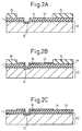
- a metallic film 14 is formed on the entire surface of the wafer 10 subjected to the ion milling, by sputtering in a vacuum atmosphere.
- the metallic film 14 is formed of two layers, i.e., an adhering metal layer (chromium (Cr) layer in this embodiment) and a copper (Cu) layer located thereon.
- the formation of the metallic film 14 of two layer structure is carried out by depositing Cr on the entire surface of the wafer 10 by sputtering to form an underlying adhering metal layer (Cr layer), and further depositing Cu thereon by sputtering to form an overlaying Cu layer having a thickness of several thousands angstroms.
- a film of photosensitive resist such as a dry film, is formed on the metallic film 14, is then exposed using a mask (not shown), and is developed to provide a patterned resist film 15.
- a patterned wiring line layer 16 of Cu having a thickness of several tens micrometers is formed by electrolytic plating using the patterned resist film 15 as a mask and the metallic film 14 as an electrical power supply layer.
- the wiring line layer 16 may be made of a material other than Cu, such as an alloy of Cu, or Al or an alloy of Al.
- the patterned wiring line layer 16 thus formed is also called "rerouting line layer”.
- the dry film i.e., the resist film 15 (Fig. 2B)
- a resist peeling solution such as an aqueous solution of sodium hydroxide (NaOH).
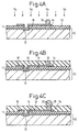
- a film of photosensitive resist such as a dry film, is formed so as to cover the metallic film 14 and the wiring line layer 16, is then exposed using a mask (not shown), and is developed to form a patterned resist film 17 having openings which expose part of the wiring line layer 16.
- via posts 18 are formed by electrolytic plating using the patterned resist film 17 as a mask and the metallic film 14 as an electrical power supply layer.
- a barrier metal layer (not shown) may be additionally formed on the top of the via post 18 also by electrolytic plating, as required.
- the via post 18 is used as a means to connect a product semiconductor device to an external electrical circuit.
- the dry film i.e., the resist film 17 (Fig. 3B)
- a resist peeling solution such as a solution of sodium hydroxide (NaOH)
- the exposed metallic film 14 is then removed by etching.
- the upper layer of Cu of the film 14 is first removed using an etchant in which Cu is dissolved, and the lower layer of Cr of the film 14 is then removed using an etchant in which Cr is dissolved.
- the polyimide layer 13 is exposed as shown in the drawing.
- the surface of the polyimide layer 13, which is now exposed, is subjected to dry etching using nitrogen (N 2 ) gas, as illustrated in the drawing.
- This dry etching restores an insulation resistance of the polyimide layer 13 which may have been more or less lowered by the former ion milling to a sufficient value.
- the dry etching using nitrogen gas may be sputter etching or chemical dry etching (reactive plasma etching).
- the wafer 10 provided with the wiring line layer 16 (rerouting line layer) accompanied by the via posts 18 is encapsulated by a resin.
- a well-known method such as those known from Japanese Unexamined Patent Publication (Kokai) No. 10-79362 (JP-A-10-79362), as follows.
- an encapsulating mold (not shown) having top and bottom members is prepared and is heated to a predetermined temperature.
- a resin film is then attached to the lower face of the top member by sucking, the wafer 10 is placed on the bottom member, and a thermoset resin having a great adhesion is placed on the wafer 10.
- the resin is then melted and extended over the entire surface of the wafer 10 by heat of the mold and pressure by pressing, so as to expose the top ends of the respective via posts 18, and is set in the mold.
- the encapsulated wafer 10 accompanied by the resin film is removed from the mold, and the resin film is then peeled from the wafer 10. In this way, the wafer 10 having the surface covered with an encapsulating resin 19 so as to expose the top ends of the via posts 18 is obtained, as shown in Fig. 4B.
- a solder ball 20 is placed on the exposed top end of the via post 18, and is reflowed to be fixed to the via post 18.
- the wafer 10 provided with the wiring line layer 16, via posts 18 with solder balls 20, and the layer of encapsulating resin 19 is cut by dicer or the like into individual semiconductor elements (i.e., semiconductor chips).
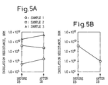
- Figs. 5A and 5B show changes in insulation resistances of polyimide layers 13 before and after being subjected to an ion beam (IB) for the ion milling illustrated in Fig. 1B.
- Fig. 5A represents the case of the use of a mixed gas of Ar + H 2 (example of the invention), and
- Fig. 5B represents the case of the use of Ar only (comparative example). All experiments were conducted under the following conditions: Ar flow rate of 9 sccm, beam voltage of 700 volts, base pressure of 8 ⁇ 10 -7 millibars, processing pressure of 6 ⁇ 10 -4 millibars, and processing time of 5 seconds. Further, in the experiments of the invention, H 2 was fed at a flow rate of 1.0 sccm in addition to Ar, the H 2 flow rate being 10% by volume of the total of Ar and H 2 flow rates.
- three samples respectively showed insulation resistances of 5.6 ⁇ 10 5 ohms, 1.6 ⁇ 10 9 ohms, and 3.8 ⁇ 10 10 ohms, before being subjected to the ion beam (which is indicated in the drawings as "Before IB"), and 1.5 ⁇ 10 7 ohms, 7.6 ⁇ 10 8 ohms, and 2.5 ⁇ 10 11 ohms, after being subjected to the ion beam (which is indicated in the drawings as "After IB").
- a sample showed an insulation resistances of 1.8 ⁇ 10 9 ohms and 8.3 ⁇ 10 5 ohms before and after being subjected to the ion beam, respectively.
- Figs. 6A and 6B show profiles of elements in the direction of depth of a semiconductor chip measured using a combination of sputter etching by Ar gas with Auger electron spectroscopy.
- Fig. 6A shows results obtained using a sample having electrodes or pads 12 before being subjected to the ion milling illustrated in Fig. 1B, which had a surface at which a naturally oxidized film F (Fig. 1A) was formed.
- changes in compositions of elements in this case, aluminum (Al) and oxygen (O) present in the vertical plane including the Al layer 12 are shown against processing time (time for sputter etching).
- Fig. 7 shows the relation between a processing time for the ion milling (time for directing an ion beam to the polyimide layer 13) and a resistance between two points in the wiring line layer 12.
- the resistance between two points in the wiring line layer means the total electrical resistance between an arbitrary set of two electrodes in the wiring line layer 12, including a resistance of a wiring line interconnecting the electrodes.
- the results reveal that an increased content of H 2 in an ion milling gas increased a processing time for the removal of a naturally oxidized Al layer at the surface of a wiring line layer, although it was expected that the more the H 2 concentration, the larger its reducing effect, and the oxidized Al layer can be removed in a shorter time.
- an increased content of H 2 increases a total pressure of a mixed gas of Ar + H 2 , and lessens the energy of bombarding Ar ions. Consequently, in the invention, the ion milling gas preferably contains 5 to 33% by volume of H 2 and 95 to 67% by volume of Ar. More preferably, the ion milling gas contains 5 to 10% by volume of H 2 and 95 to 90% by volume of Ar.
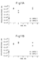
- Figs. 11A and 11B demonstrate restoration of insulation resistances of polyimide layers 13 by sputter etching using N 2 gas in the step illustrated in Fig. 4A.
- Fig. 11A represents the case of the use of 90% Ar + 10% H 2 for the ion milling in the step illustrated in Fig. 1B (example of the invention), and
- Fig. 11B represents the case of the use of Ar only (comparative example).
- the ion milling was carried out at the same conditions as those used before except that the processing time was 300 seconds (5 minutes) herein.
- Example of the Invention Insulation Resistances, ohms Processing Time, min.
- Sample I Sample II 0 3.0 ⁇ 10 5 3.7 ⁇ 10 5 1 2.3 ⁇ 10 12 1.9 ⁇ 10 12 2 1.2 ⁇ 10 11 9.3 ⁇ 10 9 5 1.3 ⁇ 10 12 2.0 ⁇ 10 13 Comparative Example Insulation Resistances, ohms Processing Time, min.
- Sample I Sample II 0 3.7 ⁇ 10 4 4.2 ⁇ 10 4 1 7.0 ⁇ 10 10 2.8 ⁇ 10 10 2 1.6 ⁇ 10 11 3.9 ⁇ 10 11 5 8.3 ⁇ 10 10 4.0 ⁇ 10 9
- the use of a mixed gas of Ar + H 2 for the ion milling enables an insulation resistance of the polyimide layer 13 to be less reduced, or even to be enhanced, as shown in Fig. 5A.
- sputter etching by N 2 gas is conducted at the stage of the polyimide layer 13 being re-exposed after the formation of rerouting line layer 16, as illustrated in Fig. 4A, which can restore an insulation resistance of the polyimide layer 13 to a sufficient value.
- a sample having an insulation film having a restored insulation resistance of 5.60 ⁇ 10 12 was subjected to a reflow cycle test in which the sample was heated from room temperature to 240°C at a rate of 0.25°C/min and was then cooled to room temperature. After a predetermined cycle, an insulation resistance of the insulation film was measured. Results are shown in the table below and Fig. 13. Reflow Cycle Test Number of Reflow Cycles Insulation Resistances, ohms 0 5.60 ⁇ 10 12 5 4.20 ⁇ 10 11 10 4.00 ⁇ 10 12
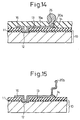
- the semiconductor device has a CSP structure in which the via posts 18 for external connection are provided on the rerouting line layer 16, the invention can be, of course, applied to a semiconductor device which does not have such via posts.
- a treatment for restoring an insulation resistance of the polyimide layer 13 i.e., sputter etching by N 2 gas is conducted at a step following the step formerly illustrated in Fig. 2C (a step after the removal of the exposed metallic film 14).
- solder resist layer may be formed by either applying a solder resist material to the surface of the wafer 10 provided with the rerouting line layer 16 by screen printing so as to open via holes for the connection between the rerouting line layer 16 and the solder ball 20a through the formed via hole, or applying a photosensitive solder resist material, and then exposing and developing the resultant layer of resist material to be patterned.
- the semiconductor device uses solder balls for external connection terminals, others may be, of course, used for external connection terminals.
- a wire may be used for an external connection terminal.
- FIG. 15 An example of a semiconductor device using wires for external connection terminal is shown in Fig. 15 and can be produced as follows, for instance.
- wires 20b of gold (Au) for external connection terminal are bonded to the rerouting line layer 16 through the openings in the resist film 17 by wire bonding technique.
- the resist film 17 is removed, the surface of the wire 20b is plated with an alloy of nickel and cobalt (Ni-Co) using the metallic film 14 as an electrical power supply layer, and the metallic film 14 exposed on the surface of the wafer 10 is then removed.
- Ni-Co nickel and cobalt
- treatment for restoring an insulation resistance of the polyimide layer 13 i.e., dry etching by N 2 gas is conducted at a step after the removal of the exposed metallic film 14.
- the invention makes it possible to provide a semiconductor device comprising an insulation film covering a semiconductor chip so as to expose electrodes or pads fabricated in the chip and wiring lines located on the insulation film, the insulation film having sufficient insulation properties, and the electrode of the chip being satisfactorily connected to the wiring line on the insulation film.
Landscapes
- Internal Circuitry In Semiconductor Integrated Circuit Devices (AREA)
Applications Claiming Priority (2)
| Application Number | Priority Date | Filing Date | Title |
|---|---|---|---|
| JP12712099 | 1999-05-07 | ||
| JP12712099 | 1999-05-07 |
Publications (3)
| Publication Number | Publication Date |
|---|---|
| EP1050905A2 true EP1050905A2 (fr) | 2000-11-08 |
| EP1050905A3 EP1050905A3 (fr) | 2001-09-12 |
| EP1050905B1 EP1050905B1 (fr) | 2017-06-21 |
Family
ID=14952111
Family Applications (1)
| Application Number | Title | Priority Date | Filing Date |
|---|---|---|---|
| EP00303721.5A Expired - Lifetime EP1050905B1 (fr) | 1999-05-07 | 2000-05-03 | Procédé de fabrication d'un dispositif semiconducteur avec couche isolante |
Country Status (4)
| Country | Link |
|---|---|
| US (1) | US6200888B1 (fr) |
| EP (1) | EP1050905B1 (fr) |
| KR (1) | KR100700392B1 (fr) |
| TW (1) | TW465057B (fr) |
Cited By (2)
| Publication number | Priority date | Publication date | Assignee | Title |
|---|---|---|---|---|
| EP1321982A3 (fr) * | 2001-12-21 | 2009-07-29 | Texas Instruments Incorporated | Procédé de brasage direct sur des plages de cuivre dans des circuits intégrés au niveau de plaquettes |
| EP2849209A1 (fr) * | 2013-09-16 | 2015-03-18 | SPTS Technologies Limited | Prénettoyage de structure semi-conductrice |
Families Citing this family (24)
| Publication number | Priority date | Publication date | Assignee | Title |
|---|---|---|---|---|
| US6965165B2 (en) * | 1998-12-21 | 2005-11-15 | Mou-Shiung Lin | Top layers of metal for high performance IC's |
| US7230340B2 (en) * | 2000-10-18 | 2007-06-12 | Megica Corporation | Post passivation interconnection schemes on top of the IC chips |
| US6495442B1 (en) | 2000-10-18 | 2002-12-17 | Magic Corporation | Post passivation interconnection schemes on top of the IC chips |
| US6268274B1 (en) * | 1999-10-14 | 2001-07-31 | Taiwan Semiconductor Manufacturing Company | Low temperature process for forming inter-metal gap-filling insulating layers in silicon wafer integrated circuitry |
| US6653240B2 (en) * | 2001-01-12 | 2003-11-25 | International Business Machines Corporation | FIB/RIE method for in-line circuit modification of microelectronic chips containing organic dielectric |
| JP3888854B2 (ja) * | 2001-02-16 | 2007-03-07 | シャープ株式会社 | 半導体集積回路の製造方法 |
| JP4790157B2 (ja) * | 2001-06-07 | 2011-10-12 | ルネサスエレクトロニクス株式会社 | 半導体装置 |
| US6869831B2 (en) * | 2001-09-14 | 2005-03-22 | Texas Instruments Incorporated | Adhesion by plasma conditioning of semiconductor chip surfaces |
| JP3580803B2 (ja) * | 2002-08-09 | 2004-10-27 | 沖電気工業株式会社 | 半導体装置 |
| JP2004103911A (ja) * | 2002-09-11 | 2004-04-02 | Shinko Electric Ind Co Ltd | 配線形成方法 |
| KR100461002B1 (ko) * | 2002-10-17 | 2004-12-09 | 삼성전자주식회사 | 언더컷 메탈 배선방법 |
| JP4360873B2 (ja) * | 2003-09-18 | 2009-11-11 | ミナミ株式会社 | ウエハレベルcspの製造方法 |
| US7459790B2 (en) | 2003-10-15 | 2008-12-02 | Megica Corporation | Post passivation interconnection schemes on top of the IC chips |
| JP4376715B2 (ja) * | 2004-07-16 | 2009-12-02 | 三洋電機株式会社 | 半導体装置の製造方法 |
| US7714414B2 (en) * | 2004-11-29 | 2010-05-11 | Taiwan Semiconductor Manufacturing Co., Ltd. | Method and apparatus for polymer dielectric surface recovery by ion implantation |
| JP2006303379A (ja) * | 2005-04-25 | 2006-11-02 | Seiko Epson Corp | 半導体装置の製造方法 |
| US7468545B2 (en) * | 2005-05-06 | 2008-12-23 | Megica Corporation | Post passivation structure for a semiconductor device and packaging process for same |
| JP4061506B2 (ja) * | 2005-06-21 | 2008-03-19 | セイコーエプソン株式会社 | 半導体装置の製造方法 |
| US7582556B2 (en) | 2005-06-24 | 2009-09-01 | Megica Corporation | Circuitry component and method for forming the same |
| DE102006028811A1 (de) * | 2006-06-21 | 2007-12-27 | Qimonda Ag | Verfahren zum Aufbringen von Lot auf Umverdrahtungsleitungen |
| US8174131B2 (en) * | 2009-05-27 | 2012-05-08 | Globalfoundries Inc. | Semiconductor device having a filled trench structure and methods for fabricating the same |
| US20120315710A1 (en) * | 2010-03-04 | 2012-12-13 | Kazuyuki Hozawa | Method for producing reconstituted wafers and method for producing semiconductor devices |
| US8957694B2 (en) | 2012-05-22 | 2015-02-17 | Broadcom Corporation | Wafer level package resistance monitor scheme |
| US9704769B2 (en) | 2014-02-27 | 2017-07-11 | STATS ChipPAC Pte. Ltd. | Semiconductor device and method of forming encapsulated wafer level chip scale package (EWLCSP) |
Citations (1)
| Publication number | Priority date | Publication date | Assignee | Title |
|---|---|---|---|---|
| US4357203A (en) | 1981-12-30 | 1982-11-02 | Rca Corporation | Plasma etching of polyimide |
Family Cites Families (7)
| Publication number | Priority date | Publication date | Assignee | Title |
|---|---|---|---|---|
| US4278493A (en) * | 1980-04-28 | 1981-07-14 | International Business Machines Corporation | Method for cleaning surfaces by ion milling |
| JPS6187338A (ja) * | 1984-10-05 | 1986-05-02 | Nec Corp | 多重ビ−ム照射Si表面ドライ洗浄法 |
| JP2639052B2 (ja) * | 1989-02-07 | 1997-08-06 | 富士通株式会社 | 半導体装置の製造方法 |
| JPH02246246A (ja) * | 1989-03-20 | 1990-10-02 | Fujitsu Ltd | 半導体装置の製造方法 |
| JP3469251B2 (ja) * | 1990-02-14 | 2003-11-25 | 株式会社東芝 | 半導体装置の製造方法 |
| JPH0922896A (ja) * | 1995-07-07 | 1997-01-21 | Toshiba Corp | 金属膜の選択的形成方法 |
| JPH1167702A (ja) * | 1997-08-25 | 1999-03-09 | Mitsubishi Electric Corp | 半導体電極の清浄方法及び清浄装置 |
-
2000
- 2000-05-03 EP EP00303721.5A patent/EP1050905B1/fr not_active Expired - Lifetime
- 2000-05-04 US US09/564,682 patent/US6200888B1/en not_active Expired - Lifetime
- 2000-05-04 KR KR1020000023971A patent/KR100700392B1/ko not_active Expired - Lifetime
- 2000-05-06 TW TW089108694A patent/TW465057B/zh not_active IP Right Cessation
Patent Citations (1)
| Publication number | Priority date | Publication date | Assignee | Title |
|---|---|---|---|---|
| US4357203A (en) | 1981-12-30 | 1982-11-02 | Rca Corporation | Plasma etching of polyimide |
Cited By (4)
| Publication number | Priority date | Publication date | Assignee | Title |
|---|---|---|---|---|
| EP1321982A3 (fr) * | 2001-12-21 | 2009-07-29 | Texas Instruments Incorporated | Procédé de brasage direct sur des plages de cuivre dans des circuits intégrés au niveau de plaquettes |
| EP2849209A1 (fr) * | 2013-09-16 | 2015-03-18 | SPTS Technologies Limited | Prénettoyage de structure semi-conductrice |
| CN104576316A (zh) * | 2013-09-16 | 2015-04-29 | Spts技术有限公司 | 预清洗半导体结构 |
| US10978291B2 (en) | 2013-09-16 | 2021-04-13 | Spts Technologies Limited | Pre-cleaning a semiconductor structure |
Also Published As
| Publication number | Publication date |
|---|---|
| KR100700392B1 (ko) | 2007-03-28 |
| EP1050905A3 (fr) | 2001-09-12 |
| KR20000077164A (ko) | 2000-12-26 |
| US6200888B1 (en) | 2001-03-13 |
| TW465057B (en) | 2001-11-21 |
| EP1050905B1 (fr) | 2017-06-21 |
Similar Documents
| Publication | Publication Date | Title |
|---|---|---|
| US6200888B1 (en) | Method of producing semiconductor device comprising insulation layer having improved resistance and semiconductor device produced thereby | |
| US6362087B1 (en) | Method for fabricating a microelectronic fabrication having formed therein a redistribution structure | |
| KR100658543B1 (ko) | 반도체 장치 및 그 제조 방법 | |
| US3663184A (en) | Solder bump metallization system using a titanium-nickel barrier layer | |
| US5244833A (en) | Method for manufacturing an integrated circuit chip bump electrode using a polymer layer and a photoresist layer | |
| USRE46147E1 (en) | Semiconductor device and method of fabricating the same | |
| EP0261799B1 (fr) | Procédé de fabrication d'une électrode de connexion d'un dispositif semi-conducteur | |
| US7094701B2 (en) | Manufacturing method of semiconductor device | |
| KR100213152B1 (ko) | 솔더 터미널 및 그 제조방법 | |
| US5010389A (en) | Integrated circuit substrate with contacts thereon for a packaging structure | |
| CN100440460C (zh) | 半导体器件及其制造方法 | |
| US20030080428A1 (en) | Semiconductor device | |
| JP2000510288A (ja) | 集積回路及びその製造方法 | |
| KR20050087840A (ko) | 구리 상호 접속 구조체로의 본딩 구조체 및 방법 | |
| WO2004093185A2 (fr) | Appareil et procedes d'interconnexion | |
| US6278185B1 (en) | Semi-additive process (SAP) architecture for organic leadless grid array packages | |
| US12237219B2 (en) | Contact with bronze material to mitigate undercut | |
| JP3544340B2 (ja) | 半導体装置の製造方法 | |
| JP4297652B2 (ja) | 半導体装置の製造方法 | |
| JP3362573B2 (ja) | バリアメタルの形成方法 | |
| US8735277B2 (en) | Methods for producing an ultrathin semiconductor circuit | |
| US6995082B2 (en) | Bonding pad of a semiconductor device and formation method thereof | |
| JPH04217323A (ja) | 半導体装置用バンプ電極の製造方法 | |
| TWI904718B (zh) | 用於在兩個基底之間形成導電結構的方法 | |
| US20240332033A1 (en) | Method of manufacturing semiconductor devices, corresponding semiconductor device and mounting assembly |
Legal Events
| Date | Code | Title | Description |
|---|---|---|---|
| PUAI | Public reference made under article 153(3) epc to a published international application that has entered the european phase |
Free format text: ORIGINAL CODE: 0009012 |
|
| AK | Designated contracting states |
Kind code of ref document: A2 Designated state(s): AT BE CH CY DE DK ES FI FR GB GR IE IT LI LU MC NL PT SE Kind code of ref document: A2 Designated state(s): DE FR |
|
| AX | Request for extension of the european patent |
Free format text: AL;LT;LV;MK;RO;SI |
|
| PUAL | Search report despatched |
Free format text: ORIGINAL CODE: 0009013 |
|
| AK | Designated contracting states |
Kind code of ref document: A3 Designated state(s): AT BE CH CY DE DK ES FI FR GB GR IE IT LI LU MC NL PT SE |
|
| AX | Request for extension of the european patent |
Free format text: AL;LT;LV;MK;RO;SI |
|
| RIC1 | Information provided on ipc code assigned before grant |
Free format text: 7H 01L 21/768 A, 7H 01L 21/60 B |
|
| 17P | Request for examination filed |
Effective date: 20020215 |
|
| AKX | Designation fees paid |
Free format text: DE FR |
|
| 17Q | First examination report despatched |
Effective date: 20070118 |
|
| REG | Reference to a national code |
Ref country code: DE Ref legal event code: R079 Ref document number: 60049647 Country of ref document: DE Free format text: PREVIOUS MAIN CLASS: H01L0021768000 Ipc: H01L0023310000 |
|
| GRAP | Despatch of communication of intention to grant a patent |
Free format text: ORIGINAL CODE: EPIDOSNIGR1 |
|
| RIC1 | Information provided on ipc code assigned before grant |
Ipc: H01L 21/768 20060101ALI20161117BHEP Ipc: H01L 21/60 20060101ALI20161117BHEP Ipc: H01L 23/31 20060101AFI20161117BHEP |
|
| INTG | Intention to grant announced |
Effective date: 20161208 |
|
| RIN1 | Information on inventor provided before grant (corrected) |
Inventor name: KITAHARA, YUICHI, SHINKO ELECTRIC INDUSTRIE CO., L Inventor name: ITO, DAISUKE, SHINKO ELECTRIC INDUSTRIE CO., LTD. |
|
| GRAS | Grant fee paid |
Free format text: ORIGINAL CODE: EPIDOSNIGR3 |
|
| RIN1 | Information on inventor provided before grant (corrected) |
Inventor name: KITAHARA, YUICHI, SHINKO ELECTRIC INDUSTRIES CO., Inventor name: ITO, DAISUKE, SHINKO ELECTRIC INDUSTRIES CO., LTD. |
|
| GRAA | (expected) grant |
Free format text: ORIGINAL CODE: 0009210 |
|
| RAP1 | Party data changed (applicant data changed or rights of an application transferred) |
Owner name: SHINKO ELECTRIC INDUSTRIES CO. LTD. |
|
| AK | Designated contracting states |
Kind code of ref document: B1 Designated state(s): DE FR |
|
| REG | Reference to a national code |
Ref country code: DE Ref legal event code: R096 Ref document number: 60049647 Country of ref document: DE |
|
| REG | Reference to a national code |
Ref country code: DE Ref legal event code: R097 Ref document number: 60049647 Country of ref document: DE |
|
| PLBE | No opposition filed within time limit |
Free format text: ORIGINAL CODE: 0009261 |
|
| STAA | Information on the status of an ep patent application or granted ep patent |
Free format text: STATUS: NO OPPOSITION FILED WITHIN TIME LIMIT |
|
| 26N | No opposition filed |
Effective date: 20180322 |
|
| PG25 | Lapsed in a contracting state [announced via postgrant information from national office to epo] |
Ref country code: FR Free format text: LAPSE BECAUSE OF NON-PAYMENT OF DUE FEES Effective date: 20180531 |
|
| PGFP | Annual fee paid to national office [announced via postgrant information from national office to epo] |
Ref country code: DE Payment date: 20190423 Year of fee payment: 20 |
|
| REG | Reference to a national code |
Ref country code: DE Ref legal event code: R071 Ref document number: 60049647 Country of ref document: DE |