EP1051693B1 - Carte a memoire asynchrone - Google Patents
Carte a memoire asynchrone Download PDFInfo
- Publication number
- EP1051693B1 EP1051693B1 EP99900924A EP99900924A EP1051693B1 EP 1051693 B1 EP1051693 B1 EP 1051693B1 EP 99900924 A EP99900924 A EP 99900924A EP 99900924 A EP99900924 A EP 99900924A EP 1051693 B1 EP1051693 B1 EP 1051693B1
- Authority
- EP
- European Patent Office
- Prior art keywords
- circuit
- code
- terminal
- memory
- memory card
- Prior art date
- Legal status (The legal status is an assumption and is not a legal conclusion. Google has not performed a legal analysis and makes no representation as to the accuracy of the status listed.)
- Expired - Lifetime
Links
Images
Classifications
-
- G—PHYSICS
- G07—CHECKING-DEVICES
- G07F—COIN-FREED OR LIKE APPARATUS
- G07F7/00—Mechanisms actuated by objects other than coins to free or to actuate vending, hiring, coin or paper currency dispensing or refunding apparatus
- G07F7/08—Mechanisms actuated by objects other than coins to free or to actuate vending, hiring, coin or paper currency dispensing or refunding apparatus by coded identity card or credit card or other personal identification means
- G07F7/10—Mechanisms actuated by objects other than coins to free or to actuate vending, hiring, coin or paper currency dispensing or refunding apparatus by coded identity card or credit card or other personal identification means together with a coded signal, e.g. in the form of personal identification information, like personal identification number [PIN] or biometric data
- G07F7/1008—Active credit-cards provided with means to personalise their use, e.g. with PIN-introduction/comparison system
-
- G—PHYSICS
- G06—COMPUTING OR CALCULATING; COUNTING
- G06F—ELECTRIC DIGITAL DATA PROCESSING
- G06F3/00—Input arrangements for transferring data to be processed into a form capable of being handled by the computer; Output arrangements for transferring data from processing unit to output unit, e.g. interface arrangements
- G06F3/06—Digital input from, or digital output to, record carriers, e.g. RAID, emulated record carriers or networked record carriers
- G06F3/08—Digital input from, or digital output to, record carriers, e.g. RAID, emulated record carriers or networked record carriers from or to individual record carriers, e.g. punched card, memory card, integrated circuit [IC] card or smart card
-
- G—PHYSICS
- G06—COMPUTING OR CALCULATING; COUNTING
- G06K—GRAPHICAL DATA READING; PRESENTATION OF DATA; RECORD CARRIERS; HANDLING RECORD CARRIERS
- G06K7/00—Methods or arrangements for sensing record carriers, e.g. for reading patterns
- G06K7/0008—General problems related to the reading of electronic memory record carriers, independent of its reading method, e.g. power transfer
-
- G—PHYSICS
- G06—COMPUTING OR CALCULATING; COUNTING
- G06Q—INFORMATION AND COMMUNICATION TECHNOLOGY [ICT] SPECIALLY ADAPTED FOR ADMINISTRATIVE, COMMERCIAL, FINANCIAL, MANAGERIAL OR SUPERVISORY PURPOSES; SYSTEMS OR METHODS SPECIALLY ADAPTED FOR ADMINISTRATIVE, COMMERCIAL, FINANCIAL, MANAGERIAL OR SUPERVISORY PURPOSES, NOT OTHERWISE PROVIDED FOR
- G06Q20/00—Payment architectures, schemes or protocols
- G06Q20/30—Payment architectures, schemes or protocols characterised by the use of specific devices or networks
- G06Q20/34—Payment architectures, schemes or protocols characterised by the use of specific devices or networks using cards, e.g. integrated circuit [IC] cards or magnetic cards
- G06Q20/341—Active cards, i.e. cards including their own processing means, e.g. including an IC or chip
-
- G—PHYSICS
- G07—CHECKING-DEVICES
- G07F—COIN-FREED OR LIKE APPARATUS
- G07F7/00—Mechanisms actuated by objects other than coins to free or to actuate vending, hiring, coin or paper currency dispensing or refunding apparatus
- G07F7/08—Mechanisms actuated by objects other than coins to free or to actuate vending, hiring, coin or paper currency dispensing or refunding apparatus by coded identity card or credit card or other personal identification means
- G07F7/0806—Details of the card
- G07F7/0833—Card having specific functional components
- G07F7/084—Additional components relating to data transfer and storing, e.g. error detection, self-diagnosis
-
- G—PHYSICS
- G11—INFORMATION STORAGE
- G11C—STATIC STORES
- G11C7/00—Arrangements for writing information into, or reading information out from, a digital store
- G11C7/10—Input/output [I/O] data interface arrangements, e.g. I/O data control circuits, I/O data buffers
- G11C7/1051—Data output circuits, e.g. read-out amplifiers, data output buffers, data output registers, data output level conversion circuits
- G11C7/1063—Control signal output circuits, e.g. status or busy flags, feedback command signals
-
- G—PHYSICS
- G11—INFORMATION STORAGE
- G11C—STATIC STORES
- G11C7/00—Arrangements for writing information into, or reading information out from, a digital store
- G11C7/10—Input/output [I/O] data interface arrangements, e.g. I/O data control circuits, I/O data buffers
- G11C7/1078—Data input circuits, e.g. write amplifiers, data input buffers, data input registers, data input level conversion circuits
- G11C7/109—Control signal input circuits
-
- G—PHYSICS
- G11—INFORMATION STORAGE
- G11C—STATIC STORES
- G11C8/00—Arrangements for selecting an address in a digital store
- G11C8/06—Address interface arrangements, e.g. address buffers
Definitions
- the invention relates to memory cards, i.e. cards which essentially contain a memory and its addressing circuits for recording and reading data or information.
- the memory of these cards is saved and / or read using a terminal, such as a card reader, that communicates with memory by electrical signals applied by through contacts.
- the electrical signals are developed by the terminal according to normative protocols individuals who have the particularity of being of the type synchronous with indirect addressing.
- the document FR2635598 describes a card whose memory is saved and / or read using a terminal, such as a card reader, which communicates with memory by electrical signals applied through of contacts to an addressing circuit.
- the circuit card integrated includes a control element, for example a central processing unit (CPU), data memory, a program memory and a contact part intended for ensuring electrical contact with the recorder from the menu.
- CPU central processing unit
- An object of the present invention is therefore to achieve a memory card that does not have the aforementioned drawbacks.
- the card according to the invention has the advantage for some minor additional amenities, in addition of the above wired functions, to be totally compatible with readers of the existing fleet.
- it is particularly advantageous to ability to use card readers microprocessor, which is currently impossible with current memory cards.
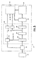
- the memory card comprises, in addition to the elements indicated above, a device 20 which makes the connection between, on the one hand the plurality of contacts 16 and, on the other hand, the addressing circuit 12 and the control circuit 14.
- the link between terminal 18 and card 40 is effected by the plurality of contacts 16 in applying electrical signals to these contacts which are standardized according to so-called communication protocols asynchronous.
- These protocols can be of different known types and especially those known as the designation RS232 with regard to a link commonly used series between a computer says personnel and its peripherals or the V22 designations, V23, etc ... with regard to the modem connection.
- the chosen protocol is implemented by the terminal and must be understood by the memory card at the level of the reception and analysis circuit 22.
- This last circuit 22 receives the signals received from the terminal and analyzes it to check its integrity.
- the terminal is designed to add a redundant information in the transmitted signals, information that the reception and analysis circuit 22 is able to verify its presence and value. he can be the presence of a parity bit or a Redundant cyclic code. It should be noted that many communication protocols provide for such redundancy to verify the integrity of the information transmitted.
- the circuit reception and analysis 22 is provided to provide the terminal an acknowledgment of receipt such as a code indicating that the card has received the information and that its integrity is correct. Otherwise, it provides an error code.
- acknowledgments are provided in some communication protocols.
- addressing the memory 10 is done directly by an address code which is received and analyzed by the receiving circuit and analysis 22.
- Such direct addressing can be achieved by setting implements a protocol known by the abbreviation I2C, protocol used for device control computers.
- This address code is detected by the circuit of interpretation and referral 24 which transmits it to the address register 26.
- the interpretation and referral circuit 24 detects also the data and instruction codes and the transmits to one or more registers 28, the codes contained in register 28 being made available to the control circuit 14.
- control 14 When the instruction has been carried out, the control 14 is provided to generate a status code indicating the execution of the instruction or of a code error indicating that the instruction was not executed. This code is transmitted to terminal 18 by through the output register 32 receiving the control circuit 14 and circuit code transmission 34.
- the code read in memory is transmitted to the terminal by through output register 32 and the circuit 34.
- the output register 32 can be under the form of two registers, one for status codes and the other for the data read from memory 10.
Landscapes
- Engineering & Computer Science (AREA)
- General Physics & Mathematics (AREA)
- Physics & Mathematics (AREA)
- Theoretical Computer Science (AREA)
- Microelectronics & Electronic Packaging (AREA)
- Business, Economics & Management (AREA)
- Strategic Management (AREA)
- Artificial Intelligence (AREA)
- Computer Vision & Pattern Recognition (AREA)
- Computer Networks & Wireless Communication (AREA)
- Accounting & Taxation (AREA)
- General Business, Economics & Management (AREA)
- General Engineering & Computer Science (AREA)
- Human Computer Interaction (AREA)
- Credit Cards Or The Like (AREA)
- Storage Device Security (AREA)
- Communication Control (AREA)
- Techniques For Improving Reliability Of Storages (AREA)
Description
- une remise à zéro de la carte, notamment du compteur d'adresse de la mémoire, soit à la mise sous tension, soit par un signal de remise à zéro sur une broche prévue à cet effet ;
- un positionnement du compteur d'adresse de la mémoire à la bonne adresse par l'application d'un nombre d'impulsions déterminé sur une broche correspondant aux impulsions d'horloge ;
- une commande d'enregistrement ou de lecture dans la mémoire par une combinaison de signaux appliqués sur une broche Entrée/Sortie et sur une autre broche qui peut être la broche remise à zéro, la broche horloge ou toute autre broche.
- La répétition des messages augmente le temps nécessaire à une transaction.
- En outre, il est possible d'avoir des transactions erronées suite à ces bruits électriques.
- L'adressage de la mémoire est effectué par l'intermédiaire d'un compteur d'impulsions qui compte la série des impulsions qui lui sont appliquées et le code affiché par le compteur à la fin de cette série constitue le code d'adresse de la mémoire. Cet adressage, dit indirect, implique une certaine durée due au comptage des impulsions et constitue une source d'erreur, par exemple si une impulsion n'est pas prise en compte pour diverses raisons.
- Aucun contrôle de l'intégrité de la donnée ou de la commande reçue n'est effectué, d'où une absence de sécurité.
- Le protocole de transaction est du type synchrone, ce qui implique un synchronisme rigoureux entre le terminal et la carte à mémoire, synchronisme qu'il est parfois difficile d'obtenir et de maintenir au cours de la transaction par suite de perturbations extérieures.
- Aucun accusé de réception n'est effectué lors de réception de la donnée ou de la commande reçue.
- Aucune vérification de la bonne exécution de la commande n'est effectuée.
- la communication entre le terminal et la carte à mémoire soit effectuée selon un protocole de communication asynchrone ;
- l'adressage de la mémoire soit effectué par adressage direct ;
- l'information qui est reçue par la carte et relative à une adresse, une commande ou une donnée soit vérifiée ;
- la carte à mémoire effectue un accusé de réception au terminal de l'information reçue et de son intégrité ;
- la carte à mémoire transmette au terminal une information de bonne exécution de la commande.
- un circuit de réception et d'analyse des signaux électriques appliqués aux contacts de la carte à mémoire par le terminal, ledit circuit de réception et d'analyse fournissant des messages et des codes ;
- un circuit d'interprétation et d'aiguillage des codes fournis par le circuit d'analyse selon qu'il s'agit d'un code d'adresse de la mémoire, d'un code de donnée ou d'un code de commande ;
- un registre d'adresse qui enregistre le code d'adresse fourni par le circuit d'interprétation et d'aiguillage pour le mettre à disposition du circuit d'adressage ;
- au moins un registre de données qui enregistre le code de commande de l'opération à réaliser sur la mémoire ou le code de la donnée à y enregistrer éventuellement pour mettre lesdits codes à la disposition du circuit de contrôle en vue d'en effectuer l'opération indiquée par le code de commande,
- au moins un registre de sortie qui enregistre le code lu dans la mémoire ou le code d'état d'exécution de la commande, fourni par le circuit de contrôle, et
- un circuit de transmission aux contacts des codes fournis par le registre de sortie et des messages fournis par le circuit de réception et d'analyse pour les transmettre au terminal.
- une mémoire 10 du type permettant la lecture et l'enregistrement de données sous forme de chiffres binaires dans des cellules élémentaires,
- un circuit d'adressage 12 de la mémoire 10 pour sélectionner un ou des groupes de cellules élémentaires correspondant chacun à une donnée à lire ou à enregistrer,
- un circuit de contrôle 14 de la mémoire 10 et du circuit d'adressage 12 pour enregistrer ou lire les cellules de la mémoire 10 à une adresse indiquée au circuit d'adressage 12, et
- une pluralité de contacts 16 disposés sur l'un des côtés de la carte pour réaliser les liaisons électriques entre un terminal 18 et la carte à mémoire.
- un circuit de réception et d'analyse 22 des signaux électriques reçus sur les contacts 16 pour analyser les signaux électriques et fournir d'une part des messages au terminal 18 et, d'autre part, des codes représentatifs de données, d'adresses de cellules de la mémoire et de commandes ou instructions à effectuer,
- un circuit d'interprétation et d'aiguillage 24 des codes fournis par le circuit de réception et d'analyse 22,
- un registre d'adresse 26 pour enregistrer le code d'adresse transmis par le terminal et le mettre à la disposition du circuit d'adressage 12,
- au moins un registre de données 28 pour enregistrer le code de donnée ou le code d'instruction transmis par le terminal et le mettre à la disposition du circuit de contrôle 14,
- au moins un registre de sortie 32 pour enregistrer le code lu dans la mémoire 10 ou l'état d'exécution de l'instruction, et
- un circuit de transmission 34 du code contenu dans le registre de sortie 32 vers le terminal 18 par l'intermédiaire des contacts 16.
- le terminal génère une instruction selon un programme d'application adapté à la carte à mémoire selon l'invention, cette instruction comportant au moins un code d'instruction, un code d'adresse et un code de donnée, l'ensemble constituant un message,
- le terminal élabore une information de redondance telle qu'un chiffre de parité ou un code cyclique redondant et l'introduit dans le message constitué des codes à transmettre,
- le terminal transmet ces codes à la carte à mémoire en mode asynchrone par l'intermédiaire des contacts 16,
- le circuit de réception et d'analyse 22 valide le message reçu par la carte à mémoire,
- le circuit de réception et d'analyse 22 transmet un accusé de réception du message au terminal par l'intermédiaire du circuit de transmission en indiquant par un code la bonne ou la mauvaise réception du message,
- le circuit de contrôle 14 exécute l'instruction, et
- le circuit de contrôle 14 transmet au terminal un message attestant l'exécution ou non de l'instruction par l'intermédiaire du registre de sortie 32 et: du circuit de transmission 34.
Claims (7)
- Carte à mémoire (40) à contacts (16) comprenant une mémoire (10) apte à coopérer avec un terminal (18) par l'intermédiaire de circuits d'accès comprenant un circuit d'adressage (12) et un circuit de contrôle (14), caractérisée en ce que les circuits d'accès à la mémoire (10) comprennent en outre :un circuit de réception et d'analyse (22) des signaux électriques appliqués aux contacts (16) de la carte à mémoire (40) par le terminal (18), ledit circuit de réception et d'analyse fournissant des messages et des codes ;un circuit d'interprétation et d'aiguillage (24) des codes fournis par le circuit de réception et d'analyse (22) selon qu'il s'agit d'un code d'adresse de la mémoire, d'un code de donnée ou d'un code de commande ou d'instruction ;un registre d'adresse (26) qui enregistre le code d'adresse fourni par le circuit d'interprétation et d'aiguillage pour le mettre à disposition du circuit d'adressage (12) ;au moins un registre de données qui enregistre le code de commande de l'opération à réaliser sur la mémoire ou le code de la donnée à y enregistrer éventuellement pour mettre lesdits codes à la disposition du circuit de contrôle (14) en vue d'en effectuer l'opération indiquée par le code de commande ;au moins un registre de sortie (32) qui enregistre le code lu dans la mémoire (10) ou le code d'état d'exécution de la commande, fourni par le circuit de contrôle (14), etun circuit de transmission (34) aux contacts des codes fournis par le registre de sortie (32) et des messages fournis par le circuit de réception et d'analyse pour les transmettre au terminal (18).
- Carte à mémoire selon la revendication 1, caractérisée en ce le circuit de réception et d'analyse (22) est apte à échanger des données selon un protocole de communication asynchrone.
- Carte à mémoire selon la revendication 1, caractérisée en ce que le circuit de réception et d'analyse (22) est apte à échanger des données avec contrôle d'intégrité du message correspondant aux signaux électriques transmis.
- Carte à mémoire selon la revendication 1, caractérisée en ce que le circuit de réception et d'analyse (22) est apte à détecter et comprendre des signaux électriques transmis par le terminal (18) selon un protocole de communication asynchrone avec contrôle d'intégrité du message correspondant aux signaux électriques transmis.
- Carte à mémoire selon l'une des revendications précédentes, caractérisée en ce que le circuit: de transmission (34) est apte à transmettre les messages fournis par le circuit de réception et d'analyse (22) et les codes fournis par le registre de sortie (32) sous une forme détectable et compréhensible par le terminal (18) selon le protocole de communication asynchrone.
- Carte à mémoire selon l'une des revendications précédentes, caractérisée en ce que le circuit de réception et d'analyse (22) est apte à générer un signal indiquant la réception correcte et complète des signaux transmis par le terminal, ledit signal étant appliqué à un circuit de transmission (34).
- Carte à mémoire selon l'une des revendications précédentes, caractérisée en ce que le circuit de contrôle est apte à générer un code d'état indiquant l'exécution ou non de l'instruction.
Applications Claiming Priority (3)
| Application Number | Priority Date | Filing Date | Title |
|---|---|---|---|
| FR9800859 | 1998-01-27 | ||
| FR9800859A FR2774196B1 (fr) | 1998-01-27 | 1998-01-27 | Carte a memoire asynchrone |
| PCT/FR1999/000062 WO1999038130A1 (fr) | 1998-01-27 | 1999-01-15 | Carte a memoire asynchrone |
Publications (2)
| Publication Number | Publication Date |
|---|---|
| EP1051693A1 EP1051693A1 (fr) | 2000-11-15 |
| EP1051693B1 true EP1051693B1 (fr) | 2003-05-28 |
Family
ID=9522216
Family Applications (1)
| Application Number | Title | Priority Date | Filing Date |
|---|---|---|---|
| EP99900924A Expired - Lifetime EP1051693B1 (fr) | 1998-01-27 | 1999-01-15 | Carte a memoire asynchrone |
Country Status (14)
| Country | Link |
|---|---|
| US (1) | US6585164B1 (fr) |
| EP (1) | EP1051693B1 (fr) |
| JP (1) | JP4167395B2 (fr) |
| KR (1) | KR20010034402A (fr) |
| CN (1) | CN1149517C (fr) |
| AR (1) | AR014504A1 (fr) |
| AU (1) | AU757905B2 (fr) |
| BR (1) | BR9907284B1 (fr) |
| CA (1) | CA2319768A1 (fr) |
| DE (1) | DE69908303T2 (fr) |
| ES (1) | ES2201659T3 (fr) |
| FR (1) | FR2774196B1 (fr) |
| WO (1) | WO1999038130A1 (fr) |
| ZA (1) | ZA99572B (fr) |
Families Citing this family (3)
| Publication number | Priority date | Publication date | Assignee | Title |
|---|---|---|---|---|
| FR2800487B1 (fr) | 1999-10-29 | 2001-11-30 | Schlumberger Systems & Service | Procede d'authentification du resultat d'une commande dans un jeton |
| DE10336121B4 (de) * | 2003-08-06 | 2006-10-26 | Infineon Technologies Ag | Serielle asynchrone Schnittstelle mit SLIP-Kodierung/Dekodierung und CRC-Prüfung im Sende- und Empfangspfad |
| CN102880842B (zh) | 2012-08-16 | 2015-09-23 | 飞天诚信科技股份有限公司 | 一种增强非接触卡与读卡器通讯稳定性的方法 |
Family Cites Families (10)
| Publication number | Priority date | Publication date | Assignee | Title |
|---|---|---|---|---|
| DE3731736A1 (de) * | 1986-09-27 | 1988-04-07 | Toshiba Kawasaki Kk | Verarbeitungssystem fuer tragbare elektronische vorrichtung |
| JP3028815B2 (ja) * | 1988-08-19 | 2000-04-04 | 株式会社東芝 | 携帯可能電子装置の伝送方法と携帯可能電子装置 |
| JP2854680B2 (ja) * | 1990-06-15 | 1999-02-03 | 株式会社東芝 | Icメモリカード |
| JPH05250523A (ja) * | 1992-03-06 | 1993-09-28 | Toshiba Corp | 処理方式 |
| GB2269247A (en) * | 1992-07-28 | 1994-02-02 | Rhythm Watch Co | Interfacing an IC memory card to a central processing unit of a computer |
| US5442704A (en) * | 1994-01-14 | 1995-08-15 | Bull Nh Information Systems Inc. | Secure memory card with programmed controlled security access control |
| KR0139494B1 (ko) * | 1994-09-30 | 1998-07-01 | 김광호 | 스마트카드의 데이타 통신장치 및 방법 |
| FR2734937B1 (fr) * | 1995-05-30 | 1997-07-25 | Syseca | Systeme a cartes a puce intelligentes |
| FR2734927B1 (fr) * | 1995-05-30 | 1997-07-04 | Syseca | Lecteur pour carte a puce intelligente |
| FR2740240B1 (fr) * | 1995-10-20 | 1997-11-21 | Gemplus Card Int | Lecteur de carte a puce |
-
1998
- 1998-01-27 FR FR9800859A patent/FR2774196B1/fr not_active Expired - Fee Related
-
1999
- 1999-01-15 KR KR1020007008165A patent/KR20010034402A/ko not_active Withdrawn
- 1999-01-15 ES ES99900924T patent/ES2201659T3/es not_active Expired - Lifetime
- 1999-01-15 EP EP99900924A patent/EP1051693B1/fr not_active Expired - Lifetime
- 1999-01-15 AU AU20582/99A patent/AU757905B2/en not_active Ceased
- 1999-01-15 BR BRPI9907284-0A patent/BR9907284B1/pt not_active IP Right Cessation
- 1999-01-15 DE DE69908303T patent/DE69908303T2/de not_active Expired - Lifetime
- 1999-01-15 CN CNB998024686A patent/CN1149517C/zh not_active Expired - Fee Related
- 1999-01-15 WO PCT/FR1999/000062 patent/WO1999038130A1/fr not_active Ceased
- 1999-01-15 US US09/601,120 patent/US6585164B1/en not_active Expired - Lifetime
- 1999-01-15 JP JP2000528960A patent/JP4167395B2/ja not_active Expired - Fee Related
- 1999-01-15 CA CA002319768A patent/CA2319768A1/fr not_active Abandoned
- 1999-01-26 ZA ZA9900572A patent/ZA99572B/xx unknown
- 1999-01-27 AR ARP990100330A patent/AR014504A1/es active IP Right Grant
Also Published As
| Publication number | Publication date |
|---|---|
| FR2774196B1 (fr) | 2000-03-17 |
| KR20010034402A (ko) | 2001-04-25 |
| FR2774196A1 (fr) | 1999-07-30 |
| WO1999038130A1 (fr) | 1999-07-29 |
| JP4167395B2 (ja) | 2008-10-15 |
| BR9907284B1 (pt) | 2012-02-07 |
| EP1051693A1 (fr) | 2000-11-15 |
| CN1289430A (zh) | 2001-03-28 |
| AU2058299A (en) | 1999-08-09 |
| AR014504A1 (es) | 2001-02-28 |
| BR9907284A (pt) | 2000-10-24 |
| DE69908303D1 (de) | 2003-07-03 |
| CA2319768A1 (fr) | 1999-07-29 |
| JP2002501268A (ja) | 2002-01-15 |
| AU757905B2 (en) | 2003-03-13 |
| US6585164B1 (en) | 2003-07-01 |
| ES2201659T3 (es) | 2004-03-16 |
| DE69908303T2 (de) | 2004-04-29 |
| ZA99572B (en) | 1999-10-05 |
| CN1149517C (zh) | 2004-05-12 |
Similar Documents
| Publication | Publication Date | Title |
|---|---|---|
| FR2479534A1 (fr) | Circuit de detection d'erreur pour une memoire | |
| EP0267114B1 (fr) | Circuit intégré pour la mémorisation et le traitement d'informations de manière confidentielle comportant un dispositif anti-fraude | |
| EP0755010A1 (fr) | Dispositif d'interface entre un calculateur à architecture redondante et un moyen de communication | |
| FR2610121A1 (fr) | Systeme de traitement destine a assurer la transmission de donnees entre un support d'information portatif et un dispositif de lecture de celui-ci dans des conditions de fiabilite accrue | |
| FR2765706A1 (fr) | Lecteur de cartes a puces a protocole de transmission rapide | |
| EP0166838B1 (fr) | Procédé et dispositif pour détecter une configuration de bits particulière dans un train de bits en série | |
| EP1368784A1 (fr) | Carte a puce sans contact a adaptation de signaux de commande | |
| EP0698851B1 (fr) | Système lecteur de carte à mémoire ou à puce | |
| EP1051693B1 (fr) | Carte a memoire asynchrone | |
| FR2736448A1 (fr) | Procede et dispositif d'autorisation temporaire d'utilisation d'un programme protege par un cartouche electronique | |
| EP0248712B1 (fr) | Unité de clavier de sécurité, en particulier pour la composition d'un code confidentiel | |
| EP1051689B1 (fr) | Carte a microprocesseur comportant un circuit de communication cable | |
| EP0426531B1 (fr) | Système de test d'un microprocesseur | |
| FR2661269A1 (fr) | Cartes a circuits integres. | |
| CN111367729A (zh) | 一种结合CPLD与UART的debug方法、系统及设备 | |
| EP0441707B1 (fr) | Coupleur de bus série | |
| EP1554653B1 (fr) | Transmission de messages numeriques de repetition entre un circuit de surveillance de microprocesseur et un outil d'analyse | |
| BE1005492A6 (fr) | Systeme de traitement de donnees. | |
| FR2646003A1 (fr) | Microprocesseur pourvu d'une memoire ayant une fonction de correction d'erreurs | |
| KR950007436B1 (ko) | 선입선출 메모리 테스트방법 | |
| FR2815434A1 (fr) | Procede de verification de coherence de codes destines a un systeme embarque, notamment une carte a puce | |
| EP0675438B1 (fr) | Procédé et dispositif pour la détection de pannes sur des cartes électroniques | |
| EP0048663B1 (fr) | Machine de bureau pour l'acquisition de données ou le traitement de l'information | |
| FR2617997A1 (fr) | Micro-ordinateur a memoire programmable, pour le controle du nombre des temps d'ecriture dans la memoire | |
| CN114296732A (zh) | 一种基于海康威视指纹与读卡设备数据的网页读取系统 |
Legal Events
| Date | Code | Title | Description |
|---|---|---|---|
| PUAI | Public reference made under article 153(3) epc to a published international application that has entered the european phase |
Free format text: ORIGINAL CODE: 0009012 |
|
| 17P | Request for examination filed |
Effective date: 20000828 |
|
| AK | Designated contracting states |
Kind code of ref document: A1 Designated state(s): AT BE CH DE DK ES FI FR GB GR IE IT LI LU MC NL PT SE |
|
| 17Q | First examination report despatched |
Effective date: 20011004 |
|
| GRAH | Despatch of communication of intention to grant a patent |
Free format text: ORIGINAL CODE: EPIDOS IGRA |
|
| GRAH | Despatch of communication of intention to grant a patent |
Free format text: ORIGINAL CODE: EPIDOS IGRA |
|
| GRAA | (expected) grant |
Free format text: ORIGINAL CODE: 0009210 |
|
| AK | Designated contracting states |
Designated state(s): DE ES FR GB IT |
|
| RBV | Designated contracting states (corrected) |
Designated state(s): DE ES FR GB IT |
|
| REG | Reference to a national code |
Ref country code: GB Ref legal event code: FG4D Free format text: NOT ENGLISH |
|
| REG | Reference to a national code |
Ref country code: IE Ref legal event code: FG4D Free format text: FRENCH |
|
| REF | Corresponds to: |
Ref document number: 69908303 Country of ref document: DE Date of ref document: 20030703 Kind code of ref document: P |
|
| GBT | Gb: translation of ep patent filed (gb section 77(6)(a)/1977) | ||
| REG | Reference to a national code |
Ref country code: IE Ref legal event code: FD4D |
|
| REG | Reference to a national code |
Ref country code: ES Ref legal event code: FG2A Ref document number: 2201659 Country of ref document: ES Kind code of ref document: T3 |
|
| PLBE | No opposition filed within time limit |
Free format text: ORIGINAL CODE: 0009261 |
|
| STAA | Information on the status of an ep patent application or granted ep patent |
Free format text: STATUS: NO OPPOSITION FILED WITHIN TIME LIMIT |
|
| 26N | No opposition filed |
Effective date: 20040302 |
|
| REG | Reference to a national code |
Ref country code: FR Ref legal event code: TP Ref country code: FR Ref legal event code: CD |
|
| REG | Reference to a national code |
Ref country code: GB Ref legal event code: S117 Free format text: REQUEST FILED; REQUEST FOR CORRECTION UNDER SECTION 117 FILED ON 26 APRIL 2010 |
|
| REG | Reference to a national code |
Ref country code: GB Ref legal event code: 732E Free format text: REGISTERED BETWEEN 20110616 AND 20110622 |
|
| REG | Reference to a national code |
Ref country code: DE Ref legal event code: R082 Ref document number: 69908303 Country of ref document: DE Representative=s name: HOFFMANN - EITLE, DE |
|
| REG | Reference to a national code |
Ref country code: DE Ref legal event code: R082 Ref document number: 69908303 Country of ref document: DE Representative=s name: HOFFMANN - EITLE, DE Effective date: 20120629 Ref country code: DE Ref legal event code: R082 Ref document number: 69908303 Country of ref document: DE Representative=s name: HOFFMANN - EITLE PATENT- UND RECHTSANWAELTE PA, DE Effective date: 20120629 Ref country code: DE Ref legal event code: R081 Ref document number: 69908303 Country of ref document: DE Owner name: GEMALTO SA, FR Free format text: FORMER OWNER: GEMPLUS, GEMENOS, FR Effective date: 20120629 |
|
| REG | Reference to a national code |
Ref country code: FR Ref legal event code: PLFP Year of fee payment: 18 |
|
| PGFP | Annual fee paid to national office [announced via postgrant information from national office to epo] |
Ref country code: GB Payment date: 20151224 Year of fee payment: 18 |
|
| PGFP | Annual fee paid to national office [announced via postgrant information from national office to epo] |
Ref country code: FR Payment date: 20151222 Year of fee payment: 18 |
|
| PGFP | Annual fee paid to national office [announced via postgrant information from national office to epo] |
Ref country code: DE Payment date: 20151217 Year of fee payment: 18 Ref country code: IT Payment date: 20160111 Year of fee payment: 18 Ref country code: ES Payment date: 20160114 Year of fee payment: 18 |
|
| REG | Reference to a national code |
Ref country code: DE Ref legal event code: R119 Ref document number: 69908303 Country of ref document: DE |
|
| GBPC | Gb: european patent ceased through non-payment of renewal fee |
Effective date: 20170115 |
|
| REG | Reference to a national code |
Ref country code: FR Ref legal event code: ST Effective date: 20170929 |
|
| PG25 | Lapsed in a contracting state [announced via postgrant information from national office to epo] |
Ref country code: FR Free format text: LAPSE BECAUSE OF NON-PAYMENT OF DUE FEES Effective date: 20170131 |
|
| PG25 | Lapsed in a contracting state [announced via postgrant information from national office to epo] |
Ref country code: GB Free format text: LAPSE BECAUSE OF NON-PAYMENT OF DUE FEES Effective date: 20170115 Ref country code: DE Free format text: LAPSE BECAUSE OF NON-PAYMENT OF DUE FEES Effective date: 20170801 |
|
| PG25 | Lapsed in a contracting state [announced via postgrant information from national office to epo] |
Ref country code: IT Free format text: LAPSE BECAUSE OF NON-PAYMENT OF DUE FEES Effective date: 20170115 |
|
| REG | Reference to a national code |
Ref country code: ES Ref legal event code: FD2A Effective date: 20180507 |
|
| PG25 | Lapsed in a contracting state [announced via postgrant information from national office to epo] |
Ref country code: ES Free format text: LAPSE BECAUSE OF NON-PAYMENT OF DUE FEES Effective date: 20170116 |