EP1052671A1 - Dispositif d'affichage plat et son procédé de fabrication - Google Patents
Dispositif d'affichage plat et son procédé de fabrication Download PDFInfo
- Publication number
- EP1052671A1 EP1052671A1 EP00401048A EP00401048A EP1052671A1 EP 1052671 A1 EP1052671 A1 EP 1052671A1 EP 00401048 A EP00401048 A EP 00401048A EP 00401048 A EP00401048 A EP 00401048A EP 1052671 A1 EP1052671 A1 EP 1052671A1
- Authority
- EP
- European Patent Office
- Prior art keywords
- substrate
- projecting
- electrodes
- discharge
- display device
- Prior art date
- Legal status (The legal status is an assumption and is not a legal conclusion. Google has not performed a legal analysis and makes no representation as to the accuracy of the status listed.)
- Withdrawn
Links
Images


Classifications
-
- H—ELECTRICITY
- H01—ELECTRIC ELEMENTS
- H01J—ELECTRIC DISCHARGE TUBES OR DISCHARGE LAMPS
- H01J11/00—Gas-filled discharge tubes with alternating current induction of the discharge, e.g. alternating current plasma display panels [AC-PDP]; Gas-filled discharge tubes without any main electrode inside the vessel; Gas-filled discharge tubes with at least one main electrode outside the vessel
- H01J11/10—AC-PDPs with at least one main electrode being out of contact with the plasma
- H01J11/14—AC-PDPs with at least one main electrode being out of contact with the plasma with main electrodes provided only on one side of the discharge space
-
- H—ELECTRICITY
- H01—ELECTRIC ELEMENTS
- H01J—ELECTRIC DISCHARGE TUBES OR DISCHARGE LAMPS
- H01J9/00—Apparatus or processes specially adapted for the manufacture, installation, removal, maintenance of electric discharge tubes, discharge lamps, or parts thereof; Recovery of material from discharge tubes or lamps
- H01J9/24—Manufacture or joining of vessels, leading-in conductors or bases
-
- H—ELECTRICITY
- H01—ELECTRIC ELEMENTS
- H01J—ELECTRIC DISCHARGE TUBES OR DISCHARGE LAMPS
- H01J11/00—Gas-filled discharge tubes with alternating current induction of the discharge, e.g. alternating current plasma display panels [AC-PDP]; Gas-filled discharge tubes without any main electrode inside the vessel; Gas-filled discharge tubes with at least one main electrode outside the vessel
- H01J11/10—AC-PDPs with at least one main electrode being out of contact with the plasma
- H01J11/16—AC-PDPs with at least one main electrode being out of contact with the plasma with main electrodes provided inside or on the side face of the spacers
-
- H—ELECTRICITY
- H01—ELECTRIC ELEMENTS
- H01J—ELECTRIC DISCHARGE TUBES OR DISCHARGE LAMPS
- H01J11/00—Gas-filled discharge tubes with alternating current induction of the discharge, e.g. alternating current plasma display panels [AC-PDP]; Gas-filled discharge tubes without any main electrode inside the vessel; Gas-filled discharge tubes with at least one main electrode outside the vessel
- H01J11/20—Constructional details
- H01J11/22—Electrodes, e.g. special shape, material or configuration
- H01J11/26—Address electrodes
-
- H—ELECTRICITY
- H01—ELECTRIC ELEMENTS
- H01J—ELECTRIC DISCHARGE TUBES OR DISCHARGE LAMPS
- H01J2211/00—Plasma display panels with alternate current induction of the discharge, e.g. AC-PDPs
- H01J2211/20—Constructional details
- H01J2211/22—Electrodes
- H01J2211/26—Address electrodes
- H01J2211/265—Shape, e.g. cross section or pattern
Definitions
- the present invention relates to a flat display device for executing AC plasma discharge display and a fabricating method thereof.
- Japanese Patent Application Laid-Open No. 7-220641 (1995) discloses a display device.
- first and second substrates 101 and 102 which are made of glass substrates oppose each other with a predetermined interval and surroundings of the substrates are sealed airtightly so that a flat container is constituted.
- a discharge maintaining electrode group 105 which is composed by arranging plural pairs of discharge maintaining electrodes 103 and 104 which are made of transparent electroconductive layer, for example, in parallel, is formed on an inner surface of the first substrate 101.
- Partition walls 106 which are extended to a direction intersecting perpendicularly to an extended direction of the discharge maintaining electrodes are disposed in parallel at predetermined spacing, and address electrodes 107 are formed between the partition walls 106 in a stripe form, and fluorescent materials R, G and B, which emit lights of red, green and blue, for example, due to excitation by means of ultraviolet rays generated by plasma discharge, are applied between the partition walls 106 on an inner surface of the second substrate 102.
- a necessary discharge starting voltage is applied between the selected address electrode 107 and one discharge maintaining electrode so that discharge is started in a portion where they cross each other, and a necessary AC voltage is applied between the paired discharge maintaining electrodes so that the discharge in this portion is maintained, and the fluorescent material positioned in the crossing portion is illuminated by an ultraviolet ray, for example, of an energy light emitted due to the discharge. In such a manner, luminous display is executed.
- a conventional general plasma discharge type display device uses so-called negative glow discharge.
- the negative glow discharge takes place between electrodes which are disposed with spacing of 130 ⁇ m to 200 ⁇ m, for example.
- the electrode gap such as the gap between the paired discharge maintaining electrodes, cannot be enough small, a pixel pitch is naturally limited, and thus in the case of high-definition display, heightening of pixel density is hindered.
- the high-definition and high- density display in the flat display device are improved, and a driving power, namely, power consumption is reduced.
- plasma discharge is allowed to take place by mainly utilizing cathode glow discharge.
- a flat display device of the present invention is constituted so that first and second substrates are disposed so as to oppose each other, and a discharge maintaining electrode group which is constituted so that a plurality of discharge maintaining electrodes are disposed is formed on the first substrate, and an address electrode group which is constituted so that a plurality of address electrodes are disposed is formed on the second substrate, and particularly plasma discharge display is executed by cathode glow discharge.
- a method of fabricating a flat display device according to the present invention includes:
- the step of forming a discharge maintaining electrode group which is constituted so that plural pairs of discharge maintaining electrodes are disposed with their mainly extending direction defined as a first direction along a surface of a first substrate, on the first substrate; the step of forming grid-state projecting bars which are constituted by projecting bar portions, which are extended to a direction crossing the discharge maintaining electrodes and disposed in parallel at necessary spacing, and intersecting projecting bar portions, which cross the projecting bar portions and are extended along between a pair of the discharge maintaining electrodes; the step of forming a projecting wall group, which is constituted so that a plurality of projecting walls extending to a second direction along a surface of the second substrate are disposed in parallel, on the second substrate; the step of flying an electroconductive material onto the projecting walls from diagonally above a direction crossing the second direction and cladding the electroconductive material selectively to top portions of the projecting walls and side walls in vicinities of the projecting walls so as to form address electrodes, which are constituted by the electroconductive material formed on
- the cathode glow discharge can be allowed to take place, namely, the spacing between pairs of discharge maintaining electrodes can be set to be narrow, namely to less than 50 ⁇ m, i.e., not more than 20 ⁇ m.
- the spacing between pairs of discharge maintaining electrodes can be set to be narrow, namely to less than 50 ⁇ m, i.e., not more than 20 ⁇ m.
- the cathode glow discharge since the cathode glow discharge takes place, a driving electric power can be reduced further than the case of a negative glow discharge, and an electricity-saving effect particularly in a large-screen display is improved.
- the cathode glow discharge is, as is clear from the object and effect, mainly the one, but also includes the case that another discharge mode which is incidentally generated is mixed.
- the electroconductive material is deposited on the top portions of the projecting walls so that the address electrodes are formed on at least predetermined projecting walls.
- the electroconductive material since the electroconductive material is allowed to fly from the diagonal direction, the electroconductive material can be formed isolatedly on the top portions and in the neighborhood of the projecting walls, and accordingly the address electrodes can be separated from each other at the same time when they are at least formed. As a result, the address electrodes can be easily disposed densely.
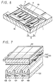
- FIG. 1 is a schematic perspective view showing a main portion of the flat display device
- FIG. 2 is an exploded perspective view showing the main portion
- FIG. 3 is a plan view viewed from a rear surface of the main portion.
- the present invention is not limited to these examples.
- the flat display device of the present invention is constituted so that first and second substrates 1 and 2 which are made of a glass substrate, for example, oppose each other, and, not shown, surroundings of both the substrates 1 and 2 are sealed airtightly by a frit seal or the like.
- This example relates to the case where luminous display is observed from a side of the first substrate 1, and in this case, at least this first substrate 1 is made of a transparent glass substrate, for example, through which a display light is transmitted.
- a discharge maintaining electrode group 5 which is constituted such that plural pairs of discharge maintaining electrodes 3 and 4 which are made of transparent electroconductive layers such as ITO (indium tin oxide) are disposed in parallel in a stripe form, for example, with their mainly extended direction defined as a first direction along the surface of the substrate 1, namely, a direction X in the diagram, is provided on an inner surface of the first substrate 1.
- ITO indium tin oxide
- Counter spacing between the electrodes 3 and 4 are set to less than 50 ⁇ m where cathode glow discharge is possible, and preferably not more than 20 ⁇ m.
- bus electrodes 3b and 4b which are made of Al, for example, with excellent electroconductivity for compensating for the electroconductivity of the discharge maintaining electrodes 3 and 4, are deposited along the mainly extended direction of the discharge maintaining electrodes.
- projecting bar portions 6y which cross the discharge maintaining electrodes 3 and 4 are extended to a second direction Y perpendicularly intersecting the direction X, are formed in parallel at predetermined spacing, and simultaneously intersecting projecting bar portions 6x which cross the projecting bar portions 6y and are extended to the direction X, are formed so that a grid-state projecting bars 6 are formed on the first substrate 1.
- the crossing projecting portions 6x are formed between pairs of discharge maintaining electrodes so as to or not to partially straddle the discharge maintaining electrodes 3 and 4.
- a dielectric layer 7 is deposited onto a whole inner surface of the first substrate 1 with a thickness which is not more than half of spacing between the discharge maintaining electrodes 3 and 4, and a surface layer 8, which has small work function and protects the electrodes and is made of MgO, for example, is formed thereonto.
- the projecting walls 9 are formed at a pitch which is 1/2 of the pitch of the projecting bar portions 6y.
- address electrodes 10 are deposited in a stripe form on the extended direction of top portions of the projecting walls 9, particularly, top portions of projecting walls 9c positioned between the projecting bar portions 6y so that an address electrode group 11 is formed.
- the projecting walls 9 and the projecting bar portion 6 are made to come in contact with each other or join each other and their height is determined so that the spacing between the first and second substrates 1 and 2 as well as the spacing between the address electrodes 10 and the discharge maintaining electrode 3 or 4 which becomes a discharge starting electrode are set to less than 50 ⁇ m, preferably not more than 20 ⁇ m, namely, these spacing are set so that the cathode glow discharge is possible, and namely, the cathode glow discharge takes place.
- Fluorescent layers which emit lights of the same color are formed respectively on both sides of each of the projecting walls 9c on which each of the address electrodes 10 is formed.
- a fluorescent material R which emits a red light is provided in a groove portion between both the projecting walls 9 on both sides of one protruded wall 9c
- a fluorescent material B which emits a blue light and a fluorescent material G which emits a green light are provided respectively in groove portions respectively between another adjacent projecting walls 9c and the protruded wall 9 on both the sides of the protruded wall 9c.
- the discharge is captured by cooperation of the projecting bar portions 6 and the projecting walls 9 on the first and second substrates 1 and 2 so that discharge areas which are separated from another one are formed, and in these areas pixel areas where lights of respective colors are emitted are formed.
- An airtight space formed by the first and second substrates 1 and 2 is evacuated and necessary gas, i.e., one or more kinds of gas selected from He, Ne, Ar, Xe and Kr, for example, such as mixed gas of Ne and Xe, namely, so-called Penning gas is sealed into the airtight space under air pressure of 0.05 to 5.0, for example.
- gas circulating section which does not exert influence of the discharge on another portion can be formed so that the discharge areas can be evacuated and gas can be sealed smoothly.
- the cathode glow discharge is utilized, namely, the cathode glow discharge is mainly utilized, namely, the spacing of a pair of the discharge maintaining electrodes can be set to less than 50 ⁇ m, preferably not more than 20 ⁇ m, the pixel pitch can be reduced, and high-definition and high-density display can be executed.
- the driving power can be reduced more than the case of negative glow discharge, and particularly the power consumption which becomes a problem in the large- screen display can be reduced.
- the transparent glass substrate 1, for example, is prepared, and the discharge maintaining electrodes 3 and 4 are formed on the inner surface of the substrates 1.
- a transparent electroconductive layer such as ITO is deposited on the whole inner surface of the substrate 1 as thick as about 300 nm, for example, and the transparent electroconductive layer is pattern- etched by photolithography so that the discharge maintaining electrodes 3 and 4 with necessary patterns are formed.
- a photoresist layer is applied to ITO formed on the whole surface and baked, and is exposed and developed with the predetermined pattern so that an aimed etching mask which is disposed in parallel is formed. Then, this etching mask is used so that the transparent electroconductive layer is pattern- etched by an etching solution made of a mixed solution of hydrochloric acid and ferric chloride, and the discharge maintaining electrodes 3 and 4 are formed.
- the bus electrodes 3b and 4b are fonned.
- a material with excellent electroconductivity such as Al is vapor-evaporated on the whole inner surface of the first substrate 1 into as thick as about 1 ⁇ m so as to cover the discharge maintaining electrodes 3 and 4.
- the above- mentioned pattern etching is executed by means of photolithography by using phosphoric acid as an etching solution so that the bus electrodes 3b and 4b are formed on the discharge maintaining electrodes 3 and 4 so as to cover a partial width of the electrodes 3 and 4.
- the grid-state projecting bars 6 which are constituted by the projecting bar portions 6y and the intersecting projecting bar portions 6x are formed by a printing method, for example, in a height of 20 ⁇ m and a width of 30 ⁇ m to 40 ⁇ m, for example.
- the dielectric layer 7 made of SiO 2 is formed on the whole surface by the CVD (Chemical Vapor Depositions) method or the like, and MgO is vacuum-evaporated thereon as thick as about 0.5 ⁇ m to 1.0 ⁇ m so that the surface layer 8 is formed.
- CVD Chemical Vapor Depositions
- glass paste is overprinted plural times.
- a thickness per each printing in this case is about 10 ⁇ m, and this printing is repeated so that stripe printing at a height (thickness) of 50 ⁇ m to 80 ⁇ m is executed.
- baking at 500°C to 600°C, for example, is executed.
- the projecting walls 9 at a height of 30 ⁇ m to 60 ⁇ m can be formed.
- the electroconductive layer is formed on top portions of at least every other projecting walls 9c of the projecting walls 9.
- an electroconductive material such as Al is deposited from the diagonally upper direction X along the paper surface to the projecting walls 9 formed along the direction Y perpendicularly intersecting the paper surface of FIG. 4A according to the vacuum evaporation method, for example, having directional property in a direction where the electroconductive material flies, namely, so-called diagonal vacuum evaporation.
- the electroconductive material 12 which is separated from the electroconductive material 12 of the projecting walls 9 on both sides of the projecting walls 9c, is deposited on the every other projecting walls 9c so that the address electrodes 10 can be formed respectively on the projecting walls 9c by the separated electroconductive material 12.
- the similar diagonal vacuum evaporation is executed from diagonally above on the opposite side to FIG. 4A so that the electroconductive material 12 can be formed thicker.
- the electroconductive material 12 on the projecting walls 9 other than the projecting walls 9c can be removed by pattern etching utilizing photolithography, but the electroconductive material 12 can remain on all the projecting walls 9.
- photosensitive fluorescent slurry having fluorescent materials of respective colors is applied and baked successively into the grooves between the adjacent projecting walls 9 which sandwich the respective projecting walls 9c repeatedly.
- the red, green and blue fluorescent materials R, G and B are deposited on both sides sandwiching the respective projecting walls 9c so that the fluorescent surfaces are formed.
- a surface layer 13 made of MgO or the like (not shown in FIG. 2) is formed on the whole surface.
- the second substrate 2 is fabricated.
- first and second substrates 1 and 2 are made to oppose each other in the above-mentioned positional relationship, and are frit-sealed, and they are evacuated and gas is sealed thereinto so that the objective flat display device is formed.
- the end portions of the bus electrodes 3b and 4b and the end portions of the address electrodes 10 are led out to the end portions of the substrates 1 and 2 which extend out of the airtight space so as to be used as feed terminals which are led to the discharge maintaining electrodes 3 and 4 and the address electrodes 10.
- the address electrodes 10 in the case where the address electrodes are deposited on the top portions of the projecting walls 9c by the diagonally vacuum evaporation, the address electrodes 10 can be separated from each other easily.
- the method of forming the address electrodes 10 in the device of the present invention is not limited to the above-mentioned vacuum evaporation method utilizing diagonal flying, and a method of depositing on the whole surface and removing from the groove bottom portions by means of the pattern etching utilizing photolithography can be adopted.
- the glass paste is pattern-printed repeatedly, namely, overprinted so that the projecting walls 9 are formed.
- the glass paste is printed on the whole surface as thick as 50 ⁇ m to 80 ⁇ m and is dried, and a photosensitive film is laminated on the whole surface so as to be exposed and baked into a parallel stripe form, and is developed. Thereafter, the photosensitive film is sandblasted as a mask so that unnecessary glass layer portion is removed, and the photosensitive film is removed and baking is executed at 500°C to 600°C so that the projecting walls 9 at a predetermined height can be formed.
- the heat treatment at a high temperature is given and thus the first and second substrates 1 and 2 contract, and as a result, as shown in FIGS. 5A and 5B, for example, the projecting walls 9 are occasionally displaced from the projecting bar portions 6y.
- the spacing between the substrates 1 and 2, namely, the spacing between the address electrodes 10 and the discharge maintaining electrodes 3 and 4 can set to predetermined spacing, namely, to less than 50 ⁇ m, preferably not more than 20 ⁇ m.
- the present invention is not limited to the above- mentioned example, and, for example, the mainly extended direction of the discharge maintaining electrodes 3 and 4 is the direction X, but as shown in FIG. 6, the pattern of their countered portion can be a zig-zag pattern for lengthening the countered length.
- first and second substrates can be composed of the whole surface and rear panel constituting the airtight flat container constituting the flat display device, or can be constituted by countered substrates which are disposed in the airtight flat container. Namely, various modifications and changes can be made.
- the spacing between the electrodes can be set to be narrow, i.e., to less than 50 ⁇ m, preferably not more than 20 ⁇ m.
- the pixel pitch can be reduced, and thus the high- definition and high-density display can be executed.
- the present invention is constituted by a discharge mode mainly utilizing the cathode glow discharge, the driving power can be reduced further than the case of the negative glow discharge, and particularly the electricity-saving effect on the large-screen display can be improved.
- the lead glass contracts greatly due to the heat treatment in the fabricating steps. This contraction occurs in a state such that the glass of 10 cm is contracted to 20 ⁇ m to 30 ⁇ m in the heat treatment at several 100°C. Furthermore, its dispersion is great per product, and this contraction is different between a center portion and a peripheral portion of the screen. Moreover, in the case where the step of forming the electrodes of plural patterns is executed in one substrate, location of an exposure mask or the like in the pattern etching is displaced on respective portions, and the dispersion occurs per product.
- the distance between the discharge electrodes is set to less than 50 ⁇ m, preferably not more than 20 ⁇ m particularly for the cathode glow discharge, high accuracy is required particularly for its dimension accuracy, and thus there arise problems of yielding and reliability.
- the pair of discharge maintaining electrodes are formed on the first substrate 1 and the address electrodes are formed on the second substrate 2, the pair of discharge maintaining electrodes are formed in the same step, and the address electrodes are formed on the second substrate 2 which is the different side where the discharge maintaining electrodes are formed.
- the spacing between the address electrodes and the discharge maintaining electrodes and the spacing between the discharge maintaining electrodes can be set to the aimed spacing with high accuracy.
- the spacing between the substrates 1 and 2 namely, the spacing between the address electrodes and the discharge maintaining electrodes can be maintained at the predetermined spacing.
- the fabricating method of the present invention when the projecting walls 9 are formed on the second substrate and address electrodes are formed on the top portions of the projecting walls 9 by diagonal flying, the electroconductive material can be formed isolatedly on the top portions of the projecting walls 9. As a result, a step of separating the electroconductive material between the projecting walls is omitted, and the fabrication is simplified.
Landscapes
- Engineering & Computer Science (AREA)
- Physics & Mathematics (AREA)
- Plasma & Fusion (AREA)
- Chemical & Material Sciences (AREA)
- Materials Engineering (AREA)
- Manufacturing & Machinery (AREA)
- Gas-Filled Discharge Tubes (AREA)
Applications Claiming Priority (4)
| Application Number | Priority Date | Filing Date | Title |
|---|---|---|---|
| JP10708599 | 1999-04-14 | ||
| JP10708599 | 1999-04-14 | ||
| JP22934099A JP4106823B2 (ja) | 1999-04-14 | 1999-08-13 | 平面型表示装置とその製造方法 |
| JP22934099 | 1999-08-13 |
Publications (1)
| Publication Number | Publication Date |
|---|---|
| EP1052671A1 true EP1052671A1 (fr) | 2000-11-15 |
Family
ID=26447156
Family Applications (1)
| Application Number | Title | Priority Date | Filing Date |
|---|---|---|---|
| EP00401048A Withdrawn EP1052671A1 (fr) | 1999-04-14 | 2000-04-14 | Dispositif d'affichage plat et son procédé de fabrication |
Country Status (4)
| Country | Link |
|---|---|
| US (1) | US6518702B1 (fr) |
| EP (1) | EP1052671A1 (fr) |
| JP (1) | JP4106823B2 (fr) |
| KR (1) | KR20010014721A (fr) |
Cited By (1)
| Publication number | Priority date | Publication date | Assignee | Title |
|---|---|---|---|---|
| WO2002054437A1 (fr) * | 2000-12-28 | 2002-07-11 | Sony Corporation | Afficheur plasma a alimentation en courant alternatif et son procede de fabrication |
Families Citing this family (5)
| Publication number | Priority date | Publication date | Assignee | Title |
|---|---|---|---|---|
| US6635992B1 (en) * | 1998-12-01 | 2003-10-21 | Toray Industries, Inc. | Board for plasma display with ribs, plasma display and production process therefor |
| US6870315B2 (en) * | 2000-07-21 | 2005-03-22 | Toray Industries, Inc. | Board for plasma display with barrier ribs, plasma display and production process therefor |
| US20030153233A1 (en) * | 2001-01-29 | 2003-08-14 | Yoshifumi Amano | Front side glass substrate for display and display device |
| JP2002270100A (ja) * | 2001-03-12 | 2002-09-20 | Sony Corp | プラズマ放電表示装置 |
| KR20030060171A (ko) * | 2002-01-07 | 2003-07-16 | 삼성에스디아이 주식회사 | 백라이트 장치 |
Citations (3)
| Publication number | Priority date | Publication date | Assignee | Title |
|---|---|---|---|---|
| EP0554172A1 (fr) * | 1992-01-28 | 1993-08-04 | Fujitsu Limited | Dispositif d'affichage à plasma en couleurs du type à décharge de surface |
| EP0823722A2 (fr) * | 1996-08-06 | 1998-02-11 | Hitachi, Ltd. | Panneau d'affichage à décharge gazeuse et dispositif d'affichage |
| EP0996138A2 (fr) * | 1998-10-23 | 2000-04-26 | Sony Corporation | Dispositif d'affichage plat à décharge plasma et procédé de commande dudit dispositif |
Family Cites Families (1)
| Publication number | Priority date | Publication date | Assignee | Title |
|---|---|---|---|---|
| CA2149289A1 (fr) * | 1994-07-07 | 1996-01-08 | Technology Trade And Transfer Corporation | Appareil d'affichage de la decharge |
-
1999
- 1999-08-13 JP JP22934099A patent/JP4106823B2/ja not_active Expired - Fee Related
-
2000
- 2000-04-12 US US09/547,794 patent/US6518702B1/en not_active Expired - Fee Related
- 2000-04-12 KR KR1020000019183A patent/KR20010014721A/ko not_active Withdrawn
- 2000-04-14 EP EP00401048A patent/EP1052671A1/fr not_active Withdrawn
Patent Citations (3)
| Publication number | Priority date | Publication date | Assignee | Title |
|---|---|---|---|---|
| EP0554172A1 (fr) * | 1992-01-28 | 1993-08-04 | Fujitsu Limited | Dispositif d'affichage à plasma en couleurs du type à décharge de surface |
| EP0823722A2 (fr) * | 1996-08-06 | 1998-02-11 | Hitachi, Ltd. | Panneau d'affichage à décharge gazeuse et dispositif d'affichage |
| EP0996138A2 (fr) * | 1998-10-23 | 2000-04-26 | Sony Corporation | Dispositif d'affichage plat à décharge plasma et procédé de commande dudit dispositif |
Cited By (1)
| Publication number | Priority date | Publication date | Assignee | Title |
|---|---|---|---|---|
| WO2002054437A1 (fr) * | 2000-12-28 | 2002-07-11 | Sony Corporation | Afficheur plasma a alimentation en courant alternatif et son procede de fabrication |
Also Published As
| Publication number | Publication date |
|---|---|
| JP4106823B2 (ja) | 2008-06-25 |
| JP2000357461A (ja) | 2000-12-26 |
| KR20010014721A (ko) | 2001-02-26 |
| US6518702B1 (en) | 2003-02-11 |
Similar Documents
| Publication | Publication Date | Title |
|---|---|---|
| US7282860B2 (en) | Plasma display panel with a dielectric layer having depressions between projections and forming ventilation paths | |
| KR100812875B1 (ko) | 플라즈마 디스플레이 장치 | |
| US6518702B1 (en) | Flat display device and fabricating method of the same | |
| EP1069590A1 (fr) | Dispositif d'affichage plat à décharge plasma et procédé de fabrication dudit dispositif | |
| US6512499B1 (en) | Flat plasma discharge display device | |
| US6329749B1 (en) | Planar type plasma discharge display device | |
| KR100653667B1 (ko) | 플라즈마 디스플레이 장치 | |
| EP1045421B1 (fr) | Dispositif d'affichage plat et son procédé de fabrication | |
| US6541913B1 (en) | Flat display apparatus | |
| JP3943650B2 (ja) | 表示用放電管 | |
| JP4375113B2 (ja) | プラズマディスプレイパネル | |
| JP2000123741A (ja) | 表示用放電管 | |
| JP3090079B2 (ja) | カラープラズマディスプレイパネル | |
| EP1071111A1 (fr) | Dispositif d'affichage plat à décharge plasma et procédé de production dudit dispositif | |
| KR200292010Y1 (ko) | 플라즈마표시소자의정합용마아킹 | |
| JP4259190B2 (ja) | プラズマディスプレイパネルの製造方法 | |
| US20090021165A1 (en) | Plasma display panel and method of manufacturing the same | |
| JP2004288401A (ja) | 平板型表示装置 | |
| JP2002163989A (ja) | プラズマディスプレイパネル及びその製造方法 | |
| KR20020062135A (ko) | 가스 방전 표시장치 | |
| KR20080044660A (ko) | 플라즈마 디스플레이 패널 및 그 제조 방법 | |
| WO2003019601A1 (fr) | Structure de la base d'ecrans au plasma, leur procede de fabrication et structure d'ecrans au plasma | |
| JP2008198520A (ja) | プラズマディスプレイパネル及びその製造方法 |
Legal Events
| Date | Code | Title | Description |
|---|---|---|---|
| PUAI | Public reference made under article 153(3) epc to a published international application that has entered the european phase |
Free format text: ORIGINAL CODE: 0009012 |
|
| AK | Designated contracting states |
Kind code of ref document: A1 Designated state(s): DE FR GB |
|
| AX | Request for extension of the european patent |
Free format text: AL;LT;LV;MK;RO;SI |
|
| 17P | Request for examination filed |
Effective date: 20010423 |
|
| AKX | Designation fees paid |
Free format text: DE FR GB |
|
| 17Q | First examination report despatched |
Effective date: 20040123 |
|
| STAA | Information on the status of an ep patent application or granted ep patent |
Free format text: STATUS: THE APPLICATION IS DEEMED TO BE WITHDRAWN |
|
| 18D | Application deemed to be withdrawn |
Effective date: 20040604 |