EP1052732A2 - Einpresskontakt - Google Patents
Einpresskontakt Download PDFInfo
- Publication number
- EP1052732A2 EP1052732A2 EP00105776A EP00105776A EP1052732A2 EP 1052732 A2 EP1052732 A2 EP 1052732A2 EP 00105776 A EP00105776 A EP 00105776A EP 00105776 A EP00105776 A EP 00105776A EP 1052732 A2 EP1052732 A2 EP 1052732A2
- Authority
- EP
- European Patent Office
- Prior art keywords
- pin
- thick film
- polymer thick
- substrate
- hole
- Prior art date
- Legal status (The legal status is an assumption and is not a legal conclusion. Google has not performed a legal analysis and makes no representation as to the accuracy of the status listed.)
- Withdrawn
Links
Images
Classifications
-
- F—MECHANICAL ENGINEERING; LIGHTING; HEATING; WEAPONS; BLASTING
- F21—LIGHTING
- F21V—FUNCTIONAL FEATURES OR DETAILS OF LIGHTING DEVICES OR SYSTEMS THEREOF; STRUCTURAL COMBINATIONS OF LIGHTING DEVICES WITH OTHER ARTICLES, NOT OTHERWISE PROVIDED FOR
- F21V21/00—Supporting, suspending, or attaching arrangements for lighting devices; Hand grips
- F21V21/08—Devices for easy attachment to any desired place, e.g. clip, clamp, magnet
-
- H—ELECTRICITY
- H01—ELECTRIC ELEMENTS
- H01R—ELECTRICALLY-CONDUCTIVE CONNECTIONS; STRUCTURAL ASSOCIATIONS OF A PLURALITY OF MUTUALLY-INSULATED ELECTRICAL CONNECTING ELEMENTS; COUPLING DEVICES; CURRENT COLLECTORS
- H01R12/00—Structural associations of a plurality of mutually-insulated electrical connecting elements, specially adapted for printed circuits, e.g. printed circuit boards [PCB], flat or ribbon cables, or like generally planar structures, e.g. terminal strips, terminal blocks; Coupling devices specially adapted for printed circuits, flat or ribbon cables, or like generally planar structures; Terminals specially adapted for contact with, or insertion into, printed circuits, flat or ribbon cables, or like generally planar structures
- H01R12/50—Fixed connections
- H01R12/51—Fixed connections for rigid printed circuits or like structures
- H01R12/55—Fixed connections for rigid printed circuits or like structures characterised by the terminals
- H01R12/58—Fixed connections for rigid printed circuits or like structures characterised by the terminals terminals for insertion into holes
-
- H—ELECTRICITY
- H05—ELECTRIC TECHNIQUES NOT OTHERWISE PROVIDED FOR
- H05K—PRINTED CIRCUITS; CASINGS OR CONSTRUCTIONAL DETAILS OF ELECTRIC APPARATUS; MANUFACTURE OF ASSEMBLAGES OF ELECTRICAL COMPONENTS
- H05K3/00—Apparatus or processes for manufacturing printed circuits
- H05K3/30—Assembling printed circuits with electric components, e.g. with resistors
- H05K3/306—Assembling printed circuits with electric components, e.g. with resistors with lead-in-hole components
- H05K3/308—Adaptations of leads
-
- H—ELECTRICITY
- H05—ELECTRIC TECHNIQUES NOT OTHERWISE PROVIDED FOR
- H05K—PRINTED CIRCUITS; CASINGS OR CONSTRUCTIONAL DETAILS OF ELECTRIC APPARATUS; MANUFACTURE OF ASSEMBLAGES OF ELECTRICAL COMPONENTS
- H05K2201/00—Indexing scheme relating to printed circuits covered by H05K1/00
- H05K2201/09—Shape and layout
- H05K2201/09818—Shape or layout details not covered by a single group of H05K2201/09009 - H05K2201/09809
- H05K2201/09981—Metallised walls
-
- H—ELECTRICITY
- H05—ELECTRIC TECHNIQUES NOT OTHERWISE PROVIDED FOR
- H05K—PRINTED CIRCUITS; CASINGS OR CONSTRUCTIONAL DETAILS OF ELECTRIC APPARATUS; MANUFACTURE OF ASSEMBLAGES OF ELECTRICAL COMPONENTS
- H05K2201/00—Indexing scheme relating to printed circuits covered by H05K1/00
- H05K2201/10—Details of components or other objects attached to or integrated in a printed circuit board
- H05K2201/10227—Other objects, e.g. metallic pieces
- H05K2201/10295—Metallic connector elements partly mounted in a hole of the PCB
- H05K2201/10303—Pin-in-hole mounted pins
-
- H—ELECTRICITY
- H05—ELECTRIC TECHNIQUES NOT OTHERWISE PROVIDED FOR
- H05K—PRINTED CIRCUITS; CASINGS OR CONSTRUCTIONAL DETAILS OF ELECTRIC APPARATUS; MANUFACTURE OF ASSEMBLAGES OF ELECTRICAL COMPONENTS
- H05K2201/00—Indexing scheme relating to printed circuits covered by H05K1/00
- H05K2201/10—Details of components or other objects attached to or integrated in a printed circuit board
- H05K2201/10431—Details of mounted components
- H05K2201/1059—Connections made by press-fit insertion
-
- H—ELECTRICITY
- H05—ELECTRIC TECHNIQUES NOT OTHERWISE PROVIDED FOR
- H05K—PRINTED CIRCUITS; CASINGS OR CONSTRUCTIONAL DETAILS OF ELECTRIC APPARATUS; MANUFACTURE OF ASSEMBLAGES OF ELECTRICAL COMPONENTS
- H05K2201/00—Indexing scheme relating to printed circuits covered by H05K1/00
- H05K2201/10—Details of components or other objects attached to or integrated in a printed circuit board
- H05K2201/10613—Details of electrical connections of non-printed components, e.g. special leads
- H05K2201/10742—Details of leads
- H05K2201/1075—Shape details
- H05K2201/10871—Leads having an integral insert stop
-
- H—ELECTRICITY
- H05—ELECTRIC TECHNIQUES NOT OTHERWISE PROVIDED FOR
- H05K—PRINTED CIRCUITS; CASINGS OR CONSTRUCTIONAL DETAILS OF ELECTRIC APPARATUS; MANUFACTURE OF ASSEMBLAGES OF ELECTRICAL COMPONENTS
- H05K3/00—Apparatus or processes for manufacturing printed circuits
- H05K3/40—Forming printed elements for providing electric connections to or between printed circuits
- H05K3/4038—Through-connections; Vertical interconnect access [VIA] connections
- H05K3/4053—Through-connections; Vertical interconnect access [VIA] connections by thick-film techniques
- H05K3/4069—Through-connections; Vertical interconnect access [VIA] connections by thick-film techniques for via connections in organic insulating substrates
-
- Y—GENERAL TAGGING OF NEW TECHNOLOGICAL DEVELOPMENTS; GENERAL TAGGING OF CROSS-SECTIONAL TECHNOLOGIES SPANNING OVER SEVERAL SECTIONS OF THE IPC; TECHNICAL SUBJECTS COVERED BY FORMER USPC CROSS-REFERENCE ART COLLECTIONS [XRACs] AND DIGESTS
- Y10—TECHNICAL SUBJECTS COVERED BY FORMER USPC
- Y10S—TECHNICAL SUBJECTS COVERED BY FORMER USPC CROSS-REFERENCE ART COLLECTIONS [XRACs] AND DIGESTS
- Y10S439/00—Electrical connectors
- Y10S439/931—Conductive coating
Definitions
- This invention relates to a solderless pin connection utilizing a press fit pin staked within a hole printed with polymer thick film.
- a perceived advantage of copper is its ability to maintain a soldered connection for electrical and mechanical connections. Staking a pin into a multi-processed copper plated through hole may result in a solder-free joint.
- Soldered connections require additional complex and costly manufacturing steps and may result in unreliable connections. Waste from the soldering and plating processes is hazardous to the environment and expensive to dispose of safely. Further, manufacture of the plated through hole requires a lengthy process with many steps, including a drilled hole, that are critical to achieving a sound electrical connection. This lengthy plating process, combined with the assembly of the pin, may jeopardize the integrity of the plated through hole.
- Polymer thick film is a material and process used to create printed circuit boards and other products.
- Polymer thick film is an additive material and process for printed circuit board manufacturing that can improve reliability, product performance and quality and at the same time reduce overall component costs.
- Polymer thick film comprises polymer resins filled with conductive particles that are screen printed and heat cured onto the surface of a printed circuit board substrate.
- a loading ratio can be varied to create materials having variable conductivities, depending on the application.
- the conductive particles can also be blended, such as a silver/carbon mixture, to achieve particular characteristics.
- Polymer thick film inks are used to create variable resistors, fixed resistors, conductors, insulating layers, switches and other devices on the surface of a printed circuit board.
- a solderless pin connection for a printed circuit board is prepared using polymer thick film printed on a printed circuit board substrate.
- An inner surface of the substrate defines a hole, that may be drilled or punched into the substrate.
- the polymer thick film is applied on a top surface of the substrate and along the inner surface. Additionally, the polymer thick film may be applied to a bottom surface of the substrate and in an additional layer along the inner surface.
- a pin is subsequently press fit within the polymer thick film along the inner surface.
- the pin preferably has a pin diameter less than a diameter of the hole.
- the pin is retained within the hole using either the press fit connection, or preferably is staked into the hole using a mechanical connection such as barbs, a folded staked end portion of the pin, a shoulder positioned on the pin and/or teeth positioned on the shoulder.
- the polymer thick film is preferably applied to the substrate by drawing the polymer thick film through the hole and along the inner surface from each side of the substrate. The resultant inner surface of the hole is consistently coated with the polymer thick film.
- a pin connection for a printed circuit board according to this invention is shown and described that does not require copper, a plated through hole or solder.
- polymer thick film 30 is used in connection with the printed circuit board to effectuate such a solderless connection.
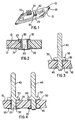
- Printed circuit boards are typically constructed on substrate 10 such as a fiberglass board or other substrate known to those having ordinary skill in the art.
- substrate 10 such as a fiberglass board or other substrate known to those having ordinary skill in the art.
- a printed circuit board may comprise any number of substrates 10 other than fiberglass, including plastic or other materials, because, unlike copper, polymer thick film is appropriate for use with a wide range of substrate materials.
- a representative printed circuit board is shown in Fig. 1.
- hole 25 is drilled or punched in substrate 10 to accommodate a corresponding pin connection.
- Hole 25 extends from top surface 13 of substrate 10 to bottom surface 15 of substrate 10. According to one preferred embodiment of this invention, hole 25 is punched thereby reducing the complexity of the assembly process and enabling a more precise hole position.
- polymer thick film 30 is applied along top surface 13 of substrate 10.
- polymer thick film 30 is applied along top surface 13 and bottom surface 15 of substrate 10.
- a printed circuit board may require printed circuits on one or both sides of substrate 10 in addition to solderless pin connections on one or both sides of substrate 10.
- polymer thick film 30 is applied along inner surface 20 that defines hole 25. Because conventional application equipment applies polymer thick film 30 only along a horizontal or vertical plane, polymer thick film 30 should have a suitable viscosity during the application process to coat inner surface 30.
- polymer thick film 30 is preferably applied to a portion of top surface 13 and bottom surface 15 of substrate 10 surrounding hole 25 and in additionally layered along inner surface 20 that defines hole 25.
- polymer thick film 30 is applied by using a vacuum positioned on one side of substrate 10 and drawing viscous polymer thick film 30 through hole 25. This procedure is then repeated on an opposite side of substrate so that viscous polymer thick film 30 is drawn through hole 25 from each side of substrate 10.
- the resultant hole 25 is preferably coated with a consistent layer of polymer thick film 30 on top surface 13 surrounding hole 25, bottom surface 15 surrounding hole 25 and inner surface 20 within hole 25. Hole 25 coated with polymer thick film 30 in this manner is typically referred to as a printed through hole.
- polymer thick film 30 is often in an ink form.
- the curing process according to one preferred embodiment of this invention involves heating or baking the polymer thick film-coated substrate 10 at a predetermined temperature for a predetermined duration.
- pin 40 is press fit against polymer thick film 30 within hole 25. Pin 40 is preferably retained within hole 25 through the press fit and/or a mechanical connection as described below.
- pin 40 preferably contacts a continuous layer of polymer thick film 30 throughout the entire inner surface 20 of hole 25. Therefore, pin 40 preferably has a pin diameter less than a diameter of hole 25. If pin 40 has a greater pin diameter than a diameter of hole 25 then pin 40 will scrape and push out most or all of polymer thick film 30 coated along inner surface 20 during insertion into hole 25.
- Polymer thick film 30 is preferably blended with a conductive pigment such as a silver or carbon additive. Polymer thick film 30 is preferably manufactured and blended to exhibit specific physical characteristics. Polymer thick film 30 printed through holes have a typical resistance of 100 milliohms or less, and can conduct up to 1 amp per hole.
- a viscosity of the polymer thick film ink as it is applied is important for achieving a reliable printed through hole.
- the viscosity preferably ranges between 16-34 on a viscometer 0-100 scale.
- a hardness of polymer thick film 30 is important to permit insertion of pin 40 into hole 25.
- Polymer thick film 30 should be malleable and preferably conform to a shape of an inserted end of pin 40. Based upon testing with a pencil hardness tester, the hardness of polymer thick film 30 is preferably between 6H and 9H. The hardness of polymer thick film 30 may be varied outside of this range depending upon how pin 40 is staked with respect to substrate 10 and depending upon the desired characteristics of polymer thick film 30.
- Pin 40 may be staked with respect to polymer thick film 30 on inner surface 20 of substrate 10 using one or more mechanical connections. As shown in Figs. 3 and 4, such mechanical connection may comprise barb 45 or other serration for digging or anchoring into polymer thick film 30 on inner surface 20 of substrate 10. Barb 45 may comprise any configuration known to those having ordinary skill in the art tat will allow insertion of pin 40 into hole 25 using some degree of force but prevent accidental removal or loss of pin 40 from hole 25 under ordinary operating conditions.
- pin 40 may comprise folded region 50 staking pin 40 with respect to substrate 10.
- Pin 40 may be inserted into hole 25 and then compressed or bent at a staked end of pin 40 to create an overlapping or folded region 50 of pin 40 with respect to a surface of substrate 10 and/or polymer thick film 30 layered on substrate 10.
- the staked end of pin 40 may be compressed into a nest or similar mechanical device to create folded region 50 of pin 40.
- pin 40 may further comprise shoulder 55.
- shoulder 55 preferably protrudes radially from pin 40 to seat pin 40 firmly and predictably against substrate 10 and polymer thick film 30.
- shoulder 55 further comprises at least one tooth 60 for engaging with substrate 10 and/or polymer thick film 30.
- One or more teeth 60 are especially useful when pin 40 does not have barbs 45 or other mechanical connections on a portion of pin 40 within hole 25.
Landscapes
- Engineering & Computer Science (AREA)
- Manufacturing & Machinery (AREA)
- Microelectronics & Electronic Packaging (AREA)
- General Engineering & Computer Science (AREA)
- Printing Elements For Providing Electric Connections Between Printed Circuits (AREA)
- Multi-Conductor Connections (AREA)
- Electric Connection Of Electric Components To Printed Circuits (AREA)
Applications Claiming Priority (2)
| Application Number | Priority Date | Filing Date | Title |
|---|---|---|---|
| US09/309,353 US6217346B1 (en) | 1999-05-11 | 1999-05-11 | Solderless pin connection |
| US309353 | 1999-05-11 |
Publications (2)
| Publication Number | Publication Date |
|---|---|
| EP1052732A2 true EP1052732A2 (de) | 2000-11-15 |
| EP1052732A3 EP1052732A3 (de) | 2002-03-20 |
Family
ID=23197870
Family Applications (1)
| Application Number | Title | Priority Date | Filing Date |
|---|---|---|---|
| EP00105776A Withdrawn EP1052732A3 (de) | 1999-05-11 | 2000-03-18 | Einpresskontakt |
Country Status (8)
| Country | Link |
|---|---|
| US (1) | US6217346B1 (de) |
| EP (1) | EP1052732A3 (de) |
| JP (1) | JP2000349408A (de) |
| KR (1) | KR100766883B1 (de) |
| CN (1) | CN1253058C (de) |
| AU (1) | AU730065B2 (de) |
| CA (1) | CA2302798C (de) |
| TW (1) | TW488194B (de) |
Cited By (3)
| Publication number | Priority date | Publication date | Assignee | Title |
|---|---|---|---|---|
| WO2003003799A1 (en) * | 2001-06-26 | 2003-01-09 | Teradyne, Inc. | Direct inner layer interconnect for a high speed printed circuit board |
| DE10334581A1 (de) * | 2003-07-28 | 2005-02-24 | Conti Temic Microelectronic Gmbh | Verfahren zur Herstellung einer elektrischen Baugruppe |
| EP3249751A3 (de) * | 2016-05-24 | 2018-02-28 | TE Connectivity Corporation | Einpresssteckverbinder für leiterplatte |
Families Citing this family (20)
| Publication number | Priority date | Publication date | Assignee | Title |
|---|---|---|---|---|
| JP2002023026A (ja) * | 2000-07-07 | 2002-01-23 | Yazaki Corp | 光コネクタ |
| US6552277B1 (en) * | 2000-09-08 | 2003-04-22 | Emc Corporation | Techniques for forming a connection between a pin and a circuit board |
| US6716072B1 (en) | 2002-06-27 | 2004-04-06 | Emc Corporation | Systems and methods for disposing a circuit board component on a circuit board using a soldering pin |
| US6851173B2 (en) | 2002-08-27 | 2005-02-08 | Datech Technology Co., Ltd. | Method for joining metal component by press-fit connection |
| US6773269B1 (en) | 2002-09-27 | 2004-08-10 | Emc Corporation | Circuit board assembly which utilizes a pin assembly and techniques for making the same |
| JP4276881B2 (ja) * | 2003-04-30 | 2009-06-10 | 日本圧着端子製造株式会社 | 多層プリント配線板の接続構造 |
| US7377823B2 (en) * | 2005-05-23 | 2008-05-27 | J.S.T. Corporation | Press-fit pin |
| US7249981B2 (en) | 2005-07-08 | 2007-07-31 | J.S.T. Corporation | Press-fit pin |
| US7537464B2 (en) * | 2006-06-23 | 2009-05-26 | Delphi Technologies, Inc. | Electrical pin interconnection for electronic package |
| US7661997B2 (en) * | 2006-09-12 | 2010-02-16 | Woody Wurster | Pin to CB system |
| JP4993754B2 (ja) * | 2008-02-22 | 2012-08-08 | 新光電気工業株式会社 | Pga型配線基板及びその製造方法 |
| CN103385040A (zh) | 2011-02-25 | 2013-11-06 | 瑞典爱立信有限公司 | 连接引脚和将连接引脚安装于电子组件的部件载体中的方法、以及这种包括连接引脚的部件载体 |
| EP2679081B1 (de) * | 2011-02-25 | 2018-04-11 | Telefonaktiebolaget LM Ericsson (publ) | Verfahren zur montage von verbindungsbolzen bei einem bauteilträger, verbundwerkzeug zur montage von verbindungsbolzen, bauteilträger als modul für eine elektronische baugruppe und eine solche baugruppe |
| US9093775B2 (en) | 2011-02-25 | 2015-07-28 | Telefonaktiebolaget L M Ericsson (Publ) | Connection pin for mounting in a component carrier, a method for producing an electronic assembly comprising a motherboard with stackable modules comprising a component carrier, and such an electronic assembly |
| US8371871B1 (en) * | 2011-08-11 | 2013-02-12 | Advanced Interconnections Corp. | Terminal with compliant barb |
| KR101558743B1 (ko) | 2014-03-04 | 2015-10-07 | 현대자동차주식회사 | 부품 체결력 증대를 위한 전자회로기판용 체결핀 |
| US9595782B2 (en) * | 2015-08-05 | 2017-03-14 | Te Connectivity Corporation | Pin with angled retention member |
| DE102015220688A1 (de) * | 2015-10-22 | 2017-04-27 | Zf Friedrichshafen Ag | Elektrischer Stecker und Verfahren zum Herstellen |
| CN108832450A (zh) * | 2018-05-29 | 2018-11-16 | 大宁县鑫辉电子元件制造有限公司 | 一种矿灯线路板用插针的制作方法 |
| KR102343341B1 (ko) * | 2020-10-05 | 2021-12-27 | 김출곤 | 터치스위치 접지핀 제조방법과 그 접지핀 |
Citations (2)
| Publication number | Priority date | Publication date | Assignee | Title |
|---|---|---|---|---|
| US4327247A (en) * | 1978-10-02 | 1982-04-27 | Shin-Kobe Electric Machinery Co., Ltd. | Printed wiring board |
| EP0825680A2 (de) * | 1996-08-23 | 1998-02-25 | CTS Corporation | Verformbarer elektrischer Verbindungsstift |
Family Cites Families (7)
| Publication number | Priority date | Publication date | Assignee | Title |
|---|---|---|---|---|
| US3912852A (en) * | 1974-05-31 | 1975-10-14 | Westinghouse Electric Corp | Thin-film electrical circuit lead connection arrangement |
| US4181387A (en) * | 1978-06-21 | 1980-01-01 | Western Electric Company, Inc. | Interconnect sockets and assemblies |
| US4230385A (en) * | 1979-02-06 | 1980-10-28 | Elfab Corporation | Printed circuit board, electrical connector and method of assembly |
| US4656314A (en) * | 1982-02-08 | 1987-04-07 | Industrial Science Associates | Printed circuit |
| US4954089A (en) * | 1984-01-18 | 1990-09-04 | Methode Electronics, Inc. | Terminator assembly for interconnecting computer devices |
| TW254004B (en) * | 1993-12-07 | 1995-08-11 | Methode Electronics Inc | Low profile electrical adaptor |
| US5480309A (en) * | 1994-05-23 | 1996-01-02 | Kel Corporation | Universal multilayer base board assembly for integrated circuits |
-
1999
- 1999-05-11 US US09/309,353 patent/US6217346B1/en not_active Expired - Lifetime
-
2000
- 2000-03-18 EP EP00105776A patent/EP1052732A3/de not_active Withdrawn
- 2000-03-28 CA CA002302798A patent/CA2302798C/en not_active Expired - Fee Related
- 2000-04-03 CN CNB001054953A patent/CN1253058C/zh not_active Expired - Fee Related
- 2000-04-12 AU AU27719/00A patent/AU730065B2/en not_active Ceased
- 2000-04-14 KR KR1020000019478A patent/KR100766883B1/ko not_active Expired - Fee Related
- 2000-05-08 TW TW089108861A patent/TW488194B/zh not_active IP Right Cessation
- 2000-05-11 JP JP2000143421A patent/JP2000349408A/ja active Pending
Patent Citations (2)
| Publication number | Priority date | Publication date | Assignee | Title |
|---|---|---|---|---|
| US4327247A (en) * | 1978-10-02 | 1982-04-27 | Shin-Kobe Electric Machinery Co., Ltd. | Printed wiring board |
| EP0825680A2 (de) * | 1996-08-23 | 1998-02-25 | CTS Corporation | Verformbarer elektrischer Verbindungsstift |
Cited By (4)
| Publication number | Priority date | Publication date | Assignee | Title |
|---|---|---|---|---|
| WO2003003799A1 (en) * | 2001-06-26 | 2003-01-09 | Teradyne, Inc. | Direct inner layer interconnect for a high speed printed circuit board |
| US6593535B2 (en) | 2001-06-26 | 2003-07-15 | Teradyne, Inc. | Direct inner layer interconnect for a high speed printed circuit board |
| DE10334581A1 (de) * | 2003-07-28 | 2005-02-24 | Conti Temic Microelectronic Gmbh | Verfahren zur Herstellung einer elektrischen Baugruppe |
| EP3249751A3 (de) * | 2016-05-24 | 2018-02-28 | TE Connectivity Corporation | Einpresssteckverbinder für leiterplatte |
Also Published As
| Publication number | Publication date |
|---|---|
| CA2302798C (en) | 2003-12-23 |
| CN1253058C (zh) | 2006-04-19 |
| KR20010014730A (ko) | 2001-02-26 |
| US6217346B1 (en) | 2001-04-17 |
| KR100766883B1 (ko) | 2007-10-16 |
| AU730065B2 (en) | 2001-02-22 |
| CA2302798A1 (en) | 2000-11-11 |
| TW488194B (en) | 2002-05-21 |
| EP1052732A3 (de) | 2002-03-20 |
| AU2771900A (en) | 2000-11-30 |
| CN1273501A (zh) | 2000-11-15 |
| JP2000349408A (ja) | 2000-12-15 |
Similar Documents
| Publication | Publication Date | Title |
|---|---|---|
| US6217346B1 (en) | Solderless pin connection | |
| AU592627B2 (en) | Printed circuit board capable of preventing electromagnetic interference | |
| US6180221B1 (en) | Conductive elastomer for grafting to thermoplastic and thermoset substrates | |
| KR20010072571A (ko) | 전기 장치 | |
| JPH0850967A (ja) | 印刷プラスチツク回路および接触子とその製法 | |
| US9831575B2 (en) | Press fit electrical terminal having a solder tab shorter than PCB thickness and method of using same | |
| US3202755A (en) | Welded circuit assembly and method of assembly | |
| GB2222917A (en) | Electrical connector for PCB | |
| US4064357A (en) | Interconnected printed circuits and method of connecting them | |
| JP2008078677A (ja) | シールドフレキシブルプリント配線板 | |
| US3447039A (en) | Electronic circuit test board | |
| WO1988010015A1 (en) | A pin fastened to a printed circuit board by soldering | |
| WO2020200464A1 (en) | Method for manufacturing an antenna element | |
| US5839189A (en) | Bracket for attaching pin-in-hole components to a surface mount board | |
| WO2002082874A2 (en) | Pin connector | |
| MXPA00004497A (es) | Conexion o union con pasador sin soldadura | |
| CN210725559U (zh) | 一种用两种方式导通电路板两面的双面电路板 | |
| US20250227854A1 (en) | Coverlay as printed circuit board (pcb) voltage insulator under connectors | |
| JP3454013B2 (ja) | フレキシブル配線基板の端子接続方法 | |
| US20070184688A1 (en) | Interconnection device for a double-sided printed circuit board | |
| US6382988B1 (en) | Encircled electrical compression contact | |
| KR102465243B1 (ko) | 인쇄회로기판 제조 방법 및 이에 의해 제조된 인쇄회로기판 | |
| JP4080417B2 (ja) | エラストマコネクタ | |
| EP1949774A1 (de) | Verfahren zum verbinden von leiterplatten | |
| US20090067145A1 (en) | Circuit pattern designing method, wherein an electroconductive coating material is used, and a printed circuit board |
Legal Events
| Date | Code | Title | Description |
|---|---|---|---|
| PUAI | Public reference made under article 153(3) epc to a published international application that has entered the european phase |
Free format text: ORIGINAL CODE: 0009012 |
|
| AK | Designated contracting states |
Kind code of ref document: A2 Designated state(s): AT BE CH CY DE DK ES FI FR GB GR IE IT LI LU MC NL PT SE |
|
| AX | Request for extension of the european patent |
Free format text: AL;LT;LV;MK;RO;SI |
|
| 17P | Request for examination filed |
Effective date: 20010324 |
|
| PUAL | Search report despatched |
Free format text: ORIGINAL CODE: 0009013 |
|
| AK | Designated contracting states |
Kind code of ref document: A3 Designated state(s): AT BE CH CY DE DK ES FI FR GB GR IE IT LI LU MC NL PT SE |
|
| AX | Request for extension of the european patent |
Free format text: AL;LT;LV;MK;RO;SI |
|
| AKX | Designation fees paid |
Free format text: AT BE CH CY DE DK ES FI FR GB GR IE IT LI LU MC NL PT SE |
|
| 17Q | First examination report despatched |
Effective date: 20060328 |
|
| 17Q | First examination report despatched |
Effective date: 20060328 |
|
| 17Q | First examination report despatched |
Effective date: 20060328 |
|
| GRAP | Despatch of communication of intention to grant a patent |
Free format text: ORIGINAL CODE: EPIDOSNIGR1 |
|
| STAA | Information on the status of an ep patent application or granted ep patent |
Free format text: STATUS: THE APPLICATION IS DEEMED TO BE WITHDRAWN |
|
| 18D | Application deemed to be withdrawn |
Effective date: 20070616 |