EP1052771A2 - Eine hochfrequenzsignalverstärkende Schaltung und Empfänger mit einer solchen Schaltung - Google Patents
Eine hochfrequenzsignalverstärkende Schaltung und Empfänger mit einer solchen Schaltung Download PDFInfo
- Publication number
- EP1052771A2 EP1052771A2 EP00303826A EP00303826A EP1052771A2 EP 1052771 A2 EP1052771 A2 EP 1052771A2 EP 00303826 A EP00303826 A EP 00303826A EP 00303826 A EP00303826 A EP 00303826A EP 1052771 A2 EP1052771 A2 EP 1052771A2
- Authority
- EP
- European Patent Office
- Prior art keywords
- transistor
- input
- high frequency
- frequency signal
- circuit
- Prior art date
- Legal status (The legal status is an assumption and is not a legal conclusion. Google has not performed a legal analysis and makes no representation as to the accuracy of the status listed.)
- Withdrawn
Links
Images


Classifications
-
- H—ELECTRICITY
- H03—ELECTRONIC CIRCUITRY
- H03G—CONTROL OF AMPLIFICATION
- H03G3/00—Gain control in amplifiers or frequency changers
- H03G3/20—Automatic control
- H03G3/30—Automatic control in amplifiers having semiconductor devices
- H03G3/3036—Automatic control in amplifiers having semiconductor devices in high-frequency amplifiers or in frequency-changers
-
- H—ELECTRICITY
- H03—ELECTRONIC CIRCUITRY
- H03G—CONTROL OF AMPLIFICATION
- H03G1/00—Details of arrangements for controlling amplification
- H03G1/0005—Circuits characterised by the type of controlling devices operated by a controlling current or voltage signal
- H03G1/0017—Circuits characterised by the type of controlling devices operated by a controlling current or voltage signal the device being at least one of the amplifying solid-state elements
- H03G1/0023—Circuits characterised by the type of controlling devices operated by a controlling current or voltage signal the device being at least one of the amplifying solid-state elements in emitter-coupled or cascode amplifiers
Definitions
- This invention relates to a high frequency signal amplifying circuit, and a receiver for a broadcast, for example the DAB (Digital Audio Broadcasting) system to which the high frequency signal amplifying circuit is applied.
- DAB Digital Audio Broadcasting
- Broadcasting waves received by an antenna 1 are supplied to a front-end section which includes a high frequency signal amplifying circuit 2 as shown in Fig.3.
- a received signal is supplied to a mixing circuit 3 after amplified by the high frequency signal amplifying circuit 2.
- This amplified signal from the high frequency signal amplifying circuit 2 is then frequency-converted at this mixing circuit 3 into an intermediate frequency signal by a local oscillation signal supplied from a local oscillation circuit 4.
- intermediate frequency signal from the mixing circuit 3 is then amplified at an intermediate frequency signal amplifying circuit 5 by about 60 dB, and then demodulated at a demodulation circuit 6.
- a demodulated signal from the demodulation circuit 6 is supplied to an A/D (Analog to Digital) converter 7.
- A/D Analog to Digital
- a signal level of the demodulated signal from the demodulation circuit 6 is adjusted to be about 1V p-p signal level that is required by the A/D converter 7 as an input level.
- a digital signal from the A/D converter 7 is supplied to a base-band processing circuit 8, and after being digitally demodulated at this base-band processing circuit 8, a digitally demodulated signal from the base-band processing circuit 8 is then supplied to a D/A (Digital to Analog) converter 9.
- D/A Digital to Analog
- the digitally demodulated signal is converted into an analog audio signal, and finally derived from a speaker 10 as an audio sound.
- an AGC Automatic Gain Control circuit 11 connected to the intermediate frequency signal amplifying circuit 5 starts its operation and controls operation of the high frequency signal amplifying circuit 2.
- AGC Automatic Gain Control
- the received signal becomes distorted.
- a gain of the high frequency signal amplifying circuit 2 is controlled to reduce the level of the received signal.
- the OFDM (Orthogonal Frequency Division Multiplex) system is employed to a modulation system of the DAB system.
- a feature of this OFDM system is to employ a multi-carrier system that carries out demodulation while receiving simultaneously plural carriers.
- the DAB mode 2 384 kinds of carriers are transmitted in a transmission bandwidth of 1.536 MHz with the space of 4kHz.
- a high frequency signal amplifying circuit is required to have a low distortion characteristics such as the IM3 > 50dBc, wherein the IM3 means the third inter modulation distortion.
- IM Inter Modulation
- level differences between the level of the input signals (F1) and the distortion signals (F1-Fd) are called as the IM3.
- the DAB receiver is required to have a high frequency signal amplifying circuit having high linearity and being equipped with a gain control circuit upon operating at high frequency.
- the high frequency signal amplifying circuit 2 for the DAB receiver requires to be controlled its gain in accordance with signal strength of the received signal, and requires to operate with low distortion and low noise characteristics.
- the DAB receiver for an auto-mobile use is appeared on the market, and in order to satisfy above-mentioned requirements, the high frequency signal amplifying circuit 2 of the DAB receiver employs a construction including an attenuation circuit such as a PIN diode at the front-end section.
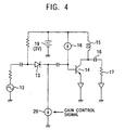
- Fig.4 shows one example of a gain-controllable high frequency signal amplifying circuit used in the conventional DAB receiver.
- an input signal source 12 supplies the received signal in the above-mentioned example in Fig.3, and the received signal from this input signal source 12 is amplified by an npn transistor 14 after passing through a PIN diode 13.
- the input signal source 12 may include a pre-stage circuit instead of the antenna 1.
- the signal from the npn transistor 14 is then obtained through a load inductor 15 and a load capacitor 16 at an output end 17 as an amplified signal.
- a current source 18 is used for supplying a base bias current to the npn transistor 14. Further, a voltage of a DC (Direct Current) voltage source 19 is 3volts in this example, and resultantly, 5mA of the base bias current is supplied to the a base electrode of the npn transistor 14 from the current source 18.
- DC Direct Current
- a current source 20 is an AGC current source in which current value is controlled by a gain control signal from the AGC circuit 11 in Fig.3.
- the current source 20 flows current of about 10mA when the level of the received signal is below a predetermined level. In this condition, an On resistance value of the PIN diode 13 is low or almost zero, thereby the received signal from the input signal source 12 is supplied to the npn transistor 14 without attenuation.
- the current value of the current source 20 is reduced by the gain control signal from the AGC circuit 11. Then the resistance value of the PIN diode 13 goes high, and thereby, the received signal supplied from the PIN diode 13 to the npn transistor 14 is attenuated at this PIN diode 13 and the gain of the high frequency signal amplifying circuit in Fig.4 is lowered.
- the high frequency signal amplifying circuit in Fig.4 is gain-controlled to make the level of the amplified signal to be supplied to the mixing circuit 3 to be a proper value in accordance with the gain control signal from the AGC circuit 11.
- the high frequency signal amplifying circuit in Fig.4 for the auto mobile DAB receiver is not suitable for a portable radio receiver because of following problems. Namely,
- a high frequency signal amplifying circuit of this invention comprises, an input npn transistor to be supplied a high frequency input signal to its base electrode, an output npn transistor cascade-connected to said input npn transistor for obtaining an amplified signal of said high frequency input signal at a collector electrode of this output npn transistor, a bias circuit for controlling a base current of said input npn transistor by detecting direct current components within currents flowing through the cascade-connected two npn transistors, and a shunt transistor having an emitter electrode connected to the base electrode of said input npn transistor, a collector electrode connected to one terminal of a power source, and a resister connected between the base electrode and the emitter electrode of the shunt transistor in order to flow said base current from said bias circuit.
- a gain of the high frequency signal amplifying circuit comprised of the cascade-connected two npn transistors are lowered by reducing a base voltage of the output npn transistor in accordance with a gain control signal, and accordingly collector currents of said input transistor are reduced, and simultaneously the shunt transistor is made in shunt operation.
- the input signal is amplified by the cascade-connected two transistors. And a DC current of the predetermined value is flowed through this cascade-connected two transistors due to the operation of the bias circuit.
- the input npn transistor becomes into saturated condition when a voltage between the collector and the emitter of the input transistor is lowered by the reduction of base voltage of the output npn transistor due to the gain control signal.
- the shunt transistor flows shunt currents due to the increase of the base current owing to the saturation of the output npn transistor, thereby the input signal becomes small to be supplied to the amplifying section comprised of two npn transistors. Accordingly both a control for reducing gain of the amplifying circuit and a control for lowering the input signal by shunting the input section of the amplifying circuit are simultaneously operated.
- the DAB receiver of this invention employs a high frequency signal amplifying circuit which comprises, an input npn transistor to be supplied a high frequency input signal to its base electrode, an output npn transistor cascade-connected to the input npn transistor for obtaining an amplified signal of the high frequency input signal at a collector electrode of this output npn transistor, a bias circuit for controlling a base current of the input npn transistor to be a constant value by detecting direct current components within currents flowing through the cascade-connected two npn transistors, and a shunt transistor having an emitter electrode connected to the base electrode of said input npn transistor, a collector electrode connected to one terminal of a power source, and a resister connected between the base electrode and the emitter electrode of the shunt transistor in order to flow said base current from the bias circuit.
- this invention makes it possible to proposes a DAB receiver having characteristics of low power consumption and low noise in a high frequency band.
- This embodiment shows a high frequency signal amplifying circuit of the present invention as a high frequency signal amplifying circuit of the DAB receiver such as depicted in the aforementioned Fig .3.
- Fig. 1 shows a high frequency signal amplifying circuit that has a gain control function.
- An input signal source 31 is a pre-stage circuit and may be the antenna input 1 in case of the example depicted in Fig.3.
- the high frequency signal amplifying circuit of this embodiment includes a cascade-connected an input npn transistor 32 and an output npn transistor 33. An emitter electrode of the input npn transistor 32 is grounded, and an inductor 34 and a capacitor 35 are connected to a collector electrode of the output npn transistor 33 as a load.
- an input signal from the input signal source 31 is supplied to a base electrode of the input npn transistor 32 trough a coupling capacitor 36.
- supplied input signal is amplified at the cascade-connected npn transistors 32 and 33, and then derived at an output end 37 through the load including the inductor 34 and the capacitor 35.
- a base current of the input npn transistor 32 is controlled so that a collector current Ic of the cascade-connected npn transistors 32 and 33 becomes constant due to a bias circuit 40 during a normal condition.
- an AGC Automatic Gain Control
- the bias circuit 40 has a following construction. Namely, one end of a DC (Direct Current) power source 50 which supplies a positive DC voltage Vcc (3V for example) is connected to respective emitter electrode of a pnp transistors 43 and 44 by way of resistors 41 and 42, respectively. Respective base electrode of these pnp transistors 43 and 44 is connected each other, and a junction point thereof is grounded through an emitter electrode and a collector electrode of a pnp transistor 45.
- DC Direct Current
- a collector electrode of the pnp transistor 43 is not only connected to a base electrode of the pnp transistor 45 but also to a ground by way of a current source 46.
- the current source 46 is a constant current source, and the current value thereof is about 20 ⁇ A.
- a collector electrode of the pnp transistor 44 is connected to the base electrode of the input npn transistor 32 by way of resistors 47 and 48. A junction point of the resistors 47 and 48 is grounded by way of a capacitor 49.
- a base current of the output npn transistor 33 is controlled by an AGC current source 61 which varies a current i agc in accordance with a gain control signal from the AGC circuit 11 in Fig.3.
- the current i agc of the AGC current source 61 is supplied to base electrode of the output npn transistor 33 as the base current by way of a pair of pnp transistors 62 and 63 connected as to form a current mirror circuit.
- a base electrode of the output npn transistor 33 is grounded by way of a resistor 64.
- a collector-emitter of a shunt transistor 70 is connected between the base electrode of the input npn transistor 32 and the terminal of the DC power source 50.
- afore mentioned resistor 48 is connected between a base electrode and an emitter electrode of the shunt transistor 70.
- the bias circuit 40 of the high frequency signal amplifying circuit as mentioned in Fig. 1 operates as follows;
- the input npn transistor 32 becomes in saturating condition because the voltage between the collector electrode and the emitter electrode of the input npn transistor 32 is lowered due to the reduction of the base voltage by reducing base current of the output npn transistor 33, and accordingly the gain of the amplifier comprised of the cascade-connected npn transistors 32 and 33 is lowered.
- the collector current Ic of the cascade-connected npn transistors 32 and 33 flows through the load inductor 34 to the resistor 42, wherein high frequency components of the collector current Ic are eliminated by the capacitor 38.
- the collector current Ic and the base current Ib of the input npn transistor 32 are controlled so that a voltage drop across the resistor 42 becomes 200mV. Namely when the collector current Ic increases, the voltage drop across the resistor 42 increases, and thereby the voltage between the base electrode and the emitter electrode of the pnp transistor 44 is lowered and this causes a negative feedback action as to reduce the base current Ib. Accordingly the collector current Ic is made constant such as 5mA, even an hfe of the input npn transistor 32 is scattered.
- the bias circuit 40 detects the DC component in the collector current Ic of the cascade-connected npn transistors 32 and 33, and controls the base current of the input npn transistor 32 to make this value constant.
- the AGC operation starts as the reduction of the AGC current i agc.
- Fig.2 shows a relation among the AGC current i agc, the collector current Ic and the shunt current Is. With reference to Fig.2, the AGC operation is further explained.
- the collector current Ic starts to be reduced, and when the AGC current i agc becomes about 50 ⁇ A, the input npn transistor 32 is in saturation, then the gain of the high frequency signal amplifying circuit comprised of the cascade-connected npn transistors 32 and 33 is lowered.
- the voltage drop across the resistor 48 becomes large by the increase of the base current Ib of the input npn transistor 32, then the shunt current Is starts to flow, because the base-emitter voltage of the shunt transistor 70 becomes large.
- the control of reducing the gain of the high frequency signal amplifying circuit comprised of the cascade-connected npn transistors 32 and 33 and the operation of reducing the input signal by shunting the input section of this amplifier are simultaneously occurs. Further, as a total amount of the collector current Ic and the shunt current Is is approximately 10mA, so that a consuming current never increases by the AGC operation.
- the IM3 > 50dBc is required as the high frequency signal amplifying circuit of the DAB receiver, but in case of a silicon bipolar transistor it becomes that the IM3 ⁇ 50dBc when the input exceeds -40dBm.
- the AGC For the operation of the AGC, it is possible to intend to reduce the gain by reducing the collector current Ic, but in order to satisfy the distortion characteristics (the IM3) it is necessary to have the shunt operation which reduces the signal at the input section of the amplifier.
- the control for reducing the gain and operation of the reducing the input signal are simultaneously in work as described above, it is possible to satisfy the request such as above described.
- a feedback circuit which controls the base current Ib by detecting the collector current Ic, so that a collector bias current is made constant in spite of scattering of the hfe of the input npn transistor 32 or a change of a operating temperature.
- a PIN diode is not required for attenuating the signal, so that the number of parts is reduced and it is possible to attain a miniaturization of the receiver that employs this high frequency signal amplifying circuit. Further it is also possible to attain a low power consumption system compared with the attenuation circuit using the PIN diode.
- the high frequency signal amplifying circuit of this invention is applicable not only to a mobile phone terminal which receives a high frequency signals of GHz band, but also to a high frequency signal amplifying circuit, for other high frequency usage, equipped with a gain control circuit.
Landscapes
- Circuits Of Receivers In General (AREA)
- Control Of Amplification And Gain Control (AREA)
- Input Circuits Of Receivers And Coupling Of Receivers And Audio Equipment (AREA)
- Amplifiers (AREA)
Applications Claiming Priority (2)
| Application Number | Priority Date | Filing Date | Title |
|---|---|---|---|
| JP13173499A JP4048648B2 (ja) | 1999-05-12 | 1999-05-12 | 高周波増幅回路および受信機 |
| JP13173499 | 1999-05-12 |
Publications (2)
| Publication Number | Publication Date |
|---|---|
| EP1052771A2 true EP1052771A2 (de) | 2000-11-15 |
| EP1052771A3 EP1052771A3 (de) | 2002-09-04 |
Family
ID=15064956
Family Applications (1)
| Application Number | Title | Priority Date | Filing Date |
|---|---|---|---|
| EP00303826A Withdrawn EP1052771A3 (de) | 1999-05-12 | 2000-05-08 | Eine hochfrequenzsignalverstärkende Schaltung und Empfänger mit einer solchen Schaltung |
Country Status (4)
| Country | Link |
|---|---|
| US (1) | US6281757B1 (de) |
| EP (1) | EP1052771A3 (de) |
| JP (1) | JP4048648B2 (de) |
| KR (1) | KR20000077156A (de) |
Families Citing this family (3)
| Publication number | Priority date | Publication date | Assignee | Title |
|---|---|---|---|---|
| FR2814008A1 (fr) * | 2000-09-12 | 2002-03-15 | Koninkl Philips Electronics Nv | Dispositif d'amplification a linearite optimisee |
| JP4635609B2 (ja) * | 2005-01-06 | 2011-02-23 | ソニー株式会社 | 高周波信号受信装置 |
| US8648661B1 (en) * | 2011-11-18 | 2014-02-11 | Anadigics, Inc. | Current limiting circuit |
Family Cites Families (7)
| Publication number | Priority date | Publication date | Assignee | Title |
|---|---|---|---|---|
| US4275362A (en) * | 1979-03-16 | 1981-06-23 | Rca Corporation | Gain controlled amplifier using a pin diode |
| JPS58202605A (ja) | 1982-05-21 | 1983-11-25 | Hitachi Ltd | カスコ−ドアンプ |
| US4520324A (en) | 1983-03-11 | 1985-05-28 | National Semiconductor Corporation | MOS Gain controlled amplifier |
| JPS61210711A (ja) | 1985-03-14 | 1986-09-18 | Nec Corp | 増幅器 |
| JPH09232986A (ja) * | 1996-02-20 | 1997-09-05 | Sony Corp | ラジオ受信装置 |
| US6046640A (en) | 1997-11-07 | 2000-04-04 | Analog Devices, Inc. | Switched-gain cascode amplifier using loading network for gain control |
| US6140879A (en) | 1999-03-12 | 2000-10-31 | National Semiconductor Corporation | Cascode amplifier with positive feedback for high frequency performance and method for operating and optimizing such amplifier |
-
1999
- 1999-05-12 JP JP13173499A patent/JP4048648B2/ja not_active Expired - Fee Related
-
2000
- 2000-05-03 US US09/564,044 patent/US6281757B1/en not_active Expired - Fee Related
- 2000-05-04 KR KR1020000023883A patent/KR20000077156A/ko not_active Withdrawn
- 2000-05-08 EP EP00303826A patent/EP1052771A3/de not_active Withdrawn
Also Published As
| Publication number | Publication date |
|---|---|
| US6281757B1 (en) | 2001-08-28 |
| KR20000077156A (ko) | 2000-12-26 |
| JP2000324007A (ja) | 2000-11-24 |
| EP1052771A3 (de) | 2002-09-04 |
| JP4048648B2 (ja) | 2008-02-20 |
Similar Documents
| Publication | Publication Date | Title |
|---|---|---|
| US7039376B2 (en) | AGC amplifier circuit for use in a digital satellite broadcast receiver apparatus | |
| US6472936B1 (en) | Low-noise gain switching circuit using tapped inductor | |
| US6239659B1 (en) | Low power gain controlled amplifier with high dynamic range | |
| EP0874452A2 (de) | Empfangsschaltung für zellulares Telephon | |
| EP0716512B1 (de) | Radioempfänger | |
| US6281757B1 (en) | High frequency signal amplifying circuit and a receiver using the same | |
| JP4270743B2 (ja) | 高周波信号処理装置および送受信装置 | |
| US6242981B1 (en) | AGC circuit | |
| JP3470043B2 (ja) | 自動利得制御回路および衛星放送受信チューナ | |
| CN100490306C (zh) | 调幅广播用放大电路 | |
| US20010013811A1 (en) | Grounded emitter amplifier and a radio communication device using the same | |
| US6693492B2 (en) | Variable gain low-noise amplifier and method | |
| JPH10190509A (ja) | マイクロ波放送受信回路 | |
| JP3896962B2 (ja) | チューナ回路 | |
| CN100546184C (zh) | 具有自动增益控制器的信道选择器 | |
| JPH0678241A (ja) | 自動利得制御回路 | |
| JP3983511B2 (ja) | 利得可変増幅回路およびそれを用いた受信機ならびに送信機 | |
| JPH0718192Y2 (ja) | テレビチューナ | |
| JPH088774A (ja) | 自動利得制御回路 | |
| KR100466070B1 (ko) | 디지털 오디오 방송 튜너 | |
| JP3480694B2 (ja) | Fmラジオ受信機 | |
| JP2000244348A (ja) | デジタル音声放送受信装置 | |
| KR200165094Y1 (ko) | 무선호출 수신기의 상호채널 간섭 제거회로 | |
| US6754480B1 (en) | Baseband analog circuit with improved noise characteristics | |
| JP2522432Y2 (ja) | Fm受信装置 |
Legal Events
| Date | Code | Title | Description |
|---|---|---|---|
| PUAI | Public reference made under article 153(3) epc to a published international application that has entered the european phase |
Free format text: ORIGINAL CODE: 0009012 |
|
| AK | Designated contracting states |
Kind code of ref document: A2 Designated state(s): AT BE CH CY DE DK ES FI FR GB GR IE IT LI LU MC NL PT SE |
|
| AX | Request for extension of the european patent |
Free format text: AL;LT;LV;MK;RO;SI |
|
| PUAL | Search report despatched |
Free format text: ORIGINAL CODE: 0009013 |
|
| AK | Designated contracting states |
Kind code of ref document: A3 Designated state(s): AT BE CH CY DE DK ES FI FR GB GR IE IT LI LU MC NL PT SE |
|
| AX | Request for extension of the european patent |
Free format text: AL;LT;LV;MK;RO;SI |
|
| RIC1 | Information provided on ipc code assigned before grant |
Free format text: 7H 03G 1/00 A, 7H 03F 1/22 B, 7H 03F 1/30 B |
|
| 17P | Request for examination filed |
Effective date: 20030206 |
|
| AKX | Designation fees paid |
Designated state(s): DE FR GB |
|
| STAA | Information on the status of an ep patent application or granted ep patent |
Free format text: STATUS: THE APPLICATION HAS BEEN WITHDRAWN |
|
| 18W | Application withdrawn |
Effective date: 20031219 |