EP1052883A2 - Dispositif et procédé de codage pour un appareil électrique - Google Patents
Dispositif et procédé de codage pour un appareil électrique Download PDFInfo
- Publication number
- EP1052883A2 EP1052883A2 EP00100306A EP00100306A EP1052883A2 EP 1052883 A2 EP1052883 A2 EP 1052883A2 EP 00100306 A EP00100306 A EP 00100306A EP 00100306 A EP00100306 A EP 00100306A EP 1052883 A2 EP1052883 A2 EP 1052883A2
- Authority
- EP
- European Patent Office
- Prior art keywords
- coding
- coding element
- element section
- base
- coding device
- Prior art date
- Legal status (The legal status is an assumption and is not a legal conclusion. Google has not performed a legal analysis and makes no representation as to the accuracy of the status listed.)
- Granted
Links
- 238000000034 method Methods 0.000 title claims abstract description 4
- 238000004519 manufacturing process Methods 0.000 claims description 6
- 238000006073 displacement reaction Methods 0.000 claims description 2
- 238000009826 distribution Methods 0.000 claims description 2
- 239000002131 composite material Substances 0.000 claims 2
- 238000005266 casting Methods 0.000 claims 1
- 239000004020 conductor Substances 0.000 description 9
- 238000003780 insertion Methods 0.000 description 8
- 230000037431 insertion Effects 0.000 description 8
- 238000002372 labelling Methods 0.000 description 4
- 230000001681 protective effect Effects 0.000 description 3
- 238000003860 storage Methods 0.000 description 3
- 230000000149 penetrating effect Effects 0.000 description 2
- 101000579646 Penaeus vannamei Penaeidin-1 Proteins 0.000 description 1
- 230000015572 biosynthetic process Effects 0.000 description 1
- 239000000969 carrier Substances 0.000 description 1
- 238000004891 communication Methods 0.000 description 1
- 230000000295 complement effect Effects 0.000 description 1
- 230000004069 differentiation Effects 0.000 description 1
- 238000005516 engineering process Methods 0.000 description 1
- 238000007373 indentation Methods 0.000 description 1
- 239000003999 initiator Substances 0.000 description 1
- 230000003993 interaction Effects 0.000 description 1
- 239000000463 material Substances 0.000 description 1
- 230000002093 peripheral effect Effects 0.000 description 1
- 239000000523 sample Substances 0.000 description 1
Images


Classifications
-
- H—ELECTRICITY
- H05—ELECTRIC TECHNIQUES NOT OTHERWISE PROVIDED FOR
- H05K—PRINTED CIRCUITS; CASINGS OR CONSTRUCTIONAL DETAILS OF ELECTRIC APPARATUS; MANUFACTURE OF ASSEMBLAGES OF ELECTRICAL COMPONENTS
- H05K7/00—Constructional details common to different types of electric apparatus
- H05K7/14—Mounting supporting structure in casing or on frame or rack
- H05K7/1438—Back panels or connecting means therefor; Terminals; Coding means to avoid wrong insertion
- H05K7/1452—Mounting of connectors; Switching; Reinforcing of back panels
- H05K7/1455—Coding for prevention of wrong insertion
Definitions
- the invention relates to a coding device for an electrical device, wherein the electrical device a first component with a first coding element section and connectable to the first component in particular in a unique position assignment has a second component with a second coding element section, which with the first coding element section can be assembled into a comprehensive coding element is.
- the invention further relates to a coding method according to the preamble of claim 19.
- Coding devices are known in a wide variety of embodiments. So DE 38 30 187 shows a coding device for control cabinet inserts for unambiguous Assignment of inserts and insertion chambers using coding pins on Insert and corresponding coding devices on the insert carrier.
- the Coding pins are in a vertical position on the underside of a shelf Row attached at right angles to the direction of insertion.
- On the bottom plate of the A coding plate is provided with grooves lying in the direction of insertion, whose distance corresponds to the distance between the coding pins.
- the coding pins protrude into the grooves. Coding systems like this have the disadvantage that due to the coding effort is often omitted in practice. This can lead to problems or damage, for example, that different potentials (e.g. 24V and 230V) can be brought together.
- FIG. 6 A further internal state of the art is shown in FIG. 6.
- This state of the art brings with it the problem that codings with a few pins can be inserted in coding receptacles with free socket holes. So can the pen 1 "of Fig. 6 not only in the socket 1 "but also in the sockets 3, 5, 7, 9, 11, 13, 15 ". This does not reliably rule out incorrect insertion.
- FIG. 6 also shows by way of example, there is therefore the problem that with a total of four peg layers with one and three pegs In the theoretical sixteen, only four coding variants that can really be distinguished from one another can be realized. With five tenon layers, there are only ten real differentiation options.
- the invention starts with the task to create a simple coding system that is characterized by high coding security and a high number of coding variants that can be implemented even in a small space.
- Another subtask is to be easy and quick to assemble the coding device can be guaranteed.
- the invention solves the first part of the task in that the coding element section of the first component has at least one pin which is designed to when assembling the two components on a corresponding pin or in a corresponding socket of the coding element section of the second component to be, the pluggable pins and / or sockets each in essentially have a polygonal cross section and part of a base area - in particular form a regular polygon or a circular area - on which they are aligned according to a coding system in which the pins of the first and the pins and / or sockets of the second coding element each with one of their outer sides essentially fit around the circumference of the base area and with different Rotate the coding element variants around the circumference of the base area or are twisted towards each other.
- This coding system grants a high number of coding variants if there is no confusion. Especially when two or more of these base areas or polygons are lined up directly, results in connection with the clear position assignment (anti-rotation) of the two components to be provided with the coding device in a confined space is a special one high number of different plug-in coding variants.
- the pluggable pins and / or sockets each have essentially a rectangular cross section, which is approximately half the area of the Square area trained base area.
- the base is designed as a hexagon, whereby the pegs as half a hexagonal surface or as a third of the hexagonal surface (135 ° element) are designed and for different coding variants the pins are each in 60 ° steps are offset from each other on the outer circumference.
- This idea can be used with any Continuing hexagons, with the number of coding variants increasing with increasing number of corners can theoretically be increased on a base area. Sometime however, the problem arises only a little if the base area remains the same different spigot positions.
- the invention also solves according to a particularly preferred embodiment yet another problem.
- electrical devices in which all devices are standardized first component to be combined with different second components, that is e.g. for electrical devices that are based on terminal supports that have different Electronics housings are to be provided, namely by the coding devices the storage difficult because each electronics housing with the first Coding element section a matching terminal body with the corresponding second coding element section is to be kept in stock.
- the invention is particularly suitable - the second coding element section fastened to the base terminal body is designed such that when the housing is placed on a base component, for example the base terminal carrier, it engages in a recess in which it is after a Removal of the housing from the base terminal support remains so that it forms the counterpart for the first coding element section remaining on the electronics housing when the electronics housing is removed.
- a base component for example the base terminal carrier
- this offers the advantage that one of the two components, in particular the base terminal body, does not have to be provided with a coding device or with any of the coding element sections during its manufacture, so that the storage of these components is considerably simplified.
- the electronics of various types - e.g.
- electronics for realizing communication between an external fieldbus and actuators, initiators, etc. - are each provided with a different two-part coding element, the second coding element section only being placed on the base terminal body when the electronics are first placed on it When the electronics are replaced later, the second coding element section remains on the base terminal body and then protects the electrical device formed from the base terminal body against inadvertent attachment wrong "electronics with an inappropriate coding.
- This idea is particularly advantageously combined with the coding system according to the invention, which can be implemented in a small space.
- the task in that the two coding element sections each Coding element in one piece via constrictions or tear-off edges with a flexible Base body, in particular a handle - are connected, on which the two coding element sections are joined together to form a coding element.
- the handle will preferably designed as a bendable plastic bracket. Because the plastic bracket is dimensioned such that the two coding element sections belonging to one another of the coding elements can be joined together on the bracket to form the coding element mix-ups during assembly are definitely excluded. Also results easy handling and it is avoided that two each other suitable elements have to be found during assembly. Supports the high level of assembly security is achieved by labeling on the handle.
- Another advantage of the invention results from the possibility of easy manufacture of the various coding devices of the coding system.
- This is preferred for the production of the different variants of coding element sections a single mold with a number corresponding to the number of coding variants Number of recesses provided, so that all variants in only one operation are producible.
- the production is further simplified in that for the different coding elements differ according to their frequency distribution many of the recesses are formed in the mold.
- Particularly preferred are the different coding variants in the mold their frequency at the respective purpose of use put together into groups (e.g. three groups: special often required coding variants, normally frequent variants, rare variants). In order to if only one tool is used, the useless manufacturing becomes little often occurring variants avoided.
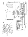
- Fig. 1 shows a module disk MS for a device not otherwise shown here Automation technology.
- the device includes a gateway (not shown here) which among other things the modular panels MS can be stacked.
- the module disc MS is included additional module disks MS can be joined to form a connection block of variable length.
- the module disc MS has a disc-shaped base clamp carrier according to FIG. 1 2 for locking the individual module on a (not shown here) Mounting rail on.
- the basic terminal support 2 is provided with plastic snap-in feet 4 provided with which, in a manner known per se, the latching connection to the mounting rail can be produced.
- the base clamp support 2 comprises a lower base section 6, which is in an area above the mounting rail feet 4 and next to the mounting rail feet 4 extends laterally beyond the mounting rail on both sides.
- the base terminal support 2 perpendicular to its main plane of extent penetrating bus conductor opening 8 for receiving the internal bus conductor section 10 provided that the bus conductor signals are forwarded from individual module to individual module and allowed in the electronic circuit board 14.
- the electronic circuit board 14 is in the area which is approximately from the vertical to the center of the mounting rail to the internal bus conductor section 10 extends, in the base terminal support 2, a peripheral recess 12 educated.
- the electronic circuit board 14 has an electronic circuit (not shown here) for processing / forwarding each to the electronic circuit board 14 provided signals.
- the base section 6 In the area between the internal bus conductor section 10 and the latching foot 4 is the base section 6 with three further openings lying side by side 16, 17, 18 provided, each perpendicular to the main disc or ⁇ module plane Penetrate base terminal support 2 and of which two openings 16, 18 with as preferably designed in one piece cross bridges contact elements 20, 22 ( on one side with a connector pin 20a, 22a, on the other with a matching integrally molded socket 20b, 22b and molded contacts 20c, 22c are provided vertically upward), which pass on the assigned Potentials - preferably of the plus or minus supply potential - of the module to enable module. In their interaction, the contact elements 20, 22 potentials.
- the further opening 17 serves - like further ones not described here Openings in the basic terminal support - only material savings. These potentials are transferred from the cross bridges 20, 22 into the printed circuit board and / or via a suitable separate connector or attached to the electronic circuit board 24 to the connections of the busbars SM, SP in the basic terminal support 2 and led to the connection levels of the module disc MS.
- the recess 12 is at the end of the individual module facing away from the mounting rail bounded by a web 26 projecting perpendicularly from the base section, on its side facing the mounting rail 4 with an insertion groove 28 for insertion the electronic circuit board 14 and an electronics housing 29 is.
- connection section 30 protruding vertically upward from the base section 6 integrally formed with the six arranged in two rows of three individual (A1, A2) and double connections B1, B2, C1, C2 is provided. Openings 34 with a square Cross section next to connection openings 32 for connections A1, A2, B1, B2 ... allow the insertion of a screwdriver to open the in the connection section 30 arranged spring contact elements 36. Outside the third connection level C is in the base section another perpendicular to the module disc plane, the Base terminal support 2 penetrating opening 38 is provided, in which another Contact element 40 is located, through which the protective conductor PE from individual module to individual module is passed on.
- the conductive connection between the contact springs 36 of the connections A, B, C, ... and the electronic circuit board 14 is connected by means of busbars SM (for the negative potential, not recognizable here), SP (for the plus potential), SSI (for the signal) realized, the first of each of the contact springs 36 in the connection area 30 of the base terminal support 2 run vertically down to the base section 6 and then be guided in the base section 6 to the electronic circuit board 14.
- the track SM, SP run from the contact springs 36 in lateral grooves / recesses 42 of the base element 2 is substantially U-shaped on both Main outer surfaces of the base terminal support 2.
- busbars are angled upwards and run to the circumferential recess 12, which in this area with six in two rows side-by-side connection openings 44 for attaching the device plug 24 is provided on the electronic circuit board and / or the edge of the circuit board.
- the end areas of the busbars SSI, SM, SP are designed as stamped and bent part sockets and even form the connection sockets for the connector 24 to the electronic circuit board 14 and / or to the edge of the circuit board.
- a particularly space-saving arrangement of the busbars is achieved that the one of the potential-carrying busbars SM on one outside and the other potential-carrying conductor rail SP on the other outside of the basic terminal support 2 is performed. This takes place only in the area of the connection springs 36 Vias between the two in a connection level B or C side by side lying two double connections B1 and B2 etc.
- a cover housing 46 made of plastic can be placed over the connection section 30, which has openings 48 which are connected to the connection openings 32 and the openings 34 correspond.
- the cover is further provided with a lateral groove 50 which cooperate with the groove 28, the electronic circuit board 14 and the electronic circuit board 14 protective housing 29, which in the plug-in direction SR on the base terminal support 2 is attachable. Support the guide pin on the base terminal support when engaging in an associated opening of the adjacent terminal, the mechanical Connection of the clamp carriers strung together.
- the base terminal support 2 or the module disk MS comprises the following functional areas in the area of the recess 12 on / below the base wall 52 of the recess 12 (viewed from the web 26 inwards towards the mounting rail): - module bus (opening) BUS / 8 - Labeling channel (for one or two signs) 54 - Lateral latching hook 56 as a connection to the neighboring terminal with opening 57 for actuating the latching hook from above 57 - FE contact (functional earth) 58 - Potential guidance contact opening 59 - Sockets / connection openings 44.
- a recess 62 is provided in a particularly space-saving manner for a lower section 64 of a coding element 66 which is removed from the housing 29 of the electronic printed circuit board 14 when the printed circuit board or electronics is placed on it engages in the recess 62 and thus forms the counterpart for an upper coding element section 68 remaining on the electronics unit 12/29.
- the upper and lower coding element sections 64, 68 are provided with adjacent pins 70, 72, see FIG. 2.
- the pins 70, 72 are oriented essentially parallel and / or vertically relative to the main plane (that is, relative to the plane of the drawing in FIG. 2) and only allow the electronics housing 29 to be placed on the base terminal carrier 2 if the elements belong together.
- the electronics housing 29 ( within the meaning of claim 1 first component "of the electrical device) is only in a clearly defined position on the base terminal body 2 ( second component ") can be snapped on.
- the coding element 66 that is, the locking lugs 74 in recesses 76 of the Electronics housing 29 latched upper coding element section 68 together with the the lower coding element section 64 engaging there is guided into the opening 62.
- a rectangular pin 88 attached to the coding element 68 for engagement in an opening 90 of the second coding element ensures that the two coding elements are secured against rotation against each other.
- one with a pin 70, 72 and complementary bushings 71 realized, the interlocking of Pin and socket alone already for this anti-rotation (Fig. 3, 4).
- the pins 70 are designed as half square areas. According to the further variants 3b and 3c, the pins 70 are arranged as sector pieces on the outer circumference of a hexagonal base surface S (FIG. 3b) or octagon base surface A (FIG. 3c), which in the case of various coding variants are circumferentially around 60 ° (hexagon) or 45 ° (octagon) are rotated to each other ( Rotation "). In various, for example also neighboring, variants the pins overlap. In FIG. 3b the pins form a rhombus (120 ° element), alternatively they can be designed as a half hexagon (not shown). In FIG.
- pins 70 are a pentagon (135 ° element) and can also be designed as a half octagon (not shown). With increasing number of corners up to a circle, the number of variants on a base area can be increased in an uncomplicated manner in this way.
- 3d and 4 coding system have the abutting pins 70 and bushings 71 each have essentially a rectangular cross section, which is approximately half Occupies the area of a square area Q of the base plate on which the pegs are aligned according to a coding system in which the pins and bushes 70, 71, 72 of the first and the second coding element each have four different positions ingest, essentially each of the long sides of the rectangle on one of the outer sides of the square area (0.00 a.m., 3.00 a.m., 6.00 a.m., 9 a.m.).
- the base plates 84 of the first and the second coding element section with two and in Fig. 3 with three of the square areas lined up Q to accommodate the rectangular pins and bushings, which makes implement the 16 or 64 coding variants shown in a confined space in a confined space to let.
- FIG. 5 shows an embodiment of the invention in which the two coding element sections 64, 68 of each coding element 66 in one piece via constrictions or Tear-off edges 92 are shaped with a flexible, U-shaped handle 94 with a handle 96 are, which allows easy assembly of the coding element 66 and the danger minimized from confusion during assembly.
- Fig. 5a shows like Fig. 5e the starting position when gripping the handle 94 together with the Coding element sections 64 and 68.
- the flat, band-like handle 94 bend by hand in such a way that the two Snap the coding element sections 64 and 68 together (FIG. 5b).
- the snapped together Coding element 66 directly to a component to be coded (e.g. the housing 29 in Fig. 1) and it is rotated accordingly to Arrow P3 in Fig. 5c, the constriction 92 torn.
- a component to be coded e.g. the housing 29 in Fig. 1
- the constriction 92 torn e.g. the housing 29 in Fig.
- Figure 7 shows a further embodiment of the invention, in which again the two coding element sections 64, 68 of each coding element 66 in one piece Constrictions and tear edges 92 are connected with a flexible handle 94.
- the Handle 96 is formed here as an indentation of the handle 94, which is a special one represents inexpensive implementation of the handle.
- the pins 70 and the bushings 71 are half hexagonal bases trained, which rotate on the circumference of the hexagon in 60 ° steps.
- this variant has proven to be particularly advantageous because the formation of the pins 70 and the bushings 71 as half hexagonal areas is a special one high security against accidental plugging together of not belonging together Coding variants guaranteed. It can also be used in a confined space realize a large number of different coding variants that meet the requirements most of the practical cases.
- the bevels 100 extend laterally beveled edges 82 of the base plate 84 of the second coding element section 64, which when inserting the second coding element section 64 into the recess 62 of the base clamp body 2 snap into the undercut 86, only just over half the width of the base plate 84 and thus just so far that it is still possible, the second coding element section 64 after a lateral displacement on the base terminal support 2 to be pulled vertically upwards (what is possible because the base terminal support 2 as a whole and in particular in this area is somewhat narrower than the entire module disk MS according to the type of FIG. 1 with the covers 29,46).
- the second coding element section can thus 64 can be solved by a consciously executed work step.
- a projection 102 formed on the base plate 84 at the bottom is also included designed, in a correspondingly designed recess (not shown) on the base terminal support 2 engage, so that an accidental sideways shift on the base terminal support 2 is prevented.
- a conscious shift e.g. with help a screwdriver is possible.
Landscapes
- Engineering & Computer Science (AREA)
- Microelectronics & Electronic Packaging (AREA)
- Connector Housings Or Holding Contact Members (AREA)
- Rotary Switch, Piano Key Switch, And Lever Switch (AREA)
- Details Of Resistors (AREA)
- Reduction Or Emphasis Of Bandwidth Of Signals (AREA)
- Electrical Discharge Machining, Electrochemical Machining, And Combined Machining (AREA)
- Compression, Expansion, Code Conversion, And Decoders (AREA)
Priority Applications (1)
| Application Number | Priority Date | Filing Date | Title |
|---|---|---|---|
| EP00115213A EP1119229A1 (fr) | 2000-01-07 | 2000-07-13 | Dispositif électrique codifié |
Applications Claiming Priority (2)
| Application Number | Priority Date | Filing Date | Title |
|---|---|---|---|
| DE19902811 | 1999-01-25 | ||
| DE1999102811 DE19902811C1 (de) | 1999-01-25 | 1999-01-25 | Kodiervorrichtung und Kodierverfahren zur Kodierung eines elektrischen Gerätes |
Publications (3)
| Publication Number | Publication Date |
|---|---|
| EP1052883A2 true EP1052883A2 (fr) | 2000-11-15 |
| EP1052883A3 EP1052883A3 (fr) | 2000-11-22 |
| EP1052883B1 EP1052883B1 (fr) | 2007-03-14 |
Family
ID=7895291
Family Applications (1)
| Application Number | Title | Priority Date | Filing Date |
|---|---|---|---|
| EP00100306A Expired - Lifetime EP1052883B1 (fr) | 1999-01-25 | 2000-01-07 | Dispositif et procédé de codage pour un appareil électrique |
Country Status (5)
| Country | Link |
|---|---|
| US (1) | US6485336B1 (fr) |
| EP (1) | EP1052883B1 (fr) |
| AT (1) | ATE357128T1 (fr) |
| DE (2) | DE19964150A1 (fr) |
| ES (1) | ES2283249T3 (fr) |
Cited By (1)
| Publication number | Priority date | Publication date | Assignee | Title |
|---|---|---|---|---|
| DE102011055920B3 (de) * | 2011-12-01 | 2013-05-29 | Pilz Gmbh & Co. Kg | Separates Zubehörelement für eine Steuerungsvorrichtung |
Families Citing this family (14)
| Publication number | Priority date | Publication date | Assignee | Title |
|---|---|---|---|---|
| US7367121B1 (en) | 2000-01-05 | 2008-05-06 | Protectconnect | Electrical wiring method |
| FR2835391B1 (fr) * | 2002-01-25 | 2004-03-12 | Schneider Automation | Appareil modulaire a detrompage mecanique |
| AU2003248564A1 (en) | 2002-05-23 | 2003-12-12 | Protectconnect, Inc. | Safety module electrical distribution system |
| US7312396B1 (en) | 2004-03-13 | 2007-12-25 | Protectconnect, Inc. | Universal electrical wiring component |
| US7321120B1 (en) | 2004-11-26 | 2008-01-22 | Protectconnect, Inc. | Motion detector module |
| US20080053698A1 (en) | 2006-07-29 | 2008-03-06 | Steve Purves | Pre-wired power distribution system |
| DE202007002248U1 (de) * | 2007-02-15 | 2007-06-06 | Harting Electric Gmbh & Co. Kg | Kodiereinrichtung für Steckverbinder |
| BRPI0818209A2 (pt) * | 2007-10-23 | 2017-06-13 | Abb Ag | borne em série com um conetor |
| US8820359B2 (en) * | 2008-10-21 | 2014-09-02 | The Aerospace Corporation | Seamless fluid storage and transport module |
| DE102008054015B4 (de) * | 2008-10-30 | 2012-11-08 | Lumberg Connect Gmbh | Steckverbinder |
| DE102010041540A1 (de) * | 2010-09-28 | 2012-03-29 | Robert Bosch Gmbh | Steuergerät |
| ES2650040T3 (es) * | 2014-08-27 | 2018-01-16 | Selectron Systems Ag | Disposición con partes modulares y medios de codificación ajustables |
| US10790609B2 (en) * | 2018-10-22 | 2020-09-29 | Honeywell International Inc. | Field termination assembly supporting use of mistake-proof keys |
| DE102019111164A1 (de) * | 2019-04-30 | 2020-11-05 | Wago Verwaltungsgesellschaft Mbh | Steckverbinder einer elektrischen Steckverbindung sowie Set aus Steckverbinder und Funktionselement |
Family Cites Families (14)
| Publication number | Priority date | Publication date | Assignee | Title |
|---|---|---|---|---|
| US3491330A (en) * | 1967-09-22 | 1970-01-20 | Amp Inc | Connector keying system |
| US3984169A (en) * | 1972-03-10 | 1976-10-05 | Harvey Hubbell Incorporated | Keying for lever action connectors |
| US3941447A (en) * | 1974-11-29 | 1976-03-02 | Eastman Kodak Company | Camera flash socket |
| DE7823090U1 (de) * | 1978-08-02 | 1981-07-16 | Standard Elektrik Lorenz Ag, 7000 Stuttgart | Mechanische Codiereinrichtung |
| US4224486A (en) * | 1979-03-05 | 1980-09-23 | Amp Incorporated | Shunt protected power connector |
| JPS5942785A (ja) * | 1982-08-31 | 1984-03-09 | 日本圧着端子製造株式会社 | 電気コネクタ |
| DE8805197U1 (de) * | 1988-04-19 | 1988-06-16 | Siemens AG, 1000 Berlin und 8000 München | Versteifungs- und Kodiervorrichtung |
| DE3830187C3 (de) | 1988-09-06 | 1995-10-26 | Licentia Gmbh | Kodiervorrichtung für Schaltschrankeinschübe |
| US4895535A (en) * | 1989-06-07 | 1990-01-23 | Amp Incorporated | Keyed mountable electrical connectors |
| GB8928879D0 (en) * | 1989-12-21 | 1990-02-28 | Amp Gmbh | Connector keying system |
| DE4121836C2 (de) * | 1991-07-02 | 1994-07-07 | Weidmueller C A Gmbh Co | Reihenklemme mit Aufsteckmodul |
| DE9208701U1 (de) * | 1992-06-29 | 1992-12-17 | Siemens AG, 8000 München | Codiereinrichtung für elektrische Baugruppen |
| DE19710768C2 (de) * | 1997-03-16 | 1999-11-11 | Phoenix Contact Gmbh & Co | Elektrisches oder elektronisches Gerät |
| US6142592A (en) * | 1998-05-19 | 2000-11-07 | Endress & Hauser Gmbh & Co Kg | Instrument system |
-
1999
- 1999-01-25 DE DE19964150A patent/DE19964150A1/de not_active Ceased
-
2000
- 2000-01-07 AT AT00100306T patent/ATE357128T1/de active
- 2000-01-07 ES ES00100306T patent/ES2283249T3/es not_active Expired - Lifetime
- 2000-01-07 EP EP00100306A patent/EP1052883B1/fr not_active Expired - Lifetime
- 2000-01-07 DE DE50014154T patent/DE50014154D1/de not_active Expired - Lifetime
- 2000-01-24 US US09/490,673 patent/US6485336B1/en not_active Expired - Fee Related
Cited By (2)
| Publication number | Priority date | Publication date | Assignee | Title |
|---|---|---|---|---|
| DE102011055920B3 (de) * | 2011-12-01 | 2013-05-29 | Pilz Gmbh & Co. Kg | Separates Zubehörelement für eine Steuerungsvorrichtung |
| EP2600705A2 (fr) | 2011-12-01 | 2013-06-05 | Pilz GmbH & Co. KG | Élément accessoire séparé pour un dispositif de commande |
Also Published As
| Publication number | Publication date |
|---|---|
| EP1052883B1 (fr) | 2007-03-14 |
| DE19964150A1 (de) | 2000-09-07 |
| ES2283249T3 (es) | 2007-11-01 |
| ATE357128T1 (de) | 2007-04-15 |
| DE50014154D1 (de) | 2007-04-26 |
| US6485336B1 (en) | 2002-11-26 |
| EP1052883A3 (fr) | 2000-11-22 |
Similar Documents
| Publication | Publication Date | Title |
|---|---|---|
| EP1022809B1 (fr) | Appareil électrique | |
| DE69601754T2 (de) | Anschlusselement und Klemmverbinder | |
| EP1052883A2 (fr) | Dispositif et procédé de codage pour un appareil électrique | |
| DE3843664C2 (fr) | ||
| DE202017104591U1 (de) | Sockeleinheit für Reiheneinbaugeräteanordnung | |
| EP3490075A1 (fr) | Ensemble composé de connecteur enfichable et d'élément de retenue ainsi que connecteur enfichable et élément de retenue correspondant | |
| DE102023105747A1 (de) | Steckverbinder, Halteelement sowie Set aus einem Steckverbinder und einem Halteelement | |
| EP3981046B1 (fr) | Connecteur de carte de circuit imprimé modulaire | |
| DE2338778B2 (de) | Buchsenleiste | |
| EP0082469B1 (fr) | Boîtier pour loger les composants électriques nécessaires pour l'activation d'une bobine d'un aimant d'une valve hydraulique ou similaire | |
| DE2144768C3 (de) | Anordnung zur Zuordnung bestimmter Einbauplätze für steckbare Flachbaugruppen | |
| DE29906583U1 (de) | Kodiervorrichtung zur Kodierung eines elektrischen Gerätes | |
| EP1052734B1 (fr) | Système de maintien pour des différents types de connecteurs | |
| EP0929135A2 (fr) | Adaptateur multifonction pour des barres d'un système de barres omnibus | |
| DE19514842B4 (de) | Prozeßstecker | |
| EP0655173B1 (fr) | Dispositif pour relier un moteur a au moins deux pistes conductrices | |
| EP0310832A2 (fr) | Support de broches de contact multiples pour des installations basse tension | |
| DE19902811C1 (de) | Kodiervorrichtung und Kodierverfahren zur Kodierung eines elektrischen Gerätes | |
| DE19532623B4 (de) | Elektrischer Stecker mit einem Betätigungsschieber | |
| DE4320539A1 (de) | Leitungsdraht-Verbindungsklemme | |
| EP1085605A2 (fr) | Tronçon de bus pour appareil électrique | |
| EP0295570A2 (fr) | Prise pour connexion d'un appareil téléphonique | |
| EP1003246A2 (fr) | Système de connecteur modulaire | |
| DE4305844C2 (de) | Steckverbinder | |
| CH687677A5 (de) | Bausatz zur Herstellung eines Spielzeugwuerfels. |
Legal Events
| Date | Code | Title | Description |
|---|---|---|---|
| PUAI | Public reference made under article 153(3) epc to a published international application that has entered the european phase |
Free format text: ORIGINAL CODE: 0009012 |
|
| PUAL | Search report despatched |
Free format text: ORIGINAL CODE: 0009013 |
|
| AK | Designated contracting states |
Kind code of ref document: A2 Designated state(s): AT BE CH CY DE DK ES FI FR GB GR IE IT LI LU MC NL PT SE |
|
| AX | Request for extension of the european patent |
Free format text: AL;LT;LV;MK;RO;SI |
|
| AK | Designated contracting states |
Kind code of ref document: A3 Designated state(s): AT BE CH CY DE DK ES FI FR GB GR IE IT LI LU MC NL PT SE |
|
| AX | Request for extension of the european patent |
Free format text: AL;LT;LV;MK;RO;SI |
|
| 17P | Request for examination filed |
Effective date: 20010222 |
|
| AKX | Designation fees paid |
Free format text: AT BE CH CY DE DK ES FI FR GB GR IE IT LI LU MC NL PT SE |
|
| GRAP | Despatch of communication of intention to grant a patent |
Free format text: ORIGINAL CODE: EPIDOSNIGR1 |
|
| GRAS | Grant fee paid |
Free format text: ORIGINAL CODE: EPIDOSNIGR3 |
|
| GRAA | (expected) grant |
Free format text: ORIGINAL CODE: 0009210 |
|
| AK | Designated contracting states |
Kind code of ref document: B1 Designated state(s): AT BE CH CY DE DK ES FI FR GB GR IE IT LI LU MC NL PT SE |
|
| PG25 | Lapsed in a contracting state [announced via postgrant information from national office to epo] |
Ref country code: FI Free format text: LAPSE BECAUSE OF FAILURE TO SUBMIT A TRANSLATION OF THE DESCRIPTION OR TO PAY THE FEE WITHIN THE PRESCRIBED TIME-LIMIT Effective date: 20070314 Ref country code: NL Free format text: LAPSE BECAUSE OF FAILURE TO SUBMIT A TRANSLATION OF THE DESCRIPTION OR TO PAY THE FEE WITHIN THE PRESCRIBED TIME-LIMIT Effective date: 20070314 |
|
| REG | Reference to a national code |
Ref country code: GB Ref legal event code: FG4D Free format text: NOT ENGLISH |
|
| REG | Reference to a national code |
Ref country code: CH Ref legal event code: EP |
|
| REF | Corresponds to: |
Ref document number: 50014154 Country of ref document: DE Date of ref document: 20070426 Kind code of ref document: P |
|
| REG | Reference to a national code |
Ref country code: IE Ref legal event code: FG4D Free format text: LANGUAGE OF EP DOCUMENT: GERMAN |
|
| PG25 | Lapsed in a contracting state [announced via postgrant information from national office to epo] |
Ref country code: SE Free format text: LAPSE BECAUSE OF FAILURE TO SUBMIT A TRANSLATION OF THE DESCRIPTION OR TO PAY THE FEE WITHIN THE PRESCRIBED TIME-LIMIT Effective date: 20070614 |
|
| REG | Reference to a national code |
Ref country code: CH Ref legal event code: NV Representative=s name: ISLER & PEDRAZZINI AG |
|
| PG25 | Lapsed in a contracting state [announced via postgrant information from national office to epo] |
Ref country code: PT Free format text: LAPSE BECAUSE OF FAILURE TO SUBMIT A TRANSLATION OF THE DESCRIPTION OR TO PAY THE FEE WITHIN THE PRESCRIBED TIME-LIMIT Effective date: 20070814 |
|
| NLV1 | Nl: lapsed or annulled due to failure to fulfill the requirements of art. 29p and 29m of the patents act | ||
| ET | Fr: translation filed | ||
| REG | Reference to a national code |
Ref country code: CH Ref legal event code: PCAR Free format text: ISLER & PEDRAZZINI AG;POSTFACH 1772;8027 ZUERICH (CH) |
|
| GBV | Gb: ep patent (uk) treated as always having been void in accordance with gb section 77(7)/1977 [no translation filed] |
Effective date: 20070314 |
|
| REG | Reference to a national code |
Ref country code: ES Ref legal event code: FG2A Ref document number: 2283249 Country of ref document: ES Kind code of ref document: T3 |
|
| PG25 | Lapsed in a contracting state [announced via postgrant information from national office to epo] |
Ref country code: GB Free format text: LAPSE BECAUSE OF FAILURE TO SUBMIT A TRANSLATION OF THE DESCRIPTION OR TO PAY THE FEE WITHIN THE PRESCRIBED TIME-LIMIT Effective date: 20070314 |
|
| REG | Reference to a national code |
Ref country code: IE Ref legal event code: FD4D |
|
| PLBE | No opposition filed within time limit |
Free format text: ORIGINAL CODE: 0009261 |
|
| STAA | Information on the status of an ep patent application or granted ep patent |
Free format text: STATUS: NO OPPOSITION FILED WITHIN TIME LIMIT |
|
| PG25 | Lapsed in a contracting state [announced via postgrant information from national office to epo] |
Ref country code: IE Free format text: LAPSE BECAUSE OF FAILURE TO SUBMIT A TRANSLATION OF THE DESCRIPTION OR TO PAY THE FEE WITHIN THE PRESCRIBED TIME-LIMIT Effective date: 20070314 Ref country code: DK Free format text: LAPSE BECAUSE OF FAILURE TO SUBMIT A TRANSLATION OF THE DESCRIPTION OR TO PAY THE FEE WITHIN THE PRESCRIBED TIME-LIMIT Effective date: 20070314 |
|
| 26N | No opposition filed |
Effective date: 20071217 |
|
| PG25 | Lapsed in a contracting state [announced via postgrant information from national office to epo] |
Ref country code: GR Free format text: LAPSE BECAUSE OF FAILURE TO SUBMIT A TRANSLATION OF THE DESCRIPTION OR TO PAY THE FEE WITHIN THE PRESCRIBED TIME-LIMIT Effective date: 20070615 |
|
| BERE | Be: lapsed |
Owner name: WEIDMULLER INTERFACE G.M.B.H. & CO. Effective date: 20080131 |
|
| PG25 | Lapsed in a contracting state [announced via postgrant information from national office to epo] |
Ref country code: MC Free format text: LAPSE BECAUSE OF NON-PAYMENT OF DUE FEES Effective date: 20080131 |
|
| PG25 | Lapsed in a contracting state [announced via postgrant information from national office to epo] |
Ref country code: BE Free format text: LAPSE BECAUSE OF NON-PAYMENT OF DUE FEES Effective date: 20080131 |
|
| PG25 | Lapsed in a contracting state [announced via postgrant information from national office to epo] |
Ref country code: CY Free format text: LAPSE BECAUSE OF FAILURE TO SUBMIT A TRANSLATION OF THE DESCRIPTION OR TO PAY THE FEE WITHIN THE PRESCRIBED TIME-LIMIT Effective date: 20070314 |
|
| PG25 | Lapsed in a contracting state [announced via postgrant information from national office to epo] |
Ref country code: LU Free format text: LAPSE BECAUSE OF NON-PAYMENT OF DUE FEES Effective date: 20080107 |
|
| PGFP | Annual fee paid to national office [announced via postgrant information from national office to epo] |
Ref country code: AT Payment date: 20130111 Year of fee payment: 14 |
|
| PGFP | Annual fee paid to national office [announced via postgrant information from national office to epo] |
Ref country code: CH Payment date: 20140121 Year of fee payment: 15 |
|
| PGFP | Annual fee paid to national office [announced via postgrant information from national office to epo] |
Ref country code: ES Payment date: 20140129 Year of fee payment: 15 |
|
| REG | Reference to a national code |
Ref country code: AT Ref legal event code: MM01 Ref document number: 357128 Country of ref document: AT Kind code of ref document: T Effective date: 20140107 |
|
| PG25 | Lapsed in a contracting state [announced via postgrant information from national office to epo] |
Ref country code: AT Free format text: LAPSE BECAUSE OF NON-PAYMENT OF DUE FEES Effective date: 20140107 |
|
| REG | Reference to a national code |
Ref country code: CH Ref legal event code: PL |
|
| PG25 | Lapsed in a contracting state [announced via postgrant information from national office to epo] |
Ref country code: CH Free format text: LAPSE BECAUSE OF NON-PAYMENT OF DUE FEES Effective date: 20150131 Ref country code: LI Free format text: LAPSE BECAUSE OF NON-PAYMENT OF DUE FEES Effective date: 20150131 |
|
| REG | Reference to a national code |
Ref country code: FR Ref legal event code: PLFP Year of fee payment: 17 |
|
| REG | Reference to a national code |
Ref country code: ES Ref legal event code: FD2A Effective date: 20160226 |
|
| PG25 | Lapsed in a contracting state [announced via postgrant information from national office to epo] |
Ref country code: ES Free format text: LAPSE BECAUSE OF NON-PAYMENT OF DUE FEES Effective date: 20150108 |
|
| REG | Reference to a national code |
Ref country code: FR Ref legal event code: PLFP Year of fee payment: 18 |
|
| REG | Reference to a national code |
Ref country code: FR Ref legal event code: PLFP Year of fee payment: 19 |
|
| PGFP | Annual fee paid to national office [announced via postgrant information from national office to epo] |
Ref country code: IT Payment date: 20190124 Year of fee payment: 20 Ref country code: DE Payment date: 20190123 Year of fee payment: 20 Ref country code: FR Payment date: 20190123 Year of fee payment: 20 |
|
| REG | Reference to a national code |
Ref country code: DE Ref legal event code: R071 Ref document number: 50014154 Country of ref document: DE |