EP1054346A2 - Carte à puce sans contact comprenant deux feuilles de revêtement - Google Patents
Carte à puce sans contact comprenant deux feuilles de revêtement Download PDFInfo
- Publication number
- EP1054346A2 EP1054346A2 EP00304121A EP00304121A EP1054346A2 EP 1054346 A2 EP1054346 A2 EP 1054346A2 EP 00304121 A EP00304121 A EP 00304121A EP 00304121 A EP00304121 A EP 00304121A EP 1054346 A2 EP1054346 A2 EP 1054346A2
- Authority
- EP
- European Patent Office
- Prior art keywords
- hole
- semiconductor element
- card
- sheet
- core
- Prior art date
- Legal status (The legal status is an assumption and is not a legal conclusion. Google has not performed a legal analysis and makes no representation as to the accuracy of the status listed.)
- Withdrawn
Links
Images


Classifications
-
- G—PHYSICS
- G06—COMPUTING OR CALCULATING; COUNTING
- G06K—GRAPHICAL DATA READING; PRESENTATION OF DATA; RECORD CARRIERS; HANDLING RECORD CARRIERS
- G06K19/00—Record carriers for use with machines and with at least a part designed to carry digital markings
- G06K19/06—Record carriers for use with machines and with at least a part designed to carry digital markings characterised by the kind of the digital marking, e.g. shape, nature, code
- G06K19/067—Record carriers with conductive marks, printed circuits or semiconductor circuit elements, e.g. credit or identity cards also with resonating or responding marks without active components
- G06K19/07—Record carriers with conductive marks, printed circuits or semiconductor circuit elements, e.g. credit or identity cards also with resonating or responding marks without active components with integrated circuit chips
- G06K19/077—Constructional details, e.g. mounting of circuits in the carrier
- G06K19/07749—Constructional details, e.g. mounting of circuits in the carrier the record carrier being capable of non-contact communication, e.g. constructional details of the antenna of a non-contact smart card
- G06K19/0775—Constructional details, e.g. mounting of circuits in the carrier the record carrier being capable of non-contact communication, e.g. constructional details of the antenna of a non-contact smart card arrangements for connecting the integrated circuit to the antenna
-
- G—PHYSICS
- G06—COMPUTING OR CALCULATING; COUNTING
- G06K—GRAPHICAL DATA READING; PRESENTATION OF DATA; RECORD CARRIERS; HANDLING RECORD CARRIERS
- G06K19/00—Record carriers for use with machines and with at least a part designed to carry digital markings
- G06K19/06—Record carriers for use with machines and with at least a part designed to carry digital markings characterised by the kind of the digital marking, e.g. shape, nature, code
- G06K19/067—Record carriers with conductive marks, printed circuits or semiconductor circuit elements, e.g. credit or identity cards also with resonating or responding marks without active components
- G06K19/07—Record carriers with conductive marks, printed circuits or semiconductor circuit elements, e.g. credit or identity cards also with resonating or responding marks without active components with integrated circuit chips
- G06K19/077—Constructional details, e.g. mounting of circuits in the carrier
- G06K19/07749—Constructional details, e.g. mounting of circuits in the carrier the record carrier being capable of non-contact communication, e.g. constructional details of the antenna of a non-contact smart card
- G06K19/07773—Antenna details
- G06K19/07777—Antenna details the antenna being of the inductive type
- G06K19/07779—Antenna details the antenna being of the inductive type the inductive antenna being a coil
- G06K19/07783—Antenna details the antenna being of the inductive type the inductive antenna being a coil the coil being planar
-
- H—ELECTRICITY
- H10—SEMICONDUCTOR DEVICES; ELECTRIC SOLID-STATE DEVICES NOT OTHERWISE PROVIDED FOR
- H10W—GENERIC PACKAGES, INTERCONNECTIONS, CONNECTORS OR OTHER CONSTRUCTIONAL DETAILS OF DEVICES COVERED BY CLASS H10
- H10W72/00—Interconnections or connectors in packages
- H10W72/071—Connecting or disconnecting
- H10W72/072—Connecting or disconnecting of bump connectors
- H10W72/07251—Connecting or disconnecting of bump connectors characterised by changes in properties of the bump connectors during connecting
-
- H—ELECTRICITY
- H10—SEMICONDUCTOR DEVICES; ELECTRIC SOLID-STATE DEVICES NOT OTHERWISE PROVIDED FOR
- H10W—GENERIC PACKAGES, INTERCONNECTIONS, CONNECTORS OR OTHER CONSTRUCTIONAL DETAILS OF DEVICES COVERED BY CLASS H10
- H10W72/00—Interconnections or connectors in packages
- H10W72/20—Bump connectors, e.g. solder bumps or copper pillars; Dummy bumps; Thermal bumps
Definitions
- the present invention relates to a non-contact type IC card composed in such a manner that over-sheets are attached onto the respective faces of a core-sheet to which a semiconductor element and a plane coil are attached.
- the core sheet 52 is made of polyimide resin.
- the plane coil 54 is formed on one face of the core sheet 52.
- the semiconductor element 56 is mounted on one face of the core sheet 52 so that the face of the semiconductor element 56 on which the electrode terminals 58 are formed, that is, the electrode terminal formation face of the semiconductor element 56 can be opposed to one face of the core sheet 52.
- the electrode terminals 58 are electrically connected with the respective terminal sections 54a, 54b (54b is not shown in the drawing) of the plane coil 54.
- over-sheets 62 on one face of each of which an adhesive sheet 60 is formed, are attached onto the respective faces of the core sheet 52. These over-sheets 62 and core sheet 52 are subjected to thermal pressing, so that they are integrally heated, pressed and formed into a single body.
- the core sheet 52 is made of expensive polyimide resin, the unit price of the non-contact type IC card 50 is high.
- the present invention is intended to solve the above problems. Accordingly, it is an object of the present invention to provide a non-contact type IC card which is thin and in which irregularities are seldom caused on the surface of non-contact type IC card.
- a non-contact type IC card comprising: a core sheet made of resin and having first and second surfaces and a through-hole penetrating from the first surface to the second surface; a plane coil formed on the first surface of the core sheet, the plane coil having respective terminals located at a region in the hole; a semiconductor element accommodated in the hole, the semiconductor element having electrodes terminals electrically connected to the respective terminals of the plane coil; and a pair of over sheets, made of resin, for covering the first and second surfaces, respectively, to integrally cover the core sheet with the plane coil and the semiconductor element.
- the semiconductor element is accommodated or housed in the through-hole formed on the core-sheet. Therefore, the thickness of the non-contact type IC card can be reduced, and irregularities are seldom-caused on the surface of the non-contact type IC card.
- the unit price of the product can be lowered.
- the semiconductor element can be mechanically reinforced. Therefore, the mechanical strength of the non-contact type semiconductor element can be enhanced when a bending force or an impact is given to the non-contact type semiconductor element.
- respective terminals can be transversely extending along the first surface of the core sheet over an opening of the hole. Otherwise, respective terminals can be extending into and terminated at the opening region of the hole.
- a thickness of the semiconductor element may be substantially the same or a little smaller than that of the core sheet, so that the semiconductor element can thus be accommodated in the hole within a range of thickness of the core sheet.
- the core sheet 12 is made of resin material, and the through-hole 14 is formed in the core sheet 12 so as to penetrate from the upper surface to the lower surface of the IC card.
- the core sheet 12 is made of polyethylene resin, such as PET, which is less expensive than polyimide resin, the manufacturing cost of the non-contact type IC card 10 can be preferably reduced.
- the plane coil 54 is formed on one face of the core sheet 12, that is, the plane coil 54 is formed on a lower face of the core sheet 12 as shown in Fig. 4.
- the plane coil 54 is made of metal such as aluminum or copper, and both terminal sections 54a, 54b of the plane coil 54 are arranged in the through-hole 14.
- the terminal sections 54a, 54b of the plane coil 54 are arranged over the through-hole 14, and at least portions of the terminal sections 54a, 54b with which the electrode terminals 58 of the semiconductor element 56 are connected are plated with gold.
- the semiconductor element 56 is housed in the through-hole 14 from the other face side (the upper face side shown in Fig. 4) of the core sheet 12 so that the face on which the electrode terminals 58 are formed, that is, the electrode terminal formation face can be directed onto the plane coil 54 side, and a pair of electrode terminals 58 are electrically connected with the terminal sections 54a, 54b of the plane coil 54 by means of ultrasonic bonding.
- the semiconductor element 56 when a thin semiconductor element 56, the thickness of which is approximately 50 ⁇ , is used, the semiconductor element 56 does not protrude from the surface of the commonly used core sheet 12 made of PET, the thickness of which is approximately 75 ⁇ . Therefore, no protruding portion are formed on the surface of the non-contact type IC card 10. Further the thickness of the non-contact type IC card 10 can be reduced. In this connection, in order to prevent the occurrence of irregularities, it is preferable that the thickness of the core sheet 12 and that of the semiconductor element 56 (the thickness of the semiconductor element 56 including the electrode terminals 58) are made equal to each other.
- These over-sheets 62 are integrated with the core sheet 12 when they are heated and pressed by means of thermal press.
- the over-sheets 62 are made of polyethylene resin which is less expensive than polyimide resin.
- the through-hole 14 is formed on the core sheet 12 as shown in Fig. 1.
- the profile and size of the through-hole 14 are determined so that the semiconductor element 56 can be housed in the through-hole 14 while consideration is given to the profile of the semiconductor element 56.
- the thickness of the core sheet 12 is determined by giving consideration to the thickness of the semiconductor element 56, that is, it is preferable that the thickness of the core sheet 12 is the same as the thickness of the semiconductor element 56.
- a layer of foil 16 of metal such as copper or aluminum is made to adhere onto one face of the core sheet 12, that is, a layer of foil 16 of metal such as copper or aluminum is made to adhere onto a lower face shown in Fig. 1 as illustrated in Fig. 2.
- the layer of metallic foil 16 is etched in a predetermined pattern, so that the plane coil 54 is formed on one face of the core sheet 12.
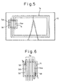
- An example of the plan profile of the plane coil 54 is shown in Fig. 5.
- the plane coil 54 is arranged so that a portion of the plane coil 54 can be arranged over the through-hole 14.
- the terminal sections 54a, 54b are also arranged over the through-hole 14.
- the terminal sections 54a, 54b may be plated with gold.
- the semiconductor element 56 is housed in the through-hole 14 in such a manner that the electrode terminal forming face is directed to the plane coil 54 side as shown in Fig. 3.
- the semiconductor element 56 is housed in the through-hole 14 while the semiconductor element 56 is being positioned so that a pair of electrode terminals 58 formed on the electrode terminal face can be contacted with the terminal sections 54a, 54b of the plane coil 54.
- the electrode terminals 58 of the semiconductor element 56 are electrically connected with the terminal sections 54a, 54b of the plane coil 54 by means of ultrasonic bonding.
- These over-sheets 62 are integrated with both faces of the core sheet 12 when they are heated and pressed by means of thermal press as shown in Fig. 4. In this way, the non-contact type IC card illustrated in Fig. 4 can be manufactured.
Landscapes
- Engineering & Computer Science (AREA)
- Microelectronics & Electronic Packaging (AREA)
- Physics & Mathematics (AREA)
- General Physics & Mathematics (AREA)
- Theoretical Computer Science (AREA)
- Computer Hardware Design (AREA)
- Computer Networks & Wireless Communication (AREA)
- Credit Cards Or The Like (AREA)
Applications Claiming Priority (2)
| Application Number | Priority Date | Filing Date | Title |
|---|---|---|---|
| JP14177299A JP3517374B2 (ja) | 1999-05-21 | 1999-05-21 | 非接触型icカードの製造方法 |
| JP14177299 | 1999-05-21 |
Publications (2)
| Publication Number | Publication Date |
|---|---|
| EP1054346A2 true EP1054346A2 (fr) | 2000-11-22 |
| EP1054346A3 EP1054346A3 (fr) | 2001-09-12 |
Family
ID=15299827
Family Applications (1)
| Application Number | Title | Priority Date | Filing Date |
|---|---|---|---|
| EP00304121A Withdrawn EP1054346A3 (fr) | 1999-05-21 | 2000-05-16 | Carte à puce sans contact comprenant deux feuilles de revêtement |
Country Status (4)
| Country | Link |
|---|---|
| US (2) | US20020030255A1 (fr) |
| EP (1) | EP1054346A3 (fr) |
| JP (1) | JP3517374B2 (fr) |
| KR (1) | KR20010014925A (fr) |
Cited By (4)
| Publication number | Priority date | Publication date | Assignee | Title |
|---|---|---|---|---|
| EP1302894A3 (fr) * | 2001-10-12 | 2003-10-29 | Multitape GmbH | Carte à puce sans contacts et procédure de fabrication |
| WO2009004139A3 (fr) * | 2007-05-21 | 2009-02-19 | Fasver | Vignette adhesive souple de securite dotee d'au moins un microcircuit sans contact pour document officiel |
| WO2013152840A1 (fr) * | 2012-04-10 | 2013-10-17 | Smartrac Ip B.V. | Couche transpondeur et procédé de fabrication de ladite couche |
| CN103366215A (zh) * | 2012-04-05 | 2013-10-23 | 英飞凌科技股份有限公司 | 用于无接触数据传输的数据载体及其产生方法 |
Families Citing this family (6)
| Publication number | Priority date | Publication date | Assignee | Title |
|---|---|---|---|---|
| JP2003044818A (ja) * | 2001-07-31 | 2003-02-14 | Toppan Forms Co Ltd | コンビネーション型icカードの製造方法 |
| KR20040024696A (ko) * | 2002-09-16 | 2004-03-22 | 위영환 | 내장형 무선안테나를 피이티 시트에 형성하는 방법,피이티 시트를 이용한 스마트카드 제조방법 및 상기방법에 의하여 제조된 스마트카드 |
| JP3866178B2 (ja) * | 2002-10-08 | 2007-01-10 | 株式会社ルネサステクノロジ | Icカード |
| JP2004185208A (ja) * | 2002-12-02 | 2004-07-02 | Sony Corp | Icカード |
| JP4479209B2 (ja) * | 2003-10-10 | 2010-06-09 | パナソニック株式会社 | 電子回路装置およびその製造方法並びに電子回路装置の製造装置 |
| US7259678B2 (en) * | 2003-12-08 | 2007-08-21 | 3M Innovative Properties Company | Durable radio frequency identification label and methods of manufacturing the same |
Family Cites Families (16)
| Publication number | Priority date | Publication date | Assignee | Title |
|---|---|---|---|---|
| JPS61201390A (ja) * | 1985-03-04 | 1986-09-06 | Casio Comput Co Ltd | Icカ−ド |
| JPH074995B2 (ja) * | 1986-05-20 | 1995-01-25 | 株式会社東芝 | Icカ−ド及びその製造方法 |
| US5480842A (en) * | 1994-04-11 | 1996-01-02 | At&T Corp. | Method for fabricating thin, strong, and flexible die for smart cards |
| DE4431605C2 (de) * | 1994-09-05 | 1998-06-04 | Siemens Ag | Verfahren zur Herstellung eines Chipkartenmoduls für kontaktlose Chipkarten |
| US5528222A (en) * | 1994-09-09 | 1996-06-18 | International Business Machines Corporation | Radio frequency circuit and memory in thin flexible package |
| US5952713A (en) * | 1994-12-27 | 1999-09-14 | Takahira; Kenichi | Non-contact type IC card |
| JP4015717B2 (ja) * | 1995-06-29 | 2007-11-28 | 日立マクセル株式会社 | 情報担体の製造方法 |
| US5786626A (en) * | 1996-03-25 | 1998-07-28 | Ibm Corporation | Thin radio frequency transponder with leadframe antenna structure |
| FR2760113B1 (fr) * | 1997-02-24 | 1999-06-04 | Gemplus Card Int | Procede de fabrication de carte sans contact a antenne bobinee |
| JPH10242333A (ja) * | 1997-03-01 | 1998-09-11 | Nitto Denko Corp | 半導体装置及び半導体装置の製造方法 |
| KR100330652B1 (ko) * | 1997-06-23 | 2002-03-29 | 사토 게니치로 | Ic모듈 및 ic카드 |
| JPH1134562A (ja) * | 1997-07-17 | 1999-02-09 | Tokin Corp | 非接触カード |
| FR2769441A1 (fr) * | 1997-10-07 | 1999-04-09 | Philips Electronics Nv | Carte electronique sans contact et son procede de fabrication |
| KR100293419B1 (ko) * | 1998-08-10 | 2001-09-17 | 김양성 | 접촉또는비접촉겸용아이씨카드및그제조방법 |
| KR100284111B1 (ko) * | 1998-11-07 | 2001-08-07 | 주동욱 | 전도성접착필름을 사용한 비접촉식아이씨카드와 그 제조방법 |
| KR100284112B1 (ko) * | 1998-11-07 | 2001-08-07 | 주동욱 | 카드의 두께를 줄인 비접촉식아이씨카드와 그 제조방법 |
-
1999
- 1999-05-21 JP JP14177299A patent/JP3517374B2/ja not_active Expired - Fee Related
-
2000
- 2000-05-16 EP EP00304121A patent/EP1054346A3/fr not_active Withdrawn
- 2000-05-18 US US09/573,505 patent/US20020030255A1/en not_active Abandoned
- 2000-05-18 KR KR1020000026606A patent/KR20010014925A/ko not_active Ceased
-
2002
- 2002-11-01 US US10/285,624 patent/US20030057536A1/en not_active Abandoned
Non-Patent Citations (1)
| Title |
|---|
| None * |
Cited By (6)
| Publication number | Priority date | Publication date | Assignee | Title |
|---|---|---|---|---|
| EP1302894A3 (fr) * | 2001-10-12 | 2003-10-29 | Multitape GmbH | Carte à puce sans contacts et procédure de fabrication |
| WO2009004139A3 (fr) * | 2007-05-21 | 2009-02-19 | Fasver | Vignette adhesive souple de securite dotee d'au moins un microcircuit sans contact pour document officiel |
| CN103366215A (zh) * | 2012-04-05 | 2013-10-23 | 英飞凌科技股份有限公司 | 用于无接触数据传输的数据载体及其产生方法 |
| CN103366215B (zh) * | 2012-04-05 | 2016-08-03 | 英飞凌科技股份有限公司 | 用于无接触数据传输的数据载体及其产生方法 |
| WO2013152840A1 (fr) * | 2012-04-10 | 2013-10-17 | Smartrac Ip B.V. | Couche transpondeur et procédé de fabrication de ladite couche |
| US9792543B2 (en) | 2012-04-10 | 2017-10-17 | Smartrac I.P. B.V. | Transponder layer and method for the production thereof |
Also Published As
| Publication number | Publication date |
|---|---|
| EP1054346A3 (fr) | 2001-09-12 |
| US20020030255A1 (en) | 2002-03-14 |
| KR20010014925A (ko) | 2001-02-26 |
| JP3517374B2 (ja) | 2004-04-12 |
| JP2000331138A (ja) | 2000-11-30 |
| US20030057536A1 (en) | 2003-03-27 |
Similar Documents
| Publication | Publication Date | Title |
|---|---|---|
| EP1514698B1 (fr) | Carte à puce et module à puce | |
| US6435415B1 (en) | Contactless electronic memory card | |
| EP0854511B1 (fr) | Dispositif semi-conducteur du type à encapsulation par résine | |
| JPH054483A (ja) | Icチツプを具えた識別カードの製造方法 | |
| EP1065627A2 (fr) | Carte à puce sans contact et procédé de fabrication | |
| US20120201994A1 (en) | Functional laminate | |
| JP2000182017A (ja) | 接触型非接触型共用icカードおよびその製造方法 | |
| CN100359682C (zh) | 电子标签及其制造方法 | |
| EP1054346A2 (fr) | Carte à puce sans contact comprenant deux feuilles de revêtement | |
| KR20000069487A (ko) | 칩카드내에 장치하기 위한 반도체 칩용 캐리어 소자 | |
| EP0886239B1 (fr) | Module sans fil et carte sans fil | |
| US6255725B1 (en) | IC card and plane coil for IC card | |
| JP2844085B2 (ja) | 回路基板及び半導体素子の実装方法 | |
| US20040256150A1 (en) | Nonconducting substrate, forming a strip or a panel, on which a multiplicity of carrier elements are formed | |
| EP4453786A1 (fr) | Cartes à puce dotées de couches métalliques | |
| US6374486B1 (en) | Smart card and process for manufacturing the same | |
| AU2006252092B2 (en) | Card and manufacturing method | |
| KR101158128B1 (ko) | 기판 상에 전자 부품을 장착하는 방법 | |
| CN1264480A (zh) | 制造无接触灵巧卡的方法 | |
| EP1001364B1 (fr) | Carte a circuit integre et bobine plate pour une telle carte | |
| JP3382487B2 (ja) | 非接触icカードおよびその製造方法 | |
| JP2001203296A (ja) | Icカード用icチップ実装基板 | |
| KR20220013204A (ko) | 메탈 카드 및 그 제조 방법 | |
| US20250045555A1 (en) | Method for producing a smart card inlay, smart card inlay and smart card | |
| JP3764213B2 (ja) | Icカード及びその製造方法 |
Legal Events
| Date | Code | Title | Description |
|---|---|---|---|
| PUAI | Public reference made under article 153(3) epc to a published international application that has entered the european phase |
Free format text: ORIGINAL CODE: 0009012 |
|
| AK | Designated contracting states |
Kind code of ref document: A2 Designated state(s): AT BE CH CY DE DK ES FI FR GB GR IE IT LI LU MC NL PT SE Kind code of ref document: A2 Designated state(s): DE FR GB |
|
| AX | Request for extension of the european patent |
Free format text: AL;LT;LV;MK;RO;SI |
|
| PUAL | Search report despatched |
Free format text: ORIGINAL CODE: 0009013 |
|
| AK | Designated contracting states |
Kind code of ref document: A3 Designated state(s): AT BE CH CY DE DK ES FI FR GB GR IE IT LI LU MC NL PT SE |
|
| AX | Request for extension of the european patent |
Free format text: AL;LT;LV;MK;RO;SI |
|
| 17P | Request for examination filed |
Effective date: 20020215 |
|
| AKX | Designation fees paid |
Free format text: DE FR GB |
|
| 17Q | First examination report despatched |
Effective date: 20061019 |
|
| STAA | Information on the status of an ep patent application or granted ep patent |
Free format text: STATUS: THE APPLICATION IS DEEMED TO BE WITHDRAWN |
|
| 18D | Application deemed to be withdrawn |
Effective date: 20070301 |