EP1065627A2 - Carte à puce sans contact et procédé de fabrication - Google Patents
Carte à puce sans contact et procédé de fabrication Download PDFInfo
- Publication number
- EP1065627A2 EP1065627A2 EP00305371A EP00305371A EP1065627A2 EP 1065627 A2 EP1065627 A2 EP 1065627A2 EP 00305371 A EP00305371 A EP 00305371A EP 00305371 A EP00305371 A EP 00305371A EP 1065627 A2 EP1065627 A2 EP 1065627A2
- Authority
- EP
- European Patent Office
- Prior art keywords
- semiconductor element
- plane coil
- electrode terminals
- terminal sections
- insulating resin
- Prior art date
- Legal status (The legal status is an assumption and is not a legal conclusion. Google has not performed a legal analysis and makes no representation as to the accuracy of the status listed.)
- Withdrawn
Links
Images


Classifications
-
- G—PHYSICS
- G06—COMPUTING OR CALCULATING; COUNTING
- G06K—GRAPHICAL DATA READING; PRESENTATION OF DATA; RECORD CARRIERS; HANDLING RECORD CARRIERS
- G06K19/00—Record carriers for use with machines and with at least a part designed to carry digital markings
- G06K19/06—Record carriers for use with machines and with at least a part designed to carry digital markings characterised by the kind of the digital marking, e.g. shape, nature, code
- G06K19/067—Record carriers with conductive marks, printed circuits or semiconductor circuit elements, e.g. credit or identity cards also with resonating or responding marks without active components
-
- G—PHYSICS
- G06—COMPUTING OR CALCULATING; COUNTING
- G06K—GRAPHICAL DATA READING; PRESENTATION OF DATA; RECORD CARRIERS; HANDLING RECORD CARRIERS
- G06K19/00—Record carriers for use with machines and with at least a part designed to carry digital markings
- G06K19/06—Record carriers for use with machines and with at least a part designed to carry digital markings characterised by the kind of the digital marking, e.g. shape, nature, code
- G06K19/067—Record carriers with conductive marks, printed circuits or semiconductor circuit elements, e.g. credit or identity cards also with resonating or responding marks without active components
- G06K19/07—Record carriers with conductive marks, printed circuits or semiconductor circuit elements, e.g. credit or identity cards also with resonating or responding marks without active components with integrated circuit chips
- G06K19/077—Constructional details, e.g. mounting of circuits in the carrier
- G06K19/07749—Constructional details, e.g. mounting of circuits in the carrier the record carrier being capable of non-contact communication, e.g. constructional details of the antenna of a non-contact smart card
- G06K19/0775—Constructional details, e.g. mounting of circuits in the carrier the record carrier being capable of non-contact communication, e.g. constructional details of the antenna of a non-contact smart card arrangements for connecting the integrated circuit to the antenna
-
- G—PHYSICS
- G06—COMPUTING OR CALCULATING; COUNTING
- G06K—GRAPHICAL DATA READING; PRESENTATION OF DATA; RECORD CARRIERS; HANDLING RECORD CARRIERS
- G06K19/00—Record carriers for use with machines and with at least a part designed to carry digital markings
- G06K19/06—Record carriers for use with machines and with at least a part designed to carry digital markings characterised by the kind of the digital marking, e.g. shape, nature, code
- G06K19/067—Record carriers with conductive marks, printed circuits or semiconductor circuit elements, e.g. credit or identity cards also with resonating or responding marks without active components
- G06K19/07—Record carriers with conductive marks, printed circuits or semiconductor circuit elements, e.g. credit or identity cards also with resonating or responding marks without active components with integrated circuit chips
- G06K19/077—Constructional details, e.g. mounting of circuits in the carrier
- G06K19/07749—Constructional details, e.g. mounting of circuits in the carrier the record carrier being capable of non-contact communication, e.g. constructional details of the antenna of a non-contact smart card
-
- H—ELECTRICITY
- H10—SEMICONDUCTOR DEVICES; ELECTRIC SOLID-STATE DEVICES NOT OTHERWISE PROVIDED FOR
- H10W—GENERIC PACKAGES, INTERCONNECTIONS, CONNECTORS OR OTHER CONSTRUCTIONAL DETAILS OF DEVICES COVERED BY CLASS H10
- H10W72/00—Interconnections or connectors in packages
- H10W72/071—Connecting or disconnecting
- H10W72/072—Connecting or disconnecting of bump connectors
-
- H—ELECTRICITY
- H10—SEMICONDUCTOR DEVICES; ELECTRIC SOLID-STATE DEVICES NOT OTHERWISE PROVIDED FOR
- H10W—GENERIC PACKAGES, INTERCONNECTIONS, CONNECTORS OR OTHER CONSTRUCTIONAL DETAILS OF DEVICES COVERED BY CLASS H10
- H10W72/00—Interconnections or connectors in packages
- H10W72/90—Bond pads, in general
-
- H—ELECTRICITY
- H10—SEMICONDUCTOR DEVICES; ELECTRIC SOLID-STATE DEVICES NOT OTHERWISE PROVIDED FOR
- H10W—GENERIC PACKAGES, INTERCONNECTIONS, CONNECTORS OR OTHER CONSTRUCTIONAL DETAILS OF DEVICES COVERED BY CLASS H10
- H10W72/00—Interconnections or connectors in packages
- H10W72/90—Bond pads, in general
- H10W72/941—Dispositions of bond pads
- H10W72/9415—Dispositions of bond pads relative to the surface, e.g. recessed, protruding
-
- H—ELECTRICITY
- H10—SEMICONDUCTOR DEVICES; ELECTRIC SOLID-STATE DEVICES NOT OTHERWISE PROVIDED FOR
- H10W—GENERIC PACKAGES, INTERCONNECTIONS, CONNECTORS OR OTHER CONSTRUCTIONAL DETAILS OF DEVICES COVERED BY CLASS H10
- H10W72/00—Interconnections or connectors in packages
- H10W72/90—Bond pads, in general
- H10W72/951—Materials of bond pads
- H10W72/952—Materials of bond pads comprising metals or metalloids, e.g. PbSn, Ag or Cu
-
- H—ELECTRICITY
- H10—SEMICONDUCTOR DEVICES; ELECTRIC SOLID-STATE DEVICES NOT OTHERWISE PROVIDED FOR
- H10W—GENERIC PACKAGES, INTERCONNECTIONS, CONNECTORS OR OTHER CONSTRUCTIONAL DETAILS OF DEVICES COVERED BY CLASS H10
- H10W90/00—Package configurations
- H10W90/701—Package configurations characterised by the relative positions of pads or connectors relative to package parts
- H10W90/721—Package configurations characterised by the relative positions of pads or connectors relative to package parts of bump connectors
- H10W90/724—Package configurations characterised by the relative positions of pads or connectors relative to package parts of bump connectors between a chip and a stacked insulating package substrate, interposer or RDL
Definitions
- the present invention relates to a non-contact type IC card including a plane coil and a semiconductor element arranged at a position not overlapping with the plane coil, wherein the terminal sections of the plane coil are electrically connected with the electrode terminals of the semiconductor element. Further, the present invention relates to a process for manufacturing the non-contact type IC card. Furthermore, the present invention relates to the plane coil used for the non-contact type IC card.
- the plane coil 52 is manufactured by winding a covered conductor wire, etching a layer of metallic foil formed on a resin film or punching a metallic sheet.
- the semiconductor element 54 is arranged in the substantially same plane as that of the plane coil 52 at a position not overlapping with the plane coil 52.
- the electrode terminals 56 of the semiconductor element 54 are electrically connected with the terminal sections 52a of the plane coil 52 by wires 58.
- bonding wires and covered wires are included in the implications of the "wires" in this specification hereinafter.
- a pair of over-sheets 60 made of resin are attached onto both sides of the plane coil 52 and semiconductor element 54.
- the over-sheets 60 are heated and pressed, so that they can be integrated into one body.
- the non-contact type IC card 50 can be made.
- insulating material such as an insulating sheet is interposed between the wires 58 and the plane coil 52 so that an electrical insulating property can be ensured.
- the thickness of the non-contact type IC card 50 is reduced by arranging the plane coil 52 and the semiconductor element 54 in such a manner that they are not overlapped with each other.
- the thickness of the plane coil 52 itself and that of the semiconductor element 54 itself must be further reduced.
- the present invention has been accomplished to solve the above problems. It is an object of the present invention to provide a non-contact type IC card, the thickness of which is small, which is less susceptible to damage.
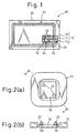
- an IC card comprising: a plane coil having respective terminal sections; a semiconductor element arranged at a position not overlapping with the plane coil, the semiconductor element having electrode terminals; means for electrically connecting the respective terminal sections of the plane coil to the electrode terminals of the semiconductor element; and a reinforcing frame arranged on a same face as that of the semiconductor element so that the semiconductor element is surrounded by the reinforcing frame.
- the semiconductor element is arranged inside the reinforcing frame. In other words, the semiconductor element is surrounded by the reinforcing frame. Therefore, the semiconductor element is protected when an external force is given to the semiconductor element. Accordingly, even if the thickness of the semiconductor element is reduced, no problems are caused, that is, there is no possibility that the semiconductor element is damaged.
- the reinforcing frame is composed in such a manner that the terminal sections of the plane coil are formed into a frame-shape, it becomes unnecessary to provide the reinforcing frame separately from the plane coil. Therefore, the number of parts can be reduced.
- the inside region of the reinforcing frame is filled with resin material by using the reinforcing frame as a guide, the semiconductor element can be protected by the resin, so that the possibility of damage of the semiconductor element can be reduced.
- the semiconductor element is arranged inside the plane coil, the dimensions of the non-contact type IC card can be reduced, which is advantageous for use in various technical fields in which small non-contact type IC cards are required.
- the reinforcing frame comprises the respective terminal sections which constituted a frame-like configuration.
- An inside region of the reinforcing frame is filled with a resin.
- the semiconductor element is arranged at a position inside the plane coil.
- the electrical connecting means comprises a circuit board extending from the terminal sections of the plane coil to the electrode terminals of the semiconductor element, the circuit board comprising an insulating resin film having first and second surfaces, the first surface facing to the semiconductor element, and circuit patterns formed on the second surface of the insulating resin film; and conductive bumps formed on the terminal sections of the plane coil and on the electrode terminals of the semiconductor element, respectively, the bumps projecting through the insulating resin film to the circuit patterns, so that the terminal sections of the plane coil are electrically connected to the electrode terminals of the semiconductor element by means of the circuit patterns.
- the electrical connecting means comprises: an insulating resin film extending from the terminal sections of the plane coil to the electrode terminals of the semiconductor element, the insulating resin film having first and second surfaces, the first surface facing to the semiconductor element, the insulating resin film also having through holes at positions corresponding to the terminal sections of the plane coil and the electrode terminals of the semiconductor element; and circuit patterns, composed of conductive paste, formed on the second surface of the insulating resin film and having respective ends filled in the through holes, respectively, so that the terminal sections of the plane coil are electrically connected to the electrode terminals of the semiconductor element by means of the circuit patterns.
- an IC card further comprises an electrically insulating layer for covering the reinforcing frame, the semiconductor element and the plane coil, at a side of the electrode terminals of the semiconductor element; the electrical connecting means comprising:
- the electrical connecting means comprises: an insulating resin thin film extending from the terminal sections of the plane coil to the electrode terminals of the semiconductor element, the insulating resin film having first and second surfaces, the first surface facing the semiconductor element; the insulating resin film having relief portions at positions corresponding to the terminal sections of the plane coil and the electrode terminals of the semiconductor element; circuit patterns, composed of conductive metal foil, formed on the second surface of the insulating resin film and having respective portions pushed toward the terminal sections of the plane coil and the electrode terminals of the semiconductor element through the relief portions of the insulating resin film, so that the terminal sections of the plane coil are electrically connected to the electrode terminals of the semiconductor element by means of the circuit patterns.
- a process for manufacturing a non-contact type IC card comprising the following steps of:
- Another process for manufacturing a non-contact type IC card comprises the following steps of:
- Still another process for manufacturing a non-contact type IC card comprises the following steps of:
- a further process for manufacturing a non-contact type IC card comprises the following steps of:
- a plane coil adapted to be used in a non-contact type IC card including at least one semiconductor element, the plane coil comprising: respective terminal sections, at least one of the terminal sections being formed as a reinforcing frame, so that the semiconductor element can be arranged in such a manner that the semiconductor element is surrounded by the reinforcing frame.
- the plane coil 52 can be manufactured by various manufacturing processes, the plane coil 52 manufactured by punching or etching a thin metallic sheet is preferable for the non-contact type IC card 10 of the present invention.
- the thickness of the semiconductor element 54 is reduced, and the semiconductor element 54 is arranged on substantially the same face as that of the plane coil 52 at a position where the semiconductor element 54 does not overlap with the plane coil 52.
- the thickness of the semiconductor element 54 is approximately 30 to 50 ⁇ m.
- the semiconductor element 54 is arranged close to the plane coil 52 in the inside region of the plane coil 52. However, it is also possible to arrange the semiconductor element 54 in the outside region of the plane coil 52.
- the semiconductor element 54 is arranged inside the reinforcing frame 12 arranged on the same face as that of the semiconductor element 54.
- the reinforcing frame 12 is arranged in the periphery of the semiconductor element 54.
- the thickness 12 of the reinforcing frame 12 is substantially the same as the thickness of the semiconductor element 54 or is somewhat larger than the thickness of the semiconductor element 54.
- the reinforcing frame 12 is made of, for example, a thin metallic sheet, a thin ceramic sheet or a rigid resin material.
- the profile of the inner circumferential face of the reinforcing frame 12 is somewhat larger than the outer profile of the semiconductor element 54, so that a large gap can not be formed between the inner circumferential face of the reinforcing frame 12 and the outer edge of the semiconductor element 54.
- the wiring board 18 composed of the insulating resin film body 16, one side of which is directed to the semiconductor element 54 side, on the other side of which two wiring patterns 14 are formed, is arranged between the terminal sections 52a of the plane coil 52 and the electrode terminals 56 of the semiconductor element 54 on the electrode terminal 56 side of the semiconductor element 54.
- the bumps 20, 22 protruding to the wiring board 18 side are respectively formed in the terminal sections 52a of the plane coil 52 and the electrode terminals 56 of the semiconductor element 54.
- a pair of over-sheets 60, on one side of which the adhesive layer 60a is formed, are attached onto both sides of the plane coil 52, semiconductor element 54 and wiring board 18 in such a manner that the adhesive layers 60a of the over-sheets 60 are directed to the plane coil 52 side. Then, the over-sheets 60 are heated and pressed so that they can be integrated into one body. As shown in Fig. 3, when the over-sheets 60 are heated and pressed in this way, a tip portion of each bump 20, 22 penetrates the insulating resin film body 16 of the wiring board 18 and comes into electrical contact with the wiring pattern 14. Due to the foregoing, the terminal sections 52a of the plane coil 52 and the electrode terminals 56 of the semiconductor element 54 are electrically connected with each other.
- this non-contact type IC card 10 is described as follows. First, when the plane coil 52 and the semiconductor element 54 are manufactured, the bumps 20, 22 protruding outward are respectively formed in the terminal sections 52a of the plane coil 52 and electrode terminals 56 of the semiconductor element 54.
- the reinforcing frame 12 is arranged in the periphery of the semiconductor element 54.
- the semiconductor element 54 is arranged at a position not overlapping with the plane coil 52 in the substantially same plane as that of the plane coil 52.
- the reinforcing frame 12 is arranged in the periphery of the semiconductor element 54 in the same plane as that of the semiconductor element 54.
- the reinforcing frame 12 may be arranged in the substantially same plane as that of the plane coil 52 at a position not overlapping with the plane coil 52, and the semiconductor element 54 may be arranged inside the reinforcing frame 12 in the same plane as that of the reinforcing frame 12.
- the wiring board 18 is arranged on the electrode terminal 56 side of the semiconductor element 54 while the other side of the wiring board 18 is directed to the semiconductor element 54 side in such a manner that the wiring board 18 is set between the terminal sections 52a of the plane coil 52 and the electrode terminals 56 of the semiconductor element 54.
- a pair of over-sheets 60 on one side of which the adhesive layer 60a is formed, are attached to the plane coil 52, semiconductor element 54 and wiring board 18 in such a manner that each adhesive layer 60a is directed onto the plane coil 52 side. Then, the pair of over-sheets 60 are heated and pressed so that they can be integrated into one body. Due to the foregoing, the plane coil 52, semiconductor element 54, reinforcing frame 12 and wiring board 18, which are interposed between the pair of over-sheets 60, are integrated into one body. When the wiring board 18 is pressed and heated, the bumps 22 penetrate the insulating resin film 16, and their tips come into electrical contact with the wiring pattern 14.
- the portions of the insulating resin film 16 corresponding to the positions of the bumps 20, 22 are beforehand removed to form through holes, so that the wiring pattern 14 is exposed at the bottom surface of these through holes. Due to the foregoing, the terminal sections 52a of the plane coil 52 and the electrode terminals 56 of the semiconductor element 54 are electrically connected with each other by the wiring pattern 14.
- This embodiment is the same as the first embodiment, except for the electrical connection structure of the terminal sections 52a of the plane coil 52 with the electrode terminals 56 of the semiconductor element 54 of the non-contact type IC card, as will be explained with reference to Figs. 5 and 6.
- the reinforcing frame 12 is arranged in the periphery of the semiconductor element 54. Specifically, first, the semiconductor element 54 is arranged at a position not overlapping with the plane coil 52 in substantially the same plane as that of the plane coil 52. After that, the reinforcing frame 12 is arranged so that the semiconductor element 54 can be located inside, that is, the semiconductor element 54 can be surrounded. As described in the first embodiment, the reinforcing frame 12 may be arranged in the substantially same plane as that of the plane coil 52 at a position not overlapping with the plane coil 52, and the semiconductor element 54 may be arranged inside the reinforcing frame 12 in the same plane as that of the reinforcing frame 12.
- the insulating resin film 16, on which the through-holes 24 are formed at positions corresponding to the terminal sections 52a of the plane coil 52 and the electrode terminals 56 of the semiconductor element 54 is arranged on the electrode terminal 56 side of the semiconductor element 54 while one of the faces of the insulating resin film 16 is directed to the semiconductor element 54 side in such a manner that the insulating resin film 16 is set between the terminal sections 52a of the plane coil 52 and the electrode terminals 56 of the semiconductor element 54. Due to the foregoing, the electrode sections 52a and the electrode terminals 56 are exposed to the outside of the other face of the insulating resin film 16 from the through-holes 24.
- an electrically conductive paste is coated on the other face of the insulating resin film 16 by means of screen printing in such a manner that one end of the layer of paste reaches the through-holes 24 from which the electrode terminals 56 of the semiconductor element 54 are exposed and the other end of the layer of paste reaches the terminal sections 52a of the plane coil 52.
- the electrically conductive paste is filled into the through-holes 24. Therefore, the electrically conductive paste comes into contact with the terminal sections 52a and the electrode terminals 56 which are exposed from the through-holes 24.
- An example of the electrically conductive paste is a paste made of epoxy resin containing Ag filler.
- the wiring pattern 14 connecting the terminal sections 52a of the plane coil 52 with the electrode terminals 56 of the semiconductor element 54 can be formed.
- the wiring pattern 14 can be formed and both end portions extend to the terminal sections 52a of the plane coil 52 and the electrode terminals 56 of the semiconductor element 54, for electrically connecting the terminal sections 52a of the plane coil 52 with the electrode terminals 56 of the semiconductor element 54.
- the structure of this embodiment is the same as that of the first embodiment, except for the electrical connection structure of the terminal sections 52a of the plane coil 52 with the electrode terminals 56 of the semiconductor element 54, as will be explained referring to Fig. 14.
- the insulating rein layer 62 is composed in such a manner that the insulating rein layer 62 is filled into a gap formed between the reinforcing frame 12 and the semiconductor element 54 and also filled into a gap formed in the plane coil 52 itself in the region including the reinforcing frame 12, semiconductor element 54 and terminal sections 52a of the plane coil 52.
- the insulating resin film 16 is arranged at least between the terminal sections 52a of the plane coil 52 and the electrode terminals 56 of the semiconductor element 54. Specifically, the insulating resin film 16 is arranged so that the overall surface of the insulating resin layer 62 can be covered with the insulating resin film 16.
- the through-holes 24 from which the terminal sections 52a and the electrode terminals 56 are exposed are formed at positions corresponding to the terminal sections 52a of the plane coil 52 and the electrode terminals 56 of the semiconductor element 54 on the insulating resin layer 62 and the insulating resin film 16.
- the structure in the plane view is substantially the same as that shown in Fig. 6.
- the semiconductor element 54 is arranged inside the reinforcing frame 12 which is arranged on the same plane as that of the semiconductor element 54.
- Reference numeral 64 denotes a base film.
- This base film 64 may be finally interposed between the over-sheets 60 together with the semiconductor element 54 and the plane coil 52 so that these members can be formed into the non-contact type IC card.
- this base film 64 may be peeled and removed from the plane coil 52 before it is interposed between the over-sheets 60.
- an ultraviolet-ray-setting type insulating resin is coated on the surfaces of the reinforcing frame 12, semiconductor element 54 and plane coil 52 on the side of the electrode terminal 56 of the semiconductor element 54 by a dispenser. In this way, the surfaces of the reinforcing frame 12, semiconductor element 54 and plane coil 52 are covered with the insulating resin layer 62.
- the insulating resin film 16 (for example, PET tape) is arranged on the surface of the insulating resin layer 62 in such a manner that one face of the insulating resin film 16 is directed to the semiconductor element 54 side and that the insulating resin film 16 is set at least between the terminal sections 52a of the plane coil 52 and the electrode terminals 56 of the semiconductor element 54.
- the insulating resin film 16 is arranged so that it can cover the overall surface of the insulating resin layer 62.
- the separation sheet 66 is laid on the surface of the insulating resin film 16, and the insulating resin film 16 is pushed by the plate of glass 68 via the separation sheet 66, so that the thickness of the insulating resin layer 62 provided on the surface of the plane coil 52 can be reduced.
- both sides of the reinforcing frame 12, semiconductor element 54 and plane coil 52 are irradiated with ultraviolet rays, so that the insulating resin layer 62 can be hardened.
- the through-holes 24, from which the terminal sections 52a of the plane coil 52 and the electrode terminals 56 of the semiconductor element 54 are exposed, are formed on the hardened insulating resin layer 62 and insulating resin film 16 at positions corresponding to the terminal sections 52a of the plane coil 52 and the electrode terminals 56 of the semiconductor element 54 by means of irradiating laser beams.
- the electrically conductive paste 70 is coated between the through-holes 24 from which the electrode terminals 56 of the semiconductor element 54 are exposed and the through-holes 24 from which the terminal sections 52a of the plane coil 52 are exposed in such a manner that the through-holes 24 are filled with the electrically conductive paste 70.
- the coated electrically conductive paste 70 is crushed and flattened with the plate of glass 68 so as to reduce the thickness.
- this process may be performed when necessary, that is, it is possible to omit this process.
- the coated electrically conductive paste 70 is heated and hardened, so that the wiring pattern 14 for electrically connecting the terminal sections 52a of the plane coil 52 with the electrode terminals 56 of the semiconductor element 54 can be formed, as shown in Fig. 14.
- the structure of this embodiment is the same as that of the first embodiment, except for the electrical connection structure of the terminal sections 52a of the plane coil 52 with the electrode terminals 56 of the semiconductor element 54, as will be explained referring to Fig. 17.
- each relief section 72 is formed when a portion of the insulating resin film 16 is punched or cut into a window-shape.
- Portions of the wiring pattern 14 corresponding to the terminal sections 52a of the plane coil 52 and the electrode terminals 56 of the semiconductor element 54 in other words, portions of the wiring pattern 14 opposed to the terminal sections 52a and the electrode terminals 56 via the relief sections 72 are locally dented onto the side of the relief section 72 (that is, inside of the relief section 72), so that thus dented portions are joined to the terminal sections 52a of the plane coil 52 and the electrode terminals 56 of the semiconductor element 54. In this way, the terminal sections 52a of the plane coil 52 and the electrode terminals 56 of the semiconductor element 54 are electrically connected with each other.
- the reinforcing frame 12 is arranged in the periphery of the semiconductor element 54.
- an insulating resin film 16 one face of which is directed to the semiconductor element 54 side, on the other face (the lower face in Fig. 17) of which the wiring pattern 14 composed of a layer of conductive metallic foil is formed, in which the relief sections 72 for exposing the wiring pattern 14 to the sides of the terminal sections 52a and the electrode terminal sections are formed at positions corresponding to the terminal sections 52a of the plane coil 52 and the electrode terminals 56 of the semiconductor element 54, in such a manner that the insulating resin film 16 is arranged between the terminal sections 52a of the plane coil 52 and the electrode terminals 56 of the semiconductor element 54.
- portions of the wiring pattern 14, corresponding to the terminal sections 52a of the plane coil 52 and the electrode terminals 56 of the semiconductor element 54, are locally pushed to the relief section 72 side (in the direction of the arrow) so that the portions are dented, and the forward ends of these dented portions of the wiring pattern 14 are contacted with the terminal sections 52a of the plane coil 52 and the electrode terminals 56 of the semiconductor element 54.
- ultrasound is applied, so that the wiring pattern 14 can be joined to the terminal sections 52a of the plane coil 52 and the electrode terminals 56 of the semiconductor element 54. Due to the foregoing, the terminal sections 52a of the plane coil 52 and the electrode terminals 56 of the semiconductor element 54 are electrically connected with each other.
- thermoplastic resin 74 is coated on the insulating resin film 16 with a dispenser. After coating, the thermoplastic resin 74 is hardened. In this way, the reinforcing frame 12, semiconductor element 54 and plane coil 52 are integrated with the insulating resin film 16.
- the essential structure of the non-contact type IC card of this embodiment is substantially the same as the structure of each of the first to the fourth embodiment, except for the structure of the reinforcing frame 12 arranged in the periphery of the semiconductor element 54.
- the characteristic of this embodiment is described as follows.
- the plane coil 52 and the reinforcing frame 12 are made separately from each other.
- one 52a of the terminal sections of the plane coil 52 (in this case, the terminal section located in the inside region) is formed into a frame-shape (for example, a rectangle), and this frame-shaped terminal section 52a is used as the reinforcing frame 12.
- the semiconductor element 54 is arranged inside this frame-shaped terminal section 52a. It is preferable that the profile of the reinforcing frame 12 is similar to the plane profile of the semiconductor element 54. However, even in the case of a rectangular semiconductor element 54, the profile of the reinforcing frame 12 is not limited to a similar figure, for example, the profile of the reinforcing frame 12 may be a ring or polygon.
- the terminal section 52a located in the outside region of the plane coil 52 may be formed into a frame-shape so that it can be used as the reinforcing frame 12.
- the inside region of the reinforcing frame 12 can be filled with resin material 26. Due to the foregoing, the reinforcing frame 12, the mechanical strength of which is higher than the semiconductor element 54, and the semiconductor element 54 are integrated into one body by the resin material 26. Therefore, the semiconductor element 54 arranged inside the reinforcing frame 12 can be further protected.
- FIG. 3 An example in which this structure is applied to the non-contact type IC card of the first embodiment is shown in Fig. 3.
- the resin materials 62, 74 are filled into the inside regions of the reinforcing frames 12. Therefore, the reinforcing frames 12 and the semiconductor elements 54 are integrated with each other by the resin materials 62, 74, and the semiconductor element 54 arranged inside the reinforcing frame 12 can be protected.
- the resin material 26 In this connection, in the case of the electrical connecting structure of the semiconductor element 54 with the plane coil 52 in the first embodiment, at least the forward end of the bump 22 must protrude from the resin material 26. In the case of the electrical connecting structure of the semiconductor element with the plane coil in the second embodiment, the resin material 26 must be filled so that the electrode terminals 56 of the semiconductor element 54 and the terminal sections 52a of the plane coil 52 can be exposed from the through-holes 24 formed on the insulating resin film 16.
- the surfaces of the electrode terminals 56 of the semiconductor element 54 and the terminal sections 52a of the plane coil 52, against which the wiring pattern 14 is pressed are plated with gold.
Landscapes
- Engineering & Computer Science (AREA)
- Microelectronics & Electronic Packaging (AREA)
- Physics & Mathematics (AREA)
- General Physics & Mathematics (AREA)
- Theoretical Computer Science (AREA)
- Computer Hardware Design (AREA)
- Credit Cards Or The Like (AREA)
Applications Claiming Priority (4)
| Application Number | Priority Date | Filing Date | Title |
|---|---|---|---|
| JP18861699 | 1999-07-02 | ||
| JP18861699 | 1999-07-02 | ||
| JP2000000598A JP3513452B2 (ja) | 1999-07-02 | 2000-01-06 | 非接触型icカードと非接触型icカードの製造方法と非接触型icカード用平面コイル |
| JP2000000598 | 2000-01-06 |
Publications (2)
| Publication Number | Publication Date |
|---|---|
| EP1065627A2 true EP1065627A2 (fr) | 2001-01-03 |
| EP1065627A3 EP1065627A3 (fr) | 2003-01-02 |
Family
ID=26505038
Family Applications (1)
| Application Number | Title | Priority Date | Filing Date |
|---|---|---|---|
| EP00305371A Withdrawn EP1065627A3 (fr) | 1999-07-02 | 2000-06-26 | Carte à puce sans contact et procédé de fabrication |
Country Status (4)
| Country | Link |
|---|---|
| US (1) | US6380614B1 (fr) |
| EP (1) | EP1065627A3 (fr) |
| JP (1) | JP3513452B2 (fr) |
| KR (1) | KR20010039700A (fr) |
Cited By (2)
| Publication number | Priority date | Publication date | Assignee | Title |
|---|---|---|---|---|
| US11350934B2 (en) | 2016-12-21 | 2022-06-07 | Cilag Gmbh International | Staple forming pocket arrangement to accommodate different types of staples |
| US20250299014A1 (en) * | 2024-03-22 | 2025-09-25 | Tdk Corporation | Coil component and ic card having the same |
Families Citing this family (20)
| Publication number | Priority date | Publication date | Assignee | Title |
|---|---|---|---|---|
| EP0573469B1 (fr) * | 1991-02-25 | 1994-07-27 | GUSTAFSON, Ake | Procede de fixation d'un bobinage a un circuit electronique |
| DE10117994A1 (de) * | 2001-04-10 | 2002-10-24 | Orga Kartensysteme Gmbh | Trägerfolie für elektronische Bauelemente zur Einlaminierung in Chipkarten |
| US7177515B2 (en) | 2002-03-20 | 2007-02-13 | The Regents Of The University Of Colorado | Surface plasmon devices |
| US6563185B2 (en) * | 2001-05-21 | 2003-05-13 | The Regents Of The University Of Colorado | High speed electron tunneling device and applications |
| US6967347B2 (en) * | 2001-05-21 | 2005-11-22 | The Regents Of The University Of Colorado | Terahertz interconnect system and applications |
| US7126151B2 (en) * | 2001-05-21 | 2006-10-24 | The Regents Of The University Of Colorado, A Body Corporate | Interconnected high speed electron tunneling devices |
| JP3478281B2 (ja) * | 2001-06-07 | 2003-12-15 | ソニー株式会社 | Icカード |
| JP4614302B2 (ja) * | 2001-07-25 | 2011-01-19 | Necトーキン株式会社 | ハイブリット型icカードおよびその製造方法 |
| KR20030076274A (ko) * | 2002-03-18 | 2003-09-26 | 도레 엔지니아린구 가부시키가이샤 | 비접촉 아이디 카드류 및 그 제조방법 |
| KR100467634B1 (ko) * | 2002-07-16 | 2005-01-24 | 삼성에스디에스 주식회사 | 스마트 카드 및 그의 제조방법 |
| EP1555691A1 (fr) * | 2002-10-24 | 2005-07-20 | Toray Engineering Co., Ltd. | Carte id sans contact et analogue, procede de fabrication correspondant |
| US7262489B2 (en) * | 2003-11-12 | 2007-08-28 | Polymatech Co., Ltd. | Three-dimensionally formed circuit sheet, component and method for manufacturing the same |
| JP2005158770A (ja) * | 2003-11-20 | 2005-06-16 | Matsushita Electric Ind Co Ltd | 積層基板とその製造方法及び前記積層基板を用いたモジュールの製造方法とその製造装置 |
| USD512095S1 (en) * | 2004-06-03 | 2005-11-29 | American Express Travel Related Services Company, Inc. | Card with an antenna and a blue rectangle |
| USD508261S1 (en) * | 2004-06-03 | 2005-08-09 | American Express Travel Related Services Company, Inc. | Transparent card with an antenna and a rectangle |
| USD507298S1 (en) * | 2004-06-03 | 2005-07-12 | American Express Travel Related Services Company, Inc. | Card with an antenna and a rectangle |
| USD510103S1 (en) * | 2004-06-03 | 2005-09-27 | American Express Travel Related Services Company, Inc. | Transparent card with an antenna |
| USD507598S1 (en) * | 2004-06-03 | 2005-07-19 | American Express Travel Related Services Company, Inc. | Transparent card with an antenna and a blue rectangle |
| JP5884471B2 (ja) * | 2011-12-26 | 2016-03-15 | 凸版印刷株式会社 | モジュール基板の製造方法及びその製造装置 |
| KR101762778B1 (ko) | 2014-03-04 | 2017-07-28 | 엘지이노텍 주식회사 | 무선 충전 및 통신 기판 그리고 무선 충전 및 통신 장치 |
Family Cites Families (11)
| Publication number | Priority date | Publication date | Assignee | Title |
|---|---|---|---|---|
| US5244840A (en) * | 1989-05-23 | 1993-09-14 | Mitsubishi Denki Kabushiki Kaisha | Method for manufacturing an encapsulated IC card having a molded frame and a circuit board |
| JPH04103399A (ja) * | 1990-08-23 | 1992-04-06 | Toshiba Corp | Icカード用基板 |
| JP2709223B2 (ja) * | 1992-01-30 | 1998-02-04 | 三菱電機株式会社 | 非接触形携帯記憶装置 |
| JP2774906B2 (ja) * | 1992-09-17 | 1998-07-09 | 三菱電機株式会社 | 薄形半導体装置及びその製造方法 |
| JPH07182470A (ja) * | 1993-12-21 | 1995-07-21 | Mitsubishi Plastics Ind Ltd | 非接触icカード |
| US5581445A (en) * | 1994-02-14 | 1996-12-03 | Us3, Inc. | Plastic integrated circuit card with reinforcement structure for protecting integrated circuit module |
| DE4431604A1 (de) * | 1994-09-05 | 1996-03-07 | Siemens Ag | Schaltungsanordnung mit einem Chipkartenmodul und einer damit verbundenen Spule |
| JPH08282167A (ja) * | 1995-04-13 | 1996-10-29 | Rohm Co Ltd | Icカード |
| US5952713A (en) * | 1994-12-27 | 1999-09-14 | Takahira; Kenichi | Non-contact type IC card |
| EP0976104A2 (fr) * | 1996-03-14 | 2000-02-02 | PAV Card GmbH | Carte a puce, systeme de connexion et procede de production d'une carte a puce |
| JPH10193849A (ja) * | 1996-12-27 | 1998-07-28 | Rohm Co Ltd | 回路チップ搭載カードおよび回路チップモジュール |
-
2000
- 2000-01-06 JP JP2000000598A patent/JP3513452B2/ja not_active Expired - Fee Related
- 2000-06-23 US US09/602,073 patent/US6380614B1/en not_active Expired - Fee Related
- 2000-06-26 EP EP00305371A patent/EP1065627A3/fr not_active Withdrawn
- 2000-06-30 KR KR1020000037279A patent/KR20010039700A/ko not_active Withdrawn
Cited By (2)
| Publication number | Priority date | Publication date | Assignee | Title |
|---|---|---|---|---|
| US11350934B2 (en) | 2016-12-21 | 2022-06-07 | Cilag Gmbh International | Staple forming pocket arrangement to accommodate different types of staples |
| US20250299014A1 (en) * | 2024-03-22 | 2025-09-25 | Tdk Corporation | Coil component and ic card having the same |
Also Published As
| Publication number | Publication date |
|---|---|
| EP1065627A3 (fr) | 2003-01-02 |
| KR20010039700A (ko) | 2001-05-15 |
| JP3513452B2 (ja) | 2004-03-31 |
| US6380614B1 (en) | 2002-04-30 |
| JP2001076110A (ja) | 2001-03-23 |
Similar Documents
| Publication | Publication Date | Title |
|---|---|---|
| US6380614B1 (en) | Non-contact type IC card and process for manufacturing same | |
| US5949142A (en) | Chip size package and method of manufacturing the same | |
| US6406990B1 (en) | Method of mounting a semiconductor chip, circuit board for flip-chip connection and method of manufacturing the same, electromagnetic wave readable data carrier and method of manufacturing the same, and electronic component module for an electromagnetic wave readable data carrier | |
| CN1214346C (zh) | 无触点芯片卡,无触点支撑体及其制造方法 | |
| DE19846237A1 (de) | Verfahren zur Herstellung eines Mikrotransponders | |
| EP0720123B1 (fr) | Carte à puce du type sans contact et méthode et appareil de fabrication | |
| US5176366A (en) | Resin-encapsulated semiconductor device package with nonconductive tape embedded between outer lead portions | |
| EP0886239A2 (fr) | Module sans fil et carte sans fil | |
| US6591494B2 (en) | Method for manufacturing a non-contact type IC card | |
| US6556175B2 (en) | Non-contact type IC card, antenna and antenna frame for IC card | |
| JP3360669B2 (ja) | 半導体パッケージ素子、3次元半導体装置及びこれらの製造方法 | |
| EP1054346A2 (fr) | Carte à puce sans contact comprenant deux feuilles de revêtement | |
| JPH11238831A (ja) | テープキャリア及びその製造方法 | |
| KR100346899B1 (ko) | 반도체장치 및 그 제조방법 | |
| KR20070010297A (ko) | 와이어 본딩 및 플립 칩 본딩이 가능한 스마트 카드 모듈기판 및 이를 포함하는 스마트 카드 모듈 | |
| KR100658120B1 (ko) | 필름 기판을 사용한 반도체 장치 제조 방법 | |
| JP3382487B2 (ja) | 非接触icカードおよびその製造方法 | |
| US20090085226A1 (en) | Method and arrangement for contact-connecting semiconductor chips on a metallic substrate | |
| GB2279611A (en) | An integrated circuit or smart card. | |
| JP4043854B2 (ja) | Icカードの製造方法とicカード | |
| JP3881195B2 (ja) | 半導体部品実装済部品の製造方法、半導体部品実装済部品、半導体部品実装済完成品の製造方法、及び半導体部品実装済完成品 | |
| JP2773707B2 (ja) | 混成集積回路装置の製造方法 | |
| JP3888674B2 (ja) | 非接触データ通信媒体およびその製造方法 | |
| JPH02224362A (ja) | 半導体装置の製造方法 | |
| JP2002312749A (ja) | コンビ型icカードの製造方法 |
Legal Events
| Date | Code | Title | Description |
|---|---|---|---|
| PUAI | Public reference made under article 153(3) epc to a published international application that has entered the european phase |
Free format text: ORIGINAL CODE: 0009012 |
|
| AK | Designated contracting states |
Kind code of ref document: A2 Designated state(s): AT BE CH CY DE DK ES FI FR GB GR IE IT LI LU MC NL PT SE |
|
| AX | Request for extension of the european patent |
Free format text: AL;LT;LV;MK;RO;SI |
|
| PUAL | Search report despatched |
Free format text: ORIGINAL CODE: 0009013 |
|
| AK | Designated contracting states |
Kind code of ref document: A3 Designated state(s): AT BE CH CY DE DK ES FI FR GB GR IE IT LI LU MC NL PT SE |
|
| AX | Request for extension of the european patent |
Free format text: AL;LT;LV;MK;RO;SI |
|
| 17P | Request for examination filed |
Effective date: 20030616 |
|
| AKX | Designation fees paid |
Designated state(s): DE FR GB |
|
| 17Q | First examination report despatched |
Effective date: 20070411 |
|
| STAA | Information on the status of an ep patent application or granted ep patent |
Free format text: STATUS: THE APPLICATION IS DEEMED TO BE WITHDRAWN |
|
| 18D | Application deemed to be withdrawn |
Effective date: 20070822 |