EP1054409A1 - Rauscharme Hochabtastfrequenzabtastvorrichtung - Google Patents
Rauscharme Hochabtastfrequenzabtastvorrichtung Download PDFInfo
- Publication number
- EP1054409A1 EP1054409A1 EP00201676A EP00201676A EP1054409A1 EP 1054409 A1 EP1054409 A1 EP 1054409A1 EP 00201676 A EP00201676 A EP 00201676A EP 00201676 A EP00201676 A EP 00201676A EP 1054409 A1 EP1054409 A1 EP 1054409A1
- Authority
- EP
- European Patent Office
- Prior art keywords
- signal
- transistors
- input
- video
- intended
- Prior art date
- Legal status (The legal status is an assumption and is not a legal conclusion. Google has not performed a legal analysis and makes no representation as to the accuracy of the status listed.)
- Withdrawn
Links
- 238000005070 sampling Methods 0.000 title 1
- 230000001105 regulatory effect Effects 0.000 claims description 7
- 238000000034 method Methods 0.000 claims description 4
- 239000000284 extract Substances 0.000 claims description 3
- 230000000737 periodic effect Effects 0.000 claims 1
- 238000006243 chemical reaction Methods 0.000 abstract description 3
- 239000003990 capacitor Substances 0.000 abstract 1
- 238000001514 detection method Methods 0.000 abstract 1
- 235000021183 entrée Nutrition 0.000 description 9
- 238000010586 diagram Methods 0.000 description 5
- 238000012544 monitoring process Methods 0.000 description 5
- 238000012423 maintenance Methods 0.000 description 4
- XUIMIQQOPSSXEZ-UHFFFAOYSA-N Silicon Chemical compound [Si] XUIMIQQOPSSXEZ-UHFFFAOYSA-N 0.000 description 2
- 238000005265 energy consumption Methods 0.000 description 2
- 229910052710 silicon Inorganic materials 0.000 description 2
- 239000010703 silicon Substances 0.000 description 2
- 241001080024 Telles Species 0.000 description 1
- 230000007274 generation of a signal involved in cell-cell signaling Effects 0.000 description 1
- 230000005764 inhibitory process Effects 0.000 description 1
- 230000003071 parasitic effect Effects 0.000 description 1
- 230000010363 phase shift Effects 0.000 description 1
- 230000001902 propagating effect Effects 0.000 description 1
- 239000000758 substrate Substances 0.000 description 1
- 238000011144 upstream manufacturing Methods 0.000 description 1
Images

Classifications
-
- H—ELECTRICITY
- H03—ELECTRONIC CIRCUITRY
- H03K—PULSE TECHNIQUE
- H03K17/00—Electronic switching or gating, i.e. not by contact-making and –breaking
- H03K17/51—Electronic switching or gating, i.e. not by contact-making and –breaking characterised by the components used
- H03K17/56—Electronic switching or gating, i.e. not by contact-making and –breaking characterised by the components used by the use, as active elements, of semiconductor devices
- H03K17/60—Electronic switching or gating, i.e. not by contact-making and –breaking characterised by the components used by the use, as active elements, of semiconductor devices the devices being bipolar transistors
- H03K17/66—Switching arrangements for passing the current in either direction at will; Switching arrangements for reversing the current at will
- H03K17/665—Switching arrangements for passing the current in either direction at will; Switching arrangements for reversing the current at will connected to one load terminal only
- H03K17/666—Switching arrangements for passing the current in either direction at will; Switching arrangements for reversing the current at will connected to one load terminal only the output circuit comprising more than one controlled bipolar transistor
-
- G—PHYSICS
- G11—INFORMATION STORAGE
- G11C—STATIC STORES
- G11C27/00—Electric analogue stores, e.g. for storing instantaneous values
- G11C27/02—Sample-and-hold arrangements
- G11C27/024—Sample-and-hold arrangements using a capacitive memory element
Definitions
- the present invention relates to a storage device provided with terminals input and output respectively intended to receive and deliver input signals and output, device including a capacitive element, one terminal of which forms the output terminal of the device and is connected to the input terminal via a switch.
- Such devices are commonly used in video cameras to generate video signals, upstream of signal processing units, on the basis of signals delivered by light sensors, for example CCD type sensors.
- a sensor delivers a pseudo-periodic signal successively presenting, during the same pseudo-period, a so-called reference level and a so-called video level. It is the difference between these two levels which constitutes the video signal which must be processed by the signal processing unit.
- a device video signal generation therefore usually comprises a first and a second device memorization, respectively intended to memorize the reference and video levels to each pseudo period, and a subtractor intended to make a difference between said levels.
- Such a generation device is described in particular in US patent No. 4,987,321.
- the switches used in the memory devices included in the device of known generation are constituted by NMOS type transistors.
- the transistors of this type have relatively low switching speeds, on the order of ten nanoseconds, which means that the memorizations cannot be correctly performed only for input signals whose frequency does not exceed one hundred megahertz.
- NMOS transistor when an NMOS transistor is on, it has a resistance, called resistance busy, whose value is not negligible.
- an NMOS transistor of dimensions which will be called standard in the remainder of this description, that is to say having a gate width of 0.5 microns and a gate length of 100 microns, supplied with 3V, will present a pass resistance of the order of a hundred Ohms.
- Such resistance bandwidth generates noise in the stored signal, and therefore in the video signal, which can be harmful to the proper operation of the latter.
- This noise can be compensated for by choosing NMOS transistors of large dimensions to realize the switches, but such a mode of realization is then costly in terms of silicon surface and energy consumption of the generation device.
- the object of the present invention is to remedy to a large extent these disadvantages, by proposing a storage device which can operate at frequencies relatively high, and which generates less noise than known devices, without require a large surface area of silicon to be realized.
- a storage device in accordance with the introductory paragraph is characterized according to the invention in that the switch comprises first and second bipolar transistor, whose main current paths are arranged head to tail between the input and output terminals, the switch being further provided with control means for alternatively extract or inject current into the bases of the first and second transistors.
- Bipolar transistors have inherently longer switching times weaker than those of MOS type transistors, and can therefore operate at higher frequencies high. These switching times are further reduced by the fact that the transistors are current controlled. The use of two transistors whose current paths are head to tail also ensures optimal current conduction to or from the element capacitive. Finally, with similar dimensions, a bipolar transistor has a resistance inherently lower bandwidth than that of an NMOS transistor, and independent of the energy consumption of said bipolar transistor.
- a device for storage as described above is characterized in that the control means include a first and a second controllable current source, respectively arranged between the bases of the first and second transistors and of the first and second terminals power supply, the bases of the first and second transistors being short-circuited.
- the first current source controls the conduction of the first and second transistors, while the second current source commands the interruption of said conduction. This interruption is very rapid, because the second source of current extracted from the loads directly from the bases of the first and second transistors.
- the first and second current sources are controlled by signals that are generated outside the storage device, based on the signal input, according to a technique known to those skilled in the art.
- the storage device includes means for preventing simultaneous conduction of the first and second current sources.
- This embodiment eliminates any possibility that the control signals first and second current sources are active at the same time, and allows immunize the switch against any short circuit between the two current sources.
- the storage device comprises a voltage regulating element disposed between the output terminal and the bases of the first and second transistors, making it possible to limit the amplitude of the base-emitter voltages of the first and second transistors.
- the voltage regulating element which could for example be of the follower type, ensures that the value of the potential of the bases of the first and second transistors is the same order as that of the continuous components of the input and output signals.
- the amplitude of base-emitter voltages of the first and second transistors will therefore remain low, which limits the wear of said transistors and contributes to increasing the service life of the memorization.
- this regulating element prevents too high base-emitter voltages do not trigger the conduction of bipolar transistors when the first source of current is not conductive.
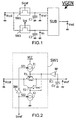
- FIG. 2 is an electrical diagram which represents a storage device (SW1, C1) according to the invention.
- the switch SW1 comprises a first and a second bipolar transistor (T1, T2), whose main current paths, constituted by their collector-emitter junctions, are arranged head to tail between the input and output of the storage device, the switch SW1 being further provided with control means for alternately extracting or injecting current into the bases of the first and second transistors (T1, T2).
- control means include, in this example, a first and a second controllable current source (I1, I2), respectively disposed between the bases of the first and second transistors and a VCC supply terminal and the ground of the device, the bases of the first and second transistors (T1, T2) being short-circuited.
- the conduction of the first and second current sources (I1, I2) is controlled by first and second control signals (SI1, SI2).
- the first control signal SI1 is active, for example at logic level 1
- the second control signal SI2 is inactive, that is to say in this example at logic level 0
- the first current source I1 conducts, and injects a current into the bases of the first and second transistors (T1, T2) which thus become potentially conductive. If the voltage Vccd is greater than the voltage Vref present at the terminals of the capacitive element C1, said element C1 is charged by means of a positive current IC1. It is then the second transistor T2 which is conductive.
- the voltage Vccd is smaller than the voltage Vref present at the terminals of the capacitive element C1, said element C1 discharges by means of a negative current IC1. It is then the first transistor T1 which is conductive. Thus, when the first current source I1 is conductive, the input voltage Vccd is copied across the terminals of the capacitive element C1. When the first current source I1 is conductive, a passing resistance, denoted Ron, appears between the input and output terminals of the storage device.
- Ron is less than ten Ohms, or more than ten times lower than the pass resistance of an NMOS type transistor of similar dimensions.
- the storage device according to the invention therefore generates much less noise than that generated by known devices.
- the second control signal SI2 is active, while the first control signal SI1 is inactive, the second current source I2 conducts, and extracts a current from the bases of the first and second transistors ( T1, T2) whose conduction is thus interrupted almost instantaneously.
- the voltage Vref present at the terminals of the capacitive element C1, representative of the voltage Vccd present at the input terminal during the previous monitoring phase, is thus memorized until the next monitoring phase.
- the first and second control signals SI1 and SI2 can be produced independently of one another outside the storage device (SW1, C1), according to techniques well known to those skilled in the art.
- the storage device includes means for preventing simultaneous conduction of the first and second current sources (I1, I2). These means consist, in this example, of a logic inverter INV, intended to receive as input a single control signal Svref, which here corresponds to the second control signal SI2, and the output of which is intended to deliver the first control signal SI1 .
- the first and second control signals (SI1, SI2) are then permanently in phase opposition, and cannot therefore be active at the same time, which makes it possible to immunize the switch SW1 against any short circuit between the two sources.
- current I1, I2
- the inverter INV may be replaced by delay cells introducing a phase shift of 180 ° between the first and second control signals (SI1, SI2).
- the storage device comprises a voltage regulating element LF disposed between the output terminal and the bases of the first and second transistors (T1, T2), making it possible to limit the amplitude of the base-emitter voltages (Vbe1, Vbe2) first and second transistors (T1, T2).
- the voltage regulating element BF which could for example be of the follower type, ensures that the value of the potential of the bases of the first and second transistors (T1, T2) is of the same order as that of the continuous components of the input signals and output (Vccd, Vref).
- the amplitude of the base-emitter voltages (Vbe1, Vbe2) of the first and second transistors (T1, T2) will therefore remain low, which limits the wear of said transistors and contributes to increasing the life of the storage device.
- this LF regulating element makes it possible to prevent excessively high base-emitter voltages (Vbe1, Vbe2) from inadvertently triggering the conduction of the first and second transistors (T1, T2) when the first current source I1 is not conductive.
- Vbe1, Vbe2 base-emitter voltages
- T1, T2 the first and second transistors
- Such a structure makes it possible to prevent large quantities of charges from propagating in the substrate of the integrated circuit on which the storage device is installed, when the switching operations of the transistors are controlled by strong current pulses. Such propagation phenomena would cause conduction of parasitic junctions existing within the integrated circuit, conduction which would risk destroying said circuit.
- FIG. 4 represents the evolution of signals present in such a camera, in order to facilitate understanding of the invention.
- the input signal Vccd of the generation device VGEN is pseudo-periodic of period T.
- This signal Vccd successively presents, during each pseudo period, a level known as reset RZ, a level called reference REF and a level said VID video.
- reset RZ a level known as reset RZ
- REF a level called reference REF
- the signal Vccd remains at reset level RZ for a predetermined interval [0; t1], and the control signals Svref and Svs are active, which means that the first and second storage devices contained in the generation device VGEN are in the maintenance phase.
- the Vvid video signal delivered by the VGEN generation device is therefore that of the previous pseudo period.
- the signal Vccd takes the reference level REF.
- a time t'1. predetermined, shortly following time t1, a first timeout comes to an end and the control signal Svref becomes inactive. The first storage device then enters the monitoring phase, the second storage device then still being in the maintenance phase.
- a second timeout comes to an end and the control signal Svref becomes inactive again, and the first storage device again enters holding phase, its output signal then representing the new reference level REF.
- a third time delay comes to an end and the control signal Svs becomes inactive. The second storage device then enters the monitoring phase, the second storage device remaining in the maintenance phase.
- a fourth time delay comes to an end and the control signal Svs becomes inactive again, and the second storage device again enters the maintenance phase, its output signal then representing the new video level VID.
- the SUB subtractor the inhibition of which will advantageously have been provided during the interval [t'1;t''2] then delivers a new video signal Vvid representative of the difference between the reference and video levels REF and VID during the period [0; T].
Landscapes
- Picture Signal Circuits (AREA)
- Electronic Switches (AREA)
- Dram (AREA)
- Transforming Light Signals Into Electric Signals (AREA)
Applications Claiming Priority (2)
| Application Number | Priority Date | Filing Date | Title |
|---|---|---|---|
| FR9906299 | 1999-05-18 | ||
| FR9906299A FR2793940A1 (fr) | 1999-05-18 | 1999-05-18 | Dispositif de memorisation a faible bruit et a frequence d'echantillonnage elevee |
Publications (1)
| Publication Number | Publication Date |
|---|---|
| EP1054409A1 true EP1054409A1 (de) | 2000-11-22 |
Family
ID=9545719
Family Applications (1)
| Application Number | Title | Priority Date | Filing Date |
|---|---|---|---|
| EP00201676A Withdrawn EP1054409A1 (de) | 1999-05-18 | 2000-05-10 | Rauscharme Hochabtastfrequenzabtastvorrichtung |
Country Status (5)
| Country | Link |
|---|---|
| US (1) | US6741281B1 (de) |
| EP (1) | EP1054409A1 (de) |
| JP (1) | JP2001014882A (de) |
| FR (1) | FR2793940A1 (de) |
| TW (1) | TW508580B (de) |
Cited By (1)
| Publication number | Priority date | Publication date | Assignee | Title |
|---|---|---|---|---|
| CN114625078A (zh) * | 2016-05-09 | 2022-06-14 | 强力物联网投资组合2016有限公司 | 用于工业物联网的方法和系统 |
Families Citing this family (2)
| Publication number | Priority date | Publication date | Assignee | Title |
|---|---|---|---|---|
| US7245174B2 (en) * | 2004-09-23 | 2007-07-17 | Zetex Plc | Analogue switch |
| GB2418548B (en) * | 2004-09-23 | 2008-08-20 | Zetex Plc | Analogue switch |
Citations (4)
| Publication number | Priority date | Publication date | Assignee | Title |
|---|---|---|---|---|
| FR2078415A5 (de) * | 1970-02-11 | 1971-11-05 | Siemens Ag | |
| US4987321A (en) | 1989-09-25 | 1991-01-22 | Eastman Kodak Company | Processing circuit for image sensor |
| US5027003A (en) | 1989-12-29 | 1991-06-25 | Texas Instruments Incorporated | Read/write switching circuit |
| US5832305A (en) * | 1996-12-02 | 1998-11-03 | Ncr Corporation | Multiple stage analog bi-directional selector utilizing coupled pairs of bi-polar junction transistors connected to pull-up resistors |
Family Cites Families (1)
| Publication number | Priority date | Publication date | Assignee | Title |
|---|---|---|---|---|
| US6018364A (en) * | 1996-02-06 | 2000-01-25 | Analog Devices Inc | Correlated double sampling method and apparatus |
-
1999
- 1999-05-18 FR FR9906299A patent/FR2793940A1/fr active Pending
-
2000
- 2000-05-10 EP EP00201676A patent/EP1054409A1/de not_active Withdrawn
- 2000-05-16 US US09/571,454 patent/US6741281B1/en not_active Expired - Lifetime
- 2000-05-18 JP JP2000146383A patent/JP2001014882A/ja not_active Withdrawn
- 2000-06-22 TW TW089112266A patent/TW508580B/zh not_active IP Right Cessation
Patent Citations (4)
| Publication number | Priority date | Publication date | Assignee | Title |
|---|---|---|---|---|
| FR2078415A5 (de) * | 1970-02-11 | 1971-11-05 | Siemens Ag | |
| US4987321A (en) | 1989-09-25 | 1991-01-22 | Eastman Kodak Company | Processing circuit for image sensor |
| US5027003A (en) | 1989-12-29 | 1991-06-25 | Texas Instruments Incorporated | Read/write switching circuit |
| US5832305A (en) * | 1996-12-02 | 1998-11-03 | Ncr Corporation | Multiple stage analog bi-directional selector utilizing coupled pairs of bi-polar junction transistors connected to pull-up resistors |
Cited By (1)
| Publication number | Priority date | Publication date | Assignee | Title |
|---|---|---|---|---|
| CN114625078A (zh) * | 2016-05-09 | 2022-06-14 | 强力物联网投资组合2016有限公司 | 用于工业物联网的方法和系统 |
Also Published As
| Publication number | Publication date |
|---|---|
| US6741281B1 (en) | 2004-05-25 |
| FR2793940A1 (fr) | 2000-11-24 |
| TW508580B (en) | 2002-11-01 |
| JP2001014882A (ja) | 2001-01-19 |
Similar Documents
| Publication | Publication Date | Title |
|---|---|---|
| EP3140906B1 (de) | Vorrichtung mit hohem dynamikumfang zur integration eines elektrischen stroms | |
| FR2535870A1 (fr) | Circuit d'alimentation en courant electrique d'un micro-ordinateur | |
| EP1263210A1 (de) | Aktiver CMOS-Pixel mit verringertem Geräusch | |
| EP0649079B1 (de) | Geregelter Spannungsquellengenerator der Bandgapbauart | |
| FR2462818A1 (fr) | Circuit pour eviter le declic se produisant lors de l'enclenchement et du declenchement de la tension d'alimentation d'un amplificateur | |
| FR2793940A1 (fr) | Dispositif de memorisation a faible bruit et a frequence d'echantillonnage elevee | |
| EP0230809B1 (de) | Wärmebildkamera mit Parallelabtastung | |
| FR2538193A1 (fr) | Interface de sortie pour circuit logique a trois etats dans un circuit integre a transistors mos | |
| FR3072481B1 (fr) | Dispositif de generation d'un signal aleatoire | |
| EP0156675B1 (de) | Vorladungsschaltung für Digitaldaten-Übertragungsbus | |
| CH635688A5 (fr) | Detecteur photo-electrique de la presence d'un objet. | |
| EP0281465B1 (de) | Speicherleseverstärker | |
| FR2494040A1 (fr) | Dispositif a circuits integres a semiconducteurs proteges contre les surtensions accidentelles | |
| FR2490895A1 (fr) | Circuit d'entretien pour oscillateur a faible consommation de courant | |
| EP1074996B1 (de) | Abtasthalteschaltung | |
| FR3010229A1 (fr) | Capteur d'image avec bruit ktc reduit | |
| FR2518850A1 (fr) | Systeme de reglage d'amplitude | |
| EP0076195B1 (de) | Anordnung zur Stromauslesung einer Ladungsquantität und Ladungsübertragungsfilter mit solch einer Anordnung | |
| EP1330918B1 (de) | Lesevorrichtung für elektromagnetische strahlungen, sensor, und entsprechendes leseverfahren | |
| FR2937150A1 (fr) | Dispositif et procede pour realiser la lecture de courants electriques resultant d'un detecteur de signaux electromagnetiques | |
| FR2802698A1 (fr) | Circuit de lecture de charges protege contre des surcharges provenant de charges de polarite non desiree | |
| FR2767933A1 (fr) | Circuit adaptateur de tension d'alimentation | |
| FR2677771A1 (fr) | Circuit de detection de niveau de polarisation inverse dans un dispositif de memoire a semiconducteurs. | |
| EP0849659B1 (de) | Digitale Rücksetzvorrichtung eines integrierten Schaltkreises | |
| FR2595528A1 (fr) | Dispositif de separation des impulsions de synchronisation d'un signal de television |
Legal Events
| Date | Code | Title | Description |
|---|---|---|---|
| PUAI | Public reference made under article 153(3) epc to a published international application that has entered the european phase |
Free format text: ORIGINAL CODE: 0009012 |
|
| AK | Designated contracting states |
Kind code of ref document: A1 Designated state(s): DE FR GB |
|
| AX | Request for extension of the european patent |
Free format text: AL;LT;LV;MK;RO;SI |
|
| 17P | Request for examination filed |
Effective date: 20010522 |
|
| AKX | Designation fees paid |
Free format text: DE FR GB |
|
| 17Q | First examination report despatched |
Effective date: 20041119 |
|
| RAP1 | Party data changed (applicant data changed or rights of an application transferred) |
Owner name: NXP B.V. |
|
| STAA | Information on the status of an ep patent application or granted ep patent |
Free format text: STATUS: THE APPLICATION IS DEEMED TO BE WITHDRAWN |
|
| 18D | Application deemed to be withdrawn |
Effective date: 20101201 |