EP1056070A2 - Treiberschaltung und Treiberschaltungssystem für kapazitive Last - Google Patents
Treiberschaltung und Treiberschaltungssystem für kapazitive Last Download PDFInfo
- Publication number
- EP1056070A2 EP1056070A2 EP00111318A EP00111318A EP1056070A2 EP 1056070 A2 EP1056070 A2 EP 1056070A2 EP 00111318 A EP00111318 A EP 00111318A EP 00111318 A EP00111318 A EP 00111318A EP 1056070 A2 EP1056070 A2 EP 1056070A2
- Authority
- EP
- European Patent Office
- Prior art keywords
- transistor
- power supply
- voltage
- current
- drive circuit
- Prior art date
- Legal status (The legal status is an assumption and is not a legal conclusion. Google has not performed a legal analysis and makes no representation as to the accuracy of the status listed.)
- Withdrawn
Links
Images












Classifications
-
- G—PHYSICS
- G09—EDUCATION; CRYPTOGRAPHY; DISPLAY; ADVERTISING; SEALS
- G09G—ARRANGEMENTS OR CIRCUITS FOR CONTROL OF INDICATING DEVICES USING STATIC MEANS TO PRESENT VARIABLE INFORMATION
- G09G3/00—Control arrangements or circuits, of interest only in connection with visual indicators other than cathode-ray tubes
- G09G3/20—Control arrangements or circuits, of interest only in connection with visual indicators other than cathode-ray tubes for presentation of an assembly of a number of characters, e.g. a page, by composing the assembly by combination of individual elements arranged in a matrix no fixed position being assigned to or needed to be assigned to the individual characters or partial characters
- G09G3/34—Control arrangements or circuits, of interest only in connection with visual indicators other than cathode-ray tubes for presentation of an assembly of a number of characters, e.g. a page, by composing the assembly by combination of individual elements arranged in a matrix no fixed position being assigned to or needed to be assigned to the individual characters or partial characters by control of light from an independent source
- G09G3/36—Control arrangements or circuits, of interest only in connection with visual indicators other than cathode-ray tubes for presentation of an assembly of a number of characters, e.g. a page, by composing the assembly by combination of individual elements arranged in a matrix no fixed position being assigned to or needed to be assigned to the individual characters or partial characters by control of light from an independent source using liquid crystals
-
- G—PHYSICS
- G09—EDUCATION; CRYPTOGRAPHY; DISPLAY; ADVERTISING; SEALS
- G09G—ARRANGEMENTS OR CIRCUITS FOR CONTROL OF INDICATING DEVICES USING STATIC MEANS TO PRESENT VARIABLE INFORMATION
- G09G3/00—Control arrangements or circuits, of interest only in connection with visual indicators other than cathode-ray tubes
- G09G3/20—Control arrangements or circuits, of interest only in connection with visual indicators other than cathode-ray tubes for presentation of an assembly of a number of characters, e.g. a page, by composing the assembly by combination of individual elements arranged in a matrix no fixed position being assigned to or needed to be assigned to the individual characters or partial characters
- G09G3/34—Control arrangements or circuits, of interest only in connection with visual indicators other than cathode-ray tubes for presentation of an assembly of a number of characters, e.g. a page, by composing the assembly by combination of individual elements arranged in a matrix no fixed position being assigned to or needed to be assigned to the individual characters or partial characters by control of light from an independent source
- G09G3/36—Control arrangements or circuits, of interest only in connection with visual indicators other than cathode-ray tubes for presentation of an assembly of a number of characters, e.g. a page, by composing the assembly by combination of individual elements arranged in a matrix no fixed position being assigned to or needed to be assigned to the individual characters or partial characters by control of light from an independent source using liquid crystals
- G09G3/3611—Control of matrices with row and column drivers
- G09G3/3685—Details of drivers for data electrodes
- G09G3/3688—Details of drivers for data electrodes suitable for active matrices only
-
- G—PHYSICS
- G09—EDUCATION; CRYPTOGRAPHY; DISPLAY; ADVERTISING; SEALS
- G09G—ARRANGEMENTS OR CIRCUITS FOR CONTROL OF INDICATING DEVICES USING STATIC MEANS TO PRESENT VARIABLE INFORMATION
- G09G2310/00—Command of the display device
- G09G2310/02—Addressing, scanning or driving the display screen or processing steps related thereto
- G09G2310/0264—Details of driving circuits
- G09G2310/0291—Details of output amplifiers or buffers arranged for use in a driving circuit
Definitions
- the present invention relates to a drive circuit and a drive circuit system, and more specifically to a drive circuit and a drive circuit system used in a driver or a buffer which constitutes an output stage of a driving circuit for a capacitive load exemplified by a liquid crystal display (LCD).
- LCD liquid crystal display
- a display section of the liquid crystal display of an active matrix driving type includes a semiconductor substrate having transparent pixel electrodes and thin film transistors (TFT) formed thereon, an opposing substrate having a single transparent common electrode formed to cover the whole of a surface of the substrate, and a liquid crystal encapsulated between the two substrates which are located to oppose each other, separately from each other.
- TFTs thin film transistors
- a predetermined voltage is applied to selected pixel electrodes so that a transmittance of the liquid crystal is changed by a potential difference between each pixel electrode and the opposing common electrode.
- data lines for supplying a plurality of different level voltages (gradation voltages) to be selectively applied to each pixel electrode, and scan lines for supplying a switching control signal for each TFT, are located.
- the data lines become a large capacitive load because of a liquid crystal capacitance between the data lines and the opposing common electrode and a capacitance between the data lines and the scan lines that intersect each other. Since the gradation voltage is applied trough the data line to each pixel electrodes, and since the gradation voltages are written to all the pixels connected to the data lines during each one frame period, a data line drive circuit has to rapidly drive a corresponding data line which is a large capacitive load.
- the data line drive circuit is required to rapidly drive a corresponding data line having a large capacitance with a high voltage precision.
- various data line drive circuits have been developed.
- a circuit that has enabled a high voltage precision output and a rapid driving is a drive circuit including a driver (buffer) section formed of an operational amplifier.
- a driver buffer
- FIG. 16 A typical and simplest example will be shown in Fig. 16.
- the operational amplifier shown in Fig. 16 is in the form of a voltage follower, capable of outputting, as an output voltage Vout, a voltage equal to an input voltage Vin.
- the shown operational amplifier is constituted of a differential amplifier stage 610 and an output amplifier stage 620.
- the differential amplifier stage 610 includes a current control circuit 601, PMOS transistors 603 and 604 having the same characteristics, and NMOS transistors 605 and 606 having the same characteristics, which are connected as shown.
- the NMOS transistors 605 and 606 have respective gates connected in common, and respective sources connected in common to a power supply terminal T 14 .
- a drain of the NMOS transistor 606 is connected to the gate of the NMOS transistor 606.
- the PMOS transistors 603 and 604 have respective sources connected in common.
- a gate of the PMOS transistor 603 is connected to an input terminal T 1 to receive the input voltage Vin.
- a drain of the PMOS transistor 603 is connected to a drain of the NMOS transistor 605.
- a gate of the PMOS transistor 604 is connected to an output terminal T 2 for outputting the output voltage Vout.
- a drain of the PMOS transistor 604 is connected to the drain of the NMOS transistor 606.
- the current control circuit 601 is connected between a power supply terminal T 13 and the common-connected sources of the PMOS transistors 603 and 604.
- the output amplifier stage 620 includes a current control circuit 602, an NMOS transistor 607 and a capacitor 608, connected as shown.
- the current control circuit 602 is connected between a power supply terminal T 11 and the output terminal T 2 .
- the NMOS transistor 607 has a drain connected to the output terminal T 2 , a source connected to a power supply terminal T 12 , and a gate connected to the common-connected drains of the PMOS transistor 603 and the NMOS transistor 605.
- the capacitor 608 is connected between the gate of the NMOS transistor 607 and the output terminal T 2 .
- currents controlled by the current control circuits 601 and 602 are called I61 and I62, respectively.
- a voltage V DD is supplied to the power supply terminals T 11 and T 13
- a voltage V SS is supplied to the power supply terminals T 12 and T 14 .
- the output terminal T 2 is connected to the data line, which is a capacitive load.
- the operational amplifier shown in Fig. 16 has a construction having a voltage amplification factor of "1" (one) and a high current supplying capacity (voltage follower).
- a designated or selected gradation voltage is applied as the input voltage Vin during each outputting period, and the operational amplifier can drive the data line connected to the output terminal T 2 and having a large capacitance, by the gradation voltage with a high current supplying capacity.
- the operational amplifier can drive the data line, by action of an impedance conversion, independently of a current supplying capacity of an external circuit supplying the input voltage Vin.
- the operational amplifier shown in Fig. 16 (voltage follower circuit) has a feed-back structure, oscillation often occurs, and therefore, it is necessary to provide the means such as a phase compensation capacitor for preventing the oscillation.
- the phase compensation capacitor often requires a large occupying chip. Therefore, when a number of operational amplifiers are built in a single integrated circuit, a required area of the integrated circuit becomes large, with the result that a production cost adversely increases.
- Another object of the present invention is to provide a drive circuit having a simple circuit construction which can be constituted of only transistors, and capable of stably operating with no oscillation, for rapidly driving a load with a high precision voltage output.
- Still another object of the present invention is to provide a drive circuit and a drive circuit system, which can reduce the production cost when a number of drive circuits are integrated as an integrated circuit.
- a drive circuit comprising a level converting means for level-converting an input voltage into a first voltage, a first transistor having a gate connected to receive the first voltage and a source for outputting an output voltage pursuant to the input voltage, a first current control means for controlling a current flowing through a drain-source path of the first transistor so that the first transistor operates in a source follower fashion, the level converting means including a second transistor of the same conductivity type as that of the first transistor.
- the second transistor has a source connected to receive the input voltage, and a drain and a gate connected in common for outputting the first voltage, and the level converting means also includes a second current control means for controlling a current flowing through a drain-source path of the second transistor.
- a drive circuit comprising a first power supply terminal, an input terminal for receiving an input voltage, an output terminal for outputting an output voltage, a first transistor having a source connected to the input terminal and a drain and a gate connected in common, a second transistor of the same conductivity type as that of the first transistor, the second transistor having a drain connected to the first power supply terminal, a source connected to the output terminal, and a gate connected to receive a voltage equal to a gate voltage of the first transistor, a first current control means for controlling a current flowing through a drain-source path of the first transistor, and a second current control means for controlling a current flowing through a drain-source path of the second transistor.
- the first current control means can include a first current control circuit connected between a second power supply terminal and the drain of the first transistor, and the second current control means can include a second current control circuit connected between the output terminal and a third power supply terminal. Furthermore, a third current control circuit can be connected between the input terminal and a fourth power supply terminal.
- the drive circuit can further include at least a first switch connected in series with the first transistor between the input terminal and the second power supply terminal and on-off controlled for cutting off a current flowing between the input terminal and the second power supply terminal, a second switch connected in series with second current control circuit between the output terminal and the third power supply terminal and on-off controlled for cutting off a current flowing between the output terminal and the third power supply terminal, a third switch connected in series with the third current control circuit between the input terminal and the fourth power supply terminal and on-off controlled for cutting off a current flowing between the input terminal and the fourth power supply terminal, and a fourth switch connected in series with the second transistor between the output terminal and the first power supply terminal and on-off controlled for cutting off a current flowing between the output terminal and the first power supply terminal.
- the drive circuit can further include a first precharging means for precharging the output terminal to at least one predetermined voltage.
- the drive circuit can further include a second precharging means for precharging the gate of the first transistor to a first predetermined voltage.
- the first current control circuit includes a first current controlling transistor having a drain-source path connected between a second power supply terminal and the drain of the first transistor
- the second current control circuit includes a second current controlling transistor having a drain-source path connected between the output terminal and a third power supply terminal.
- the second current controlling transistor is of the conductivity type different from that of the first current controlling transistor.
- the third current control circuit includes a third current controlling transistor having a drain-source path connected between the input terminal and a fourth power supply terminal.
- the third current controlling transistor is of the same conductivity type as that of the second current controlling transistor.
- the drive circuit further includes a bias circuit having a first bias transistor and a second bias transistor connected in series.
- the first bias transistor is of the conductivity type different from that of the second bias transistor.
- the first bias transistor and the second bias transistor have a drain-source path current equal in magnitude to each other.
- the first bias transistor is of the same conductivity type as that of the first current controlling transistor, and has the same gate-source voltage as that of the first current controlling transistor.
- the second bias transistor is of the same conductivity type as that of the second and third current controlling transistors, and has the same gate-source voltage as that of the second and third current controlling transistors.
- a drive circuit system comprising an input terminal for receiving an input voltage, an output terminal for outputting an output voltage, first and second drive circuits each connected to the input terminal and the output terminal,
- the first current control means can include a first current control circuit connected between a third power supply terminal and the drain of the first n-channel transistor
- the second current control means can include a second current control circuit connected between the output terminal and a fourth power supply terminal
- the third current control means can include a third current control circuit connected between a fifth power supply terminal and the drain of the first p-channel transistor
- the fourth current control means includes a fourth current control circuit connected between the output terminal and a sixth power supply terminal.
- the first drive circuit can further include a fifth current control circuit connected between the input terminal and a seventh power supply terminal, and the second drive circuit can include a sixth current control circuit connected between the input terminal and an eight power supply terminal.
- the first drive circuit can further include at least a first switch connected in series with the first n-channel transistor between the input terminal and the third power supply terminal and on-off controlled for cutting off a current flowing between the input terminal and the third power supply terminal, a second switch connected in series with the second current control circuit between the output terminal and the fourth power supply terminal and on-off controlled for cuffing off a current flowing between the output terminal and the fourth power supply terminal, a third switch connected in series with the fifth current control circuit between the input terminal and the seventh power supply terminal and on-off controlled for cutting off a current flowing between the input terminal and the seventh power supply terminal, and a fourth switch connected in series with the second n-channel transistor between the output terminal and the first power supply terminal and on-off controlled for cutting off a current flowing between the output terminal and the first power supply terminal.
- the second drive circuit can further include at least a fifth switch connected in series with the first p-channel transistor between the input terminal and the fifth power supply terminal and on-off controlled for cutting off a current flowing between the input terminal and the fifth power supply terminal, a sixth switch connected in series with the fourth current control circuit between the output terminal and the sixth power supply terminal and on-off controlled for cutting off a current flowing between the output terminal and the sixth power supply terminal, a seventh switch connected in series with the sixth current control circuit between the input terminal and the eighth power supply terminal and on-off controlled for cutting off a current flowing between the input terminal and the eighth power supply terminal, and an eighth switch connected in series with the second p-channel transistor between the output terminal and the second power supply terminal and on-off controlled for cutting off a current flowing between the output terminal and the second power supply terminal.
- the drive circuit system can further include a first precharging means for precharging the output terminal to at least one predetermined voltage.
- the drive circuit system can further include a second precharging means for precharging the gate of the first n-channel transistor to a first predetermined voltage, and a third precharging means for precharging the gate of the first p-channel transistor to a second predetermined voltage.
- a drive circuit apparatus comprising:
- a gate-source voltage of the first transistor is unambiguously determined by a drain-source current of the first transistor. Therefore, if an input voltage Vin is applied to the source of the first transistor, the gate voltage of the first transistor becomes a voltage that is deviated from the input voltage Vin by the gate-source voltage of the first transistor. On the other hand, since the drain of the second transistor receives the power supply voltage and the gate of the second transistor receives the voltage equal to the gate voltage of the first transistor, the second transistor operates in a source follower fashion.
- the gate-source voltage of the second transistor is unambiguously determined, so that an output voltage Vout obtained from the source of the second transistor becomes stable at a voltage which is deviated from the gate voltage of the second transistor by the gate-source voltage of the second transistor.
- the output voltage Vout pursuant to the input voltage Vin.
- the output voltage Vout rapidly changes to a voltage pursuant to the input voltage Vin, by action of the source-follower operation of the second transistor.
- FIG. 1 there is shown a conceptual circuit diagram of the drive circuit in accordance with a first concept of the present invention.
- the shown circuit includes two field effect transistors 1 and 2 which are of the same conductivity type and which have respective gates connected in common.
- the transistor 1 has a drain and the gate connected to each other, and a source connected to an input terminal T 1 .
- the transistor 2 has a drain connected to a power supply terminal T 3 and a source connected to an output terminal T 2 .
- a current control circuit 3 is connected between the power supply terminal T 3 and the drain of the transistor 1, for controlling a current I 1 which flows from the power supply terminal T 3 into the input terminal T 1 .
- a current control circuit 4 is connected between the input terminal T 1 and a power supply terminal T 4 , for controlling a current I 2 which flows from the input terminal T 1 into the power supply terminal T 4 .
- a current control circuit 5 is connected between the output terminal T 2 and the power supply terminal T 4 , for controlling a current I 3 which flows from the output terminal T 2 into the power supply terminal T 4 .
- Voltages E 1 and E 2 are supplied to the power supply terminals T 3 and T 4 , respectively.
- the output terminal T 2 is connected to a capacitive load (not shown) such as the data line.
- the reference sign "s" in Fig. 1 indicates a source terminal of the transistors. This is applied to the other drawings.
- a gate voltage V 1 of the transistor 1 becomes a voltage which is deviated from the input voltage Vin by a gate-source voltage Vgs 1 of the transistor 1.
- V 1 Vin + Vgs 1
- the transistor has an inherent characteristics in a relation between a drain-source current Ids and a gate-source voltage Vgs (called a "Ids-Vgs characteristics" in this specification), so that the gate-source voltage Vgs 1 of the transistor 1 is unambiguously determined by the Ids-Vgs characteristics of the transistor 1 and the current I 1 .
- Vout V 1 - Vgs 2
- This output voltage Vout is stabilized when a drain-source current of the transistor 2 becomes equal to the current I 3 .
- the gate-source voltage Vgs 2 of the transistor 2 in this condition becomes Vgs 2 (I 3 ) that is unambiguously determined by the Ids-Vgs characteristics of the transistor 2 and the current I 3 .
- Vout Vin + Vgs 1 (I 1 ) - Vgs 2 (I 3 )
- an output voltage range becomes a voltage difference between the power supply voltage E 1 and the power supply voltage E 2 , subtracted by at least the gate-source voltage Vgs 2 (I 3 ) of the transistor 2.
- the output voltage Vout becomes equal with the input voltage Vin, as seen from the equation (5). Furthermore, if the device size of the transistors 1 and 2 and the currents I 1 and I 3 are set to maintain the relation of "Vgs 1 (I 1 ) - Vgs 2 (I 3 )" at a constant value even if the characteristics of transistors on the same chip varies, it is possible to supply a highly precise voltage independently of variation in the characteristics of transistors.
- the respective device sizes of the transistors 1 and 2 are set to be equal and the currents I 1 and I 3 are set to be equal, or alternatively, if the respective channel lengths of the transistors 1 and 2 are set to be equal and the currents I 1 and I 3 are set to correspond to the channel widths of the transistors 1 and 2, respectively, it is possible to supply a highly precise voltage independently of variation in threshold voltage of transistors.
- the drive circuit shown in Fig. I can be easily operated.
- the current control circuit 4 was omitted, the drive circuit shown in Fig. 1 can operate. In this case, the external circuit supplying the input voltage Vin is required to have a sufficient current supply capacity.
- the drive circuit shown in Fig. 1 operates as follows:
- the voltage V 1 relatively rapidly follows the change of the input voltage Vin, and changes to the voltage expressed by the equation (2).
- the output voltage Vout rapidly changes to the voltage expressed by the equation (5), by a source follower operation of the transistor 2.
- the transistor 2 is temporarily turned off, the output voltage Vout rapidly changes to the voltage expressed by the equation (5), by the current supplying capacity of the current I 3 .
- the current supplying capacity in the source follower operation of the transistor 2 lowers as the gate-source voltage of the transistor 2 approaches the threshold voltage. But, the source follower operation of the transistor 2 maintains the current supplying capacity corresponding to the current I 3 at minimum.
- the drive circuit shown in Fig. 1 has a high driving capacity obtained by the source follower operation of the transistor 2, and when the input voltage Vin varies to approach die power supply voltage E 2 , the drive circuit shown in Fig. 1 has the driving capacity which depends upon the current I 3 . Therefore, if the current I 3 is adjusted by the current control circuit 5, it is possible to change the driving capacity of the drive circuit shown in Fig. 1.
- the output terminal T 2 is connected to the capacitive load (not shown) such as the data line, the voltage change of the output terminal T 2 results in a charging or discharging of the capacitive load, but the capacitive load can be rapidly driven to a high precision voltage.
- the drive circuit shown in Fig. 1 can have a high driving capacity with a simple construction.
- the device size of the transistors 1 and 2 and the currents I 1 and I 3 are set by considering the characteristics variation of transistors, it is possible to realize a high precision voltage output independent of the characteristics variation of transistors attributable to a device fabricating process and a temperature variation.
- the transistors 1 and 2 are depicted by a schematic electronic symbol indicating a MOS transistor.
- the transistors 1 and 2 are constituted of the other type of field effect transistor, a similar advantage can be obtained in a similar operation.
- a similar advantage can be obtained even if each of the MOS transistors 1 and 2 is replaced with a bipolar transistor by considering that the drain, the gate and the source of the MOS transistors correspond to a collector, a base and an emitter of the bipolar transistor, respectively.
- This can be applied to the following embodiments. Therefore, in the following embodiments, a similar note will be omitted, and only the drive circuits constituted of MOS transistors will be described,
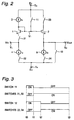
- FIG. 2 there is shown a conceptual circuit diagram of the drive circuit in accordance with a second concept of the present invention.
- the drive circuit shown in Fig. 2 is different in the drive circuit shown in Fig. 1 in the following points:
- a switch 11 is connected between the power supply terminal T 3 and the common-connected gates of the transistors 1 and 2.
- a switch 12 is connected between the power supply terminal T 4 and the output terminal T 2 .
- a switch 21 is connected between the input terminal T 1 and the source of the transistor 1.
- a switch 22 is connected in series with the current control circuit 4 between the input terminal T 1 and the power supply terminal T 4 .
- a switch 23 is connected in series with the transistor 2 between the power supply terminal T 3 and the output terminal T 2 .
- a switch 24 is connected in series with the current control circuit 5 between the output terminal T 2 and the power supply terminal T 4 .
- the output terminal T 2 is connected to a capacitive load (not shown) such as the data line.
- Fig. 3 is a timing chart illustrating an operation of the circuit shown in Fig. 2, during one output period for outputting a selected voltage level.
- the switches 11 and 12 are turned on, and the switches 21, 22, 23 and 24 are turned off.
- the common-connected gates of the transistors 1 and 2 are precharged to the power supply voltage E 1
- the output terminal T 2 is precharged to the power supply voltage E 2 .
- the switch 11 is turned off, and the switches 21 and 22 are turned on.
- the voltage V 1 at the common-connected gates of the transistors 1 and 2 rapidly changes to a voltage which is deviated from the input voltage Vin by the gate-source voltage of the transistor 1, and becomes stable at the voltage expressed by the equation (2).
- the switch 12 is turned off, and the switches 23 and 24 are turned on.
- the output voltage Vout rapidly changes to the voltage expressed by the equation (5), and is maintained at the voltage expressed by the equation (5) until a time t3.
- the drive circuit shown in Fig. 2 has an output voltage range similar to that of the drive circuit shown in Fig. 1.
- the currents I 1 and I 3 are controlled to equalize the gate-source voltages Vgs 1 (I 1 ) and Vgs 2 (I 3 ) of the transistors 1 and 2, the output voltage Vout becomes equal with the input voltage Vin.
- the device size of the transistors 1 and 2 and the currents I 1 and I 3 are set by taking a characteristics variation of transistors into consideration, it is possible to supply a highly precise voltage independently of the characteristics variation of transistors.
- the drive circuit shown in Fig. 2 can be easily operated.
- the drive circuit shown in Fig. 2 can be considered to be improvement to the drive circuit shown in Fig. 1, since the power consumption can be reduced without lowering the driving capacity.
- the drive circuit shown in Fig. 1 when the input voltage Vin varies to approach the power supply voltage E 2 , the drive circuit has the driving capacity depending upon the current I 3 . If the current I 3 is made large, a static power consumption increases.
- the drive circuit when the input voltage Vin varies to approach the power supply voltage E 1 , the drive circuit has a high driving capacity given by the source follower operation of the transistor 2. In the drive circuit shown in Fig.
- the output terminal T 2 is precharged to the power supply voltage E 2 , so that the voltage output of each one output period is obtained by the high driving capacity given by the source follower operation of the transistor 2.
- the precharged voltage of the output terminal T 2 is not limited to only the power supply voltage E 2 , if it is a voltage which enables the transistor 2 to operate in the source follower fashion during a period from the time t2 to the time t3. Therefore, it is possible to provide a plurality of precharging voltage supplies corresponding to a plurality of different input voltages Vin supplied to the input terminal T 1 .
- the precharging of the common-connected gates of the transistors 1 and 2 given by the switch 11 is not necessarily required.
- the current I 1 is limited to an extremely small value, the charging/discharging of the gate capacitance of the transistors 1 and 2 in response to the change of the input voltage Vin needs a substantial time, with the result that the voltage of the common-connected gates of the transistors 1 and 2 cannot be rapidly changed to the voltage V 1 expressed by the equation (2).
- the transistor 1 operates in a source follower fashion, with the result that the voltage of the common-connected gates of the transistors 1 and 2 can be rapidly changed to the voltage V 1 expressed by the equation (2).
- the switches 21, 22, 23 and 24 are controlled to cut off different currents flowing between the input terminal T 1 and the output terminal T 2 and the power supply terminals T 3 and T 4 , during respective precharge times given by the switches 11 and 12. With this arrangement, it is possible to cut off a superfluous current, and therefore to minimize the power consumption caused by the precharging.
- the drive circuit shown in Fig. 2 can operate passably.
- the gate-source voltage of the transistors 1 and 2 becomes almost the threshold voltage so that the drain-source current hardly flows, the voltage V 1 and the output voltage Vout are stabilized.
- another problem would be encountered in that in the neighborhood of the threshold voltage, the change of the drain-source current responding to the change of the gate-source voltage is slow, and therefore, a long time is required until the voltage V 1 and the output voltage Vout are stabilized.
- the drive circuit shown in Fig. 2 can ceaselessly have a high driving capacity by precharging the output terminal T 2 , and simultaneously can realize a low power consumption by limiting the currents I 1 , I 2 and I 3 .
- Fig. 4 is a circuit diagram of the specific embodiment of the drive circuit shown in Fig. 2.
- the transistors 1 and 2 shown in Fig. 2 are constituted of NMOS (n-channel MOS) transistors 101 and 102, respectively.
- the power supply voltages E 1 and E 2 are V DD and V SS , respectively, where V DD > V SS .
- the current control circuits 3,4 and 5 shown in Fig. 2 are respectively realized by current control circuits 103, 104 and 105, which control the currents to I 11 , I 12 and I 13 , respectively.
- the switches 11, 12, 21, 22, 23 and 24 shown in Fig. 2 are respectively realized by switches 111, 112, 121, 122, 123 and 124, which are controlled similarly to the switches 11, 12, 21, 22, 23 and 24 shown in Fig. 3.
- the output terminal T 2 is connected to a capacitive load (not shown) such as the data line.
- a voltage on common-connected gates of the transistors 101 and 102 is called V 10 .
- Fig. 5A is a timing chart for controlling the switches 111, 112, 121, 122, 123 and 124 shown in Fig. 4, and Fig. 5B is a voltage waveform diagram of the input voltage Vin, the output voltage Vout and the voltage V 10 in the circuit shown in Fig. 4.
- One output period for outputting a selected voltage level is shown in Figs. 5A and 5B, and a process for outputting a voltage equal to the input voltage Vin as the output voltage Vout is illustrated in Fig. 5B.
- Vgs 101 (I 11 ) and Vgs 102 (I 13 ) are positive values. If the currents I 11 and I 13 are controlled to equalize Vgs 101 (I 11 ) and Vgs 102 (I 13 ), the output voltage Vout becomes equal to the input voltage Vin, as seen from the equations (6) and (7). At this time, an output voltage range is expressed as follows: V SS ⁇ Vout ⁇ V DD - Vgs 102 (I 13 )
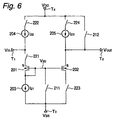
- Fig. 6 is a circuit diagram of another specific embodiment of the drive circuit shown in Fig. 2.
- the transistors 1 and 2 shown in Fig. 2 are constituted of PMOS (p-channel MOS) transistors 201 and 202, respectively.
- the power supply voltages E 1 and E 2 are V SS and V DD , respectively, where V DD > V SS .
- the current control circuits 3, 4 and 5 shown in Fig. 2 are respectively realized by current control circuits 203, 204 and 205, which control the currents to I 21 , I 22 and I 23 , respectively.
- the switches 11, 12, 21, 22, 23 and 24 shown in Fig. 2 are respectively realized by switches 211, 212, 221, 222, 223 and 224, which are controlled similarly to the switches 11, 12, 21, 22, 23 and 24 shown in Fig. 3.
- the output terminal T 2 is connected to a capacitive load (not shown) such as the data line.
- a voltage on common-connected gates of the transistors 201 and 202 is called V 20 .
- Fig. 7A is a timing chart for controlling the switches 211, 212, 221, 222, 223 and 224 shown in Fig. 6, and Fig. 7B is a voltage waveform diagram of the input voltage Vin, the output voltage Vout and the voltage V 20 in the circuit shown in Fig. 6.
- One output period for outputting a selected voltage level is shown in Figs. 7A and 7B, and a process for outputting a voltage equal to the input voltage Vin as the output voltage Vout is illustrated in Fig. 7B.
- Vgs 201 (I 21 ) and Vgs 202 (I 23 ) are negative values. If the currents I 21 and I 23 are controlled to equalize Vgs 201 (I 21 ) and Vgs 202 (I 23 ), the output voltage Vout becomes equal to the input voltage Vin, as seen from the equations (9) and (10). At this time, an output voltage range is expressed as follows: V SS - Vgs 202 (I 23 ) ⁇ Vout ⁇ V DD
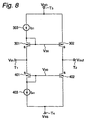
- the shown drive circuit includes two n-channel transistors 301 and 302 having respective gates connected in common, and two p-channel transistors 401 and 402 having respective gates connected in common.
- the transistor 301 has a drain and the gate connected to each other, and a source connected to an input terminal T 1 .
- the transistor 302 has a drain connected to a power supply terminal T 3 and a source connected to an output terminal T 2 .
- the transistor 401 has a drain and the gate connected to each other, and a source connected to the input terminal T 1 .
- the transistor 402 has a drain connected to a power supply terminal T 4 and a source connected to the output terminal T 2 .
- a current control circuit 303 is connected between the power supply terminal T 3 and the drain of the transistor 301, for controlling a current I 31 which flows from the power supply terminal T 3 into the input terminal T 1 .
- a current control circuits 403 is connected between the power supply terminal T 4 and the drain of the transistor 401, for controlling a current I 41 which flows from the input terminal T 1 into the power supply terminal T 4 .
- Voltages V DD and V SS are supplied to the power supply terminals T 3 and T 4 , respectively, where V DD > V SS .
- the output terminal T 2 is connected to a capacitive Load (not shown) such as the data line.
- the output voltage Vout becomes a voltage deviated from the voltages V 30 and V 40 by respective gate-source voltages of the transistors 302 and 402, and is stabilized when respective drain-source currents of the transistors 302 and 402 become equal to each other.
- an output voltage range becomes a voltage difference between the voltage V DD and the voltage V SS , subtracted by the respective gate-source voltages of the transistors 302 and 402.
- the output voltage Vout becomes equal to the input voltage Vin.
- the drive circuit shown in Fig. 8 can be easily operated.
- the drive circuit shown in Fig. 8 can have a high drive capacity.
- the drive circuit shown in Fig. 8 has both a performance obtained in the case that the transistors 1 and 2 in the drive circuit shown in Fig. 1 are constituted of NMOS transistors, and a performance obtained in the case that the transistors 1 and 2 in the drive circuit shown in Fig. 1 are constituted of PMOS transistors,
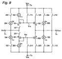
- FIG. 9 there is shown a circuit diagram of an embodiment of the drive circuit in accordance with a fourth concept of the present invention.
- the drive circuit shown in Fig. 9 is one obtained by combining the drive circuit shown in Fig. 4 and the drive circuit shown in Fig. 6 in such a manner that the input terminal T 1 and the output terminal T 2 of the drive circuit shown in Fig. 4 are connected to the input terminal T 1 and the output terminal T 2 of the drive circuit shown in Fig. 6, respectively, and the power supply terminal to be supplied with the voltage V DD and the power supply terminal to be supplied with the voltage V SS in the drive circuit shown in Fig.
- the power supply terminal to be supplied with the voltage V DD is given with T 3
- the power supply terminal to be supplied with the voltage V SS is given with T 4 .
- the output terminal T 2 is connected to a capacitive load (not shown) such as the data line.
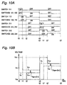
- Fig. 10A is a timing chart illustrating an operation of the circuit shown in Fig. 9, during one output period (time t0 to t3) for outputting a selected voltage level of not greater than Vm, and during another output period (time t0' to t3') for outputting a selected voltage level of not less than Vm.
- Vm is a voltage between V DD and V SS .
- Fig. 10B is a voltage waveform diagram illustrating an operation of the circuit shown in Fig.
- the switches 111, 112, 121, 122, 123 and 124 are on-off controlled, similarly to Fig. 5A, and on the other hand, the switches 211, 212, 221, 222, 223 and 224 are maintained in an off condition. Therefore, the input voltage Vin, the voltage V 10 and the output voltage Vout shown in Fig. 10B become similar to the waveform shown in Fig. 5B. Prom a time t0' to a time t3', the switches 211, 212, 221, 222, 223 and 224 are on-off controlled, similarly to Fig.
- the drive circuit shown in Fig. 9 is constructed to operate the drive circuit shown in Fig. 4 when a selected voltage level of not greater than Vm is to be outputted, and to operate the drive circuit shown in Fig. 6 when a selected voltage level of not less than Vm is to be outputted. Therefore, the drive circuit shown in Fig. 9 has the same driving capacity as those of the drive circuit shown in Fig. 4 and the drive circuit shown in Fig. 6. In addition, in the case of outputting the output voltage Vout equal to the input voltage Vin, the drive circuit shown in Fig. 9 has an output voltage range, expressed by the equation (8) when the drive circuit shown in Fig. 4 operates and expressed by the equation (11) when the drive circuit shown in Fig. 6 operates.
- V SS - Vgs 202 (I 23 ) Vm ⁇ V DD - Vgs 102 (I 13 )
- Vout V SS ⁇ Vout ⁇ V DD
- the output voltage range of the drive circuit shown in Fig. 9 becomes equal to a voltage range of a power supply.
- the drive circuit shown in Fig. 9 when the drive circuit shown in Fig. 9 outputs a selected voltage level of not greater than Vm, the output terminal T 2 is precharged to the voltage V SS , and when the drive circuit shown in Fig. 9 outputs a selected voltage level of not less than Vm, the output terminal T 2 is precharged to the voltage V DD . Therefore, in comparison with the drive circuits shown in Fig. 4 and 6 in which the output terminal T 2 is precharged to only one of the power supply voltage V SS and the power supply voltage V DD , the drive circuit shown in Fig. 9 has a small charging/discharging power for the precharging, and accordingly, can quicken the precharging.
- the drive circuit shown in Fig. 9 has the same driving capacity as those of the drive circuits shown in Fig. 4 and 6, and the output voltage range equal to the voltage range of the power supply, and also can further reduce the power consumption in comparison with the drive circuits shown in Fig. 4 and 6.
- each of the current control circuits 104, 105 and 203 in the drive circuit shown in Fig. 9 is formed of an NMOS transistor, and each of the current control circuits 103, 204 and 205 in the drive circuit shown in Fig. 9 is formed of a PMOS transistor.
- the respective currents I 11 , I 12 , I 13 , I 21 , I 22 and I 23 can be controlled to desired values.
- the output terminal T 2 is connected to a capacitive load (not shown) such as the data line.
- the gates of those current control transistors 104, 105 and 203 are connected to a terminal T 6 supplied with a bias voltage BIASN, and the gates of those current control transistors 103 and 204 and 205 are connected to a terminal T 5 supplied with a bias voltage BIASP.
- the gate bias voltages of a plurality of current control transistors are the same, if the size of each of the current control transistors is adjusted, each of the current control transistors can flow the current of an arbitrary value independent of that of the other current control transistors. It would be a matter of course to persons skilled in the art that it is possible to supply a different bias voltage to each of the current control transistors.
- Fig. 12 is a circuit diagram of a modification of the embodiment of the drive circuit shown in Fig. 11.
- the drive circuit shown in Fig. 12 is improved to be constituted of circuit elements of the number smaller than that of the circuit elements included in the drive circuit shown in Fig. 11 so that the number of the kinds of switch control signals is reduced in comparison with the drive circuit shown in Fig. 11.
- the drive circuit shown in Fig. 12 is different from the drive circuit shown in Fig. 11 in that the current control circuits 104 and 204 and the switches 122 and 222 included in the drive circuit shown in Fig. 11 are omitted, and a PMOS transistor 131 and an NMOS transistor 231 are newly added.
- the PMOS transistor 131 includes a source and a drain connected to the drain (gate) and the source of the NMOS transistor 101, respectively, and a gate connected to the terminal T 5 supplied with the voltage BIASP.
- the NMOS transistor 231 includes a source and a drain connected to the drain (gate) and the source of the PMOS transistor 201, respectively, and a gate connected to the terminal T 6 supplied with the voltage BIASN.
- the PMOS transistor 131 has a threshold voltage smaller than that of the PMOS transistor 103, so that the same gate voltage is applied to the PMOS transistors 103 and 131, the PMOS transistor 131 has a current supplying capacity sufficiently larger than that of the PMOS transistor 103.
- the NMOS transistor 231 has a threshold voltage smaller than that of the NMOS transistor 203, so that the same gate voltage is applied to the NMOS transistors 203 and 231, the NMOS transistor 231 has a current supplying capacity sufficiently larger than that of the NMOS transistor 203.
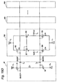
- a circuit constituted of the NMOS transistor 101 and the PMOS transistors 103 and 131 is called a circuit block 130
- a circuit constituted of the PMOS transistor 201 and the NMOS transistors 203 and 231 is called a circuit block 230.
- the output terminal T 2 is connected to a capacitive load (not shown) such as the data line.
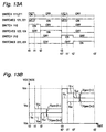
- Fig. 13A is a timing chart illustrating an operation of the circuit shown in Fig. 12, during one output period (time t0 to t3) for outputting a selected voltage level of not greater than Vm, and during another output period (time t0' to t3') for outputting a selected voltage level of not less than Vm.
- Fig. 13B is a voltage waveform diagram illustrating an operation of the circuit shown in Fig. 12, in the case of outputting the output voltage Vout equal to the input voltage Vin.
- on-off timings of the switches 112, 123, 124, 212, 223 and 224 are the same as those shown in Fig. 10A.
- the drive circuit shown in Fig. 12 is featured in that, from a time t0 to a time t3, the circuit block 230 and the switch 221 exercise the same function as that realized in the current control circuit 104 and the switch 122 of the drive circuit shown in Fig. 11, and from a time t0' to a time t3', the circuit block 130 and the switch 121 exercise the same function as that realized in the current control circuit 204 and the switch 222 of the drive circuit shown in Fig. 11. In the following, the operation of the drive circuit shown in Fig. 12 will be described.
- the switches 111 and 211 are turned on, and the switches 121 and 221 are turned off.
- the common-connected gates of the transistors 101 and 102 are precharged to the voltage V DD
- the common-connected gates of the transistors 201 and 202 are precharged to the voltage V SS .
- the switch 112 is turned on and the switches 123 and 124 are turned off, so that the output terminal T 2 is precharged to the voltage V SS .
- the switches 212, 223 and 224 are maintained in an off condition during the period of the time t0 to the time t3.
- the transistors 131 and 231 are brought into the off condition.
- the current I 11 flows between the power supply terminal T 3 and the input terminal T 1
- the current I 21 flows between the input terminal T 1 and the power supply terminal T 4 .
- the switch 112 is turned off, and the switches 123 and 124 are turned on.
- the output voltage Vout rapidly changes to a voltage which is deviated from the voltage V 10 by the gate-source voltage of the transistor 102, and is stabilized at the voltage expressed by the following equation (18) until a time t3.
- Vout V 10 - Vgs 102 (I 13 )
- the output voltage Vout becomes equal to the input voltage Vin.
- the switches 111 and 211 are turned on, and the switches 121 and 221 are turned off.
- the common-connected gates of the transistors 101 and 102 are precharged to the voltage V DD
- the common-connected gates of the transistors 201 and 202 are precharged to the voltage V SS .
- the switch 212 is turned on and the switches 223 and 224 are turned off, so that the output terminal T 2 is precharged to the voltage V DD .
- the switches 112, 123 and 124 are maintained in the off condition during the period of the time t0' to the time t3'.
- the switches 111 and 211 are turned off, and the switches 121 and 221 are turned on.
- the voltage V 10 at the common-connected gates of the transistors 101 and 102 and the voltage V 20 at the common-connected gates of the transistors 201 and 202 respectively rapidly change to the voltages which are deviated from the input voltage Vin by the gate-source voltage of the respective transistor, and become stable at the voltages expressed by the equations (16) and (17).
- the transistors 131 and 231 are brought into the off condition.
- the current I 11 flows between the power supply terminal T 3 and the input terminal T 1
- the current I 21 flows between the input terminal T 1 and the power supply terminal T 4 .
- the switch 212 is turned off, and the switches 223 and 224 are turned on.
- the output voltage Vout rapidly changes to a voltage which is deviated from the voltage V 20 by the gate-source voltage of the transistor 202, and is stabilized at the voltage expressed by the following equation (19) until a time t3'.
- Vout V 20 - Vgs 202 (I 23 )
- the output voltage Vout becomes equal to the input voltage Vin.
- the drive circuit shown in Fig. 12 can be easily operated.
- the above mentioned operation is in the case that the input voltage Vin is higher than the voltage V SS at some degree and lower than the voltage V DD at some degree so that the both of the transistors 101 and 201 are turned on.
- an operation will be described in the case that the input voltage Vin is near to either the voltage V SS or the voltage V DD so that either the transistor 101 or the transistor 201 remains off.
- the voltage V 20 is at the voltage V SS which was precharged during the period from the time t0 to the time t1, but since the current is supplied from the input terminal T 1 to the drain of the transistor 203 by action of the transistor 231, the voltage V 20 is pulled up to an intermediate voltage between the input voltage Vin and the voltage V SS .
- the current supplying capacity of the transistor 231 is larger than that of the transistor 203, the current flowing from the input terminal T 1 to the power supply terminal T 4 becomes the current I 21 controlled by the current control transistor 203. Accordingly, even if the input voltage Vin is near to the voltage V SS so that the transistor 201 remains off, it is possible to supply the current I 21 between the input terminal T 1 and the power supply terminal T 4 .
- the voltage V 10 is at the voltage V DD which was precharged during the period from the time t0' to the time t1, but since the current is supplied from the drain of the transistor 103 to the input terminal T 1 by action of the transistor 131, the voltage V 10 is pulled down to an intermediate voltage between the input voltage Vin and the voltage V DD .
- the current supplying capacity of the transistor 131 is larger than that of the transistor 103, the current flowing from the power supply terminal T 3 to the input terminal T 1 becomes the current I 11 controlled by the current control transistor 103. Accordingly, even if the input voltage Vin is near to the voltage V DD so that the transistor 101 remains off, it is possible to supply the current I 11 between the power supply terminal T 3 and the input terminal T 1 .
- the circuit blocks 130 and 230 can flow the currents I 11 and I 21 , respectively, independently of the voltage level of the input voltage Vin, and also have the function of the current control circuit.
- the switch 221 and the circuit block 230 exercise the same function as that achieved by the switch 122 and the current control circuit 104 of the drive circuit shown in Fig. 11, and during the period from the time t1' to the time t3', the switch 121 and the circuit block 130 exercise the same function as that achieved by the switch 222 and the current control circuit 204 of the drive circuit shown in Fig. 11. Accordingly, the overall basic operation of the drive circuit shown in Fig. 12 is completely the same as that of the drive circuit shown in Fig. 11, and the performance of the drive circuit shown in Fig. 12 is substantially equal to that of the drive circuit shown in Fig. 11.
- a circuit block 500 is the drive circuit in accordance with the present invention in which each current control circuit is constituted of a single current control transistor, and a circuit block 30 is a bias circuit for precisely controlling the current control transistor.
- the circuit block 500 is the drive circuit shown in Fig. 1 in which the transistors 1 and 2 are formed of NMOS transistors 501 and 502, respectively, and the current control circuits 3, 4 and 5 are formed of a PMOS transistor 503 and NMOS transistors 504 and 505, respectively.
- a gate of the PMOS transistor 503 is connected to a terminal T 5 of the circuit block 30, and respective gates of the NMOS transistors 504 and 505 are connected in common to a terminal T 6 of the circuit block 30.
- the power supply terminals T 3 and T 4 are supplied with the power supply voltages V DD and V SS , respectively.
- the output terminal T 2 is connected to a capacitive load (not shown) such as the data line.
- the circuit block 30 is the bias circuit for supplying bias voltages to the respective gates of the transistors 503, 504 and 505 which functions as the current control circuits.
- This bias circuit 30 includes NMOS transistors 31 and 32 and PMOS transistors 33 and 34, as shown.
- the PMOS transistors 33 and 34 have the same Ids-Vgs characteristics.
- the NMOS transistor 31 has a drain connected to the terminal T 5 , a source connected to a power supply terminal T 8 and a gate connected to receive an external bias voltage BIAS.
- the NMOS transistor 32 has a drain and a gate connected in common to the terminal T 6 , and a source connected to the power supply terminal T 8 .
- the PMOS transistor 33 has a drain and a gate connected in common to the terminal T 5 , and a source connected to a power supply terminal T 7 .
- the PMOS transistor 34 has a drain connected to the terminal T 6 , a source connected to the power supply terminal T 7 and a gate connected to the terminal T 5 . Since the PMOS transistors 33 and 34 have the same Ids-Vgs characteristics and the respective gates connected in common, respective drain-source currents of the PMOS transistors 33 and 34 are equal. Here, the drain-source currents of the PMOS transistors 33 and 34 are called an I 4 .
- This current I 4 is controlled by the external bias voltage BIAS, and respective voltages BIASP and BIASN at the terminals T 5 and T 6 are controlled by the current I 4 .
- the power supply terminals T 7 and T 8 are supplied with the power supply voltages V DD and V SS , respectively.
- the drive circuit can be made independent of a current supplying capacity of an external circuit supplying the input voltage Vin.
- the device sizes of the PMOS transistors 33, 34 and 503 and the NMOS transistors 32 and 505 are designed by considering a characteristics variation of transistors and the currents I 4 , I 51 and I 53 are set to equalize respective gate-source voltages of the transistors 501 and 502, even if the characteristics of the transistors varies, it is possible to supply the output voltage Vout equal to the input voltage Vin.
- the transistors 501 and 502 have the same device size
- the PMOS transistors 33, 34 and 503 have the same device size
- the NMOS transistors 32, 504 and 505 have the same device size.
- the currents I 4 , I 51 , I 52 and I 53 are equal, and even if the characteristics of transistors varies, the relation among the currents I 4 , I 51 , I 52 and I 53 is maintained. Accordingly, the drive circuit can output the output voltage Vout equal to the input voltage Vin, independently of a current supplying capacity of an external circuit supplying the input voltage Vin.
- the drive circuit 500 is made independent of a current supplying capacity of an external circuit supplying the input voltage Vin, and the drive circuit 500 can output a highly precise voltage, independently of characteristics variation of transistors attributable to a device fabricating process and a temperature variation.
- FIG. 15A there is shown a circuit diagram of a modification of the current control circuit shown in Fig. 14A.
- a bias circuit 40 shown in Fig. 15A is different from the bias circuit 30 shown in Fig. 14A in that the transistors 31 and 33 are omitted to reduce the current amount flowing in the bias circuit.
- the external bias voltage BIAS is applied directed to the drive circuit 500 and the gate of the transistor 34 in the bias circuit 40, as the bias voltage BIASP, and the current I 4 is controlled by the external bias voltage BIAS.
- the drive circuit can be made independent of a current supplying capacity of an external circuit supplying the input voltage Vin.
- the device sizes of the PMOS transistors 34 and 503 and the NMOS transistors 32 and 505 are designed by considering a characteristics variation of transistors and the currents I 4 , I 51 and I 53 are set to equalize respective gate-source voltages of the transistors 501 and 502, even if the characteristics of transistors varies, it is possible to supply the output voltage Vout equal to the input voltage Vin.
- an advantageous operation similar to that obtained in the bias circuit 30 can be obtained.
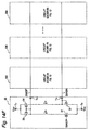
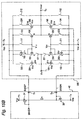
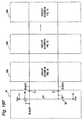
- the drive circuit 500 shown in Figs. 14A and 15A can be replaced with the drive circuit shown in Fig. 11 or 12, as shown in Figs. 14B and 14C and Figs. 15B and 15C, or alternatively, another embodiment of the drive circuit.
- one bias circuit 30 or 40 is provided for only one drive circuit 500.
- one bias circuit 30 or 40 can be provided in common to the plurality of drive circuits 500, as shown in Figs. 14D, 14E and 14F and Figs. 15D, 15E and 15F.
- the drive circuit in accordance with the present invention has a very simple circuit construction including a pair of transistors having respective gates connected in common, the gate of a first transistor being connected to a drain of the first transistor itself, and a second transistor being operated in a source-follower fashion.
- the drive circuit can drive a capacitive load with a high current supplying capacity.
- the drive circuit in accordance with the present invention is in no way limited to the driving of the liquid crystal display (LCD), but can be effectively used for driving other data lines (which constitutes a capactive load) such as data lines for a TFT-OLED (thin film transistor - organic light emitting diode) display in which a plurality of different voltage levels corresponding to a plurality of gradation levels are selectively supplied to each data.
- LCD liquid crystal display
- TFT-OLED thin film transistor - organic light emitting diode
Landscapes
- Engineering & Computer Science (AREA)
- Theoretical Computer Science (AREA)
- Physics & Mathematics (AREA)
- Crystallography & Structural Chemistry (AREA)
- Computer Hardware Design (AREA)
- General Physics & Mathematics (AREA)
- Chemical & Material Sciences (AREA)
- Control Of Indicators Other Than Cathode Ray Tubes (AREA)
- Liquid Crystal (AREA)
- Liquid Crystal Display Device Control (AREA)
- Electronic Switches (AREA)
- Oscillators With Electromechanical Resonators (AREA)
- Amplifiers (AREA)
Applications Claiming Priority (2)
| Application Number | Priority Date | Filing Date | Title |
|---|---|---|---|
| JP14576899A JP3482908B2 (ja) | 1999-05-26 | 1999-05-26 | 駆動回路、駆動回路システム、バイアス回路及び駆動回路装置 |
| JP14576899 | 1999-05-26 |
Publications (2)
| Publication Number | Publication Date |
|---|---|
| EP1056070A2 true EP1056070A2 (de) | 2000-11-29 |
| EP1056070A3 EP1056070A3 (de) | 2002-01-09 |
Family
ID=15392724
Family Applications (1)
| Application Number | Title | Priority Date | Filing Date |
|---|---|---|---|
| EP00111318A Withdrawn EP1056070A3 (de) | 1999-05-26 | 2000-05-25 | Treiberschaltung und Treiberschaltungssystem für kapazitive Last |
Country Status (5)
| Country | Link |
|---|---|
| US (1) | US6624669B1 (de) |
| EP (1) | EP1056070A3 (de) |
| JP (1) | JP3482908B2 (de) |
| KR (1) | KR100385780B1 (de) |
| TW (1) | TW525126B (de) |
Cited By (3)
| Publication number | Priority date | Publication date | Assignee | Title |
|---|---|---|---|---|
| EP1223671A3 (de) * | 2000-12-28 | 2004-08-11 | Nec Corporation | Verstärkerschaltung mit Rückkopplung und Treiberschaltung |
| EP1274067A3 (de) * | 2001-07-06 | 2009-02-25 | Nec Corporation | Treiberschaltung |
| CN111756365A (zh) * | 2019-03-28 | 2020-10-09 | 拉碧斯半导体株式会社 | 半导体装置和数据驱动器 |
Families Citing this family (19)
| Publication number | Priority date | Publication date | Assignee | Title |
|---|---|---|---|---|
| JP4183222B2 (ja) | 2000-06-02 | 2008-11-19 | 日本電気株式会社 | 携帯電話機の省電力駆動方法 |
| JP4929431B2 (ja) * | 2000-11-10 | 2012-05-09 | Nltテクノロジー株式会社 | パネル表示装置のデータ線駆動回路 |
| JP3730886B2 (ja) | 2001-07-06 | 2006-01-05 | 日本電気株式会社 | 駆動回路及び液晶表示装置 |
| US7102608B2 (en) * | 2002-06-21 | 2006-09-05 | Himax Technologies, Inc. | Method and related apparatus for driving pixels located in a row of an LCD panel toward the same average voltage value |
| US6977549B2 (en) * | 2002-02-25 | 2005-12-20 | Nec Corporation | Differential circuit, amplifier circuit, driver circuit and display device using those circuits |
| JP4252855B2 (ja) * | 2002-11-06 | 2009-04-08 | アルプス電気株式会社 | ソースフォロア回路および液晶表示装置の駆動装置 |
| JP2006506680A (ja) * | 2002-11-15 | 2006-02-23 | コーニンクレッカ フィリップス エレクトロニクス エヌ ヴィ | 予備充電装置を備える表示装置 |
| JP2004361424A (ja) * | 2003-03-19 | 2004-12-24 | Semiconductor Energy Lab Co Ltd | 素子基板、発光装置及び発光装置の駆動方法 |
| JP4353759B2 (ja) | 2003-09-22 | 2009-10-28 | Necエレクトロニクス株式会社 | 駆動回路 |
| EP1619688A1 (de) * | 2004-07-21 | 2006-01-25 | Dialog Semiconductor GmbH | Speicher mit dynamisch vorgespanntem Abtastverstärker |
| US7208974B1 (en) * | 2004-09-27 | 2007-04-24 | Marvell International Ltd. | Rail-to-rail source followers |
| EP1815304B1 (de) * | 2004-11-16 | 2010-10-27 | Nxp B.V. | Vorrichtung zur filterung einer referenzspannung und mobiltelefone mit dieser vorrichtung |
| TWI296405B (en) * | 2005-08-19 | 2008-05-01 | Toppoly Optoelectronics Corp | Source-follower type analogue buffer, driving method thereof, and display therwith |
| US7423476B2 (en) * | 2006-09-25 | 2008-09-09 | Micron Technology, Inc. | Current mirror circuit having drain-source voltage clamp |
| JP2008139697A (ja) | 2006-12-04 | 2008-06-19 | Nec Electronics Corp | 容量性負荷駆動回路および容量性負荷駆動方法、液晶表示装置駆動方法 |
| WO2014077200A1 (ja) * | 2012-11-13 | 2014-05-22 | ソニー株式会社 | 表示装置及び表示装置の駆動方法、並びに、信号出力回路 |
| US9172363B2 (en) * | 2013-10-25 | 2015-10-27 | Infineon Technologies Austria Ag | Driving an MOS transistor with constant precharging |
| CN103854587B (zh) * | 2014-02-21 | 2017-03-01 | 北京大学深圳研究生院 | 栅极驱动电路及其单元和一种显示器 |
| US10483976B1 (en) * | 2018-05-24 | 2019-11-19 | Texas Instruments Incorporated | Circuits to interpret pin inputs |
Family Cites Families (21)
| Publication number | Priority date | Publication date | Assignee | Title |
|---|---|---|---|---|
| JPS5990412A (ja) * | 1982-11-15 | 1984-05-24 | Nec Corp | 双方向性定電流駆動回路 |
| JPS61212907A (ja) | 1985-03-18 | 1986-09-20 | Fujitsu Ltd | 半導体集積回路 |
| US4818901A (en) * | 1987-07-20 | 1989-04-04 | Harris Corporation | Controlled switching CMOS output buffer |
| GB2225910A (en) * | 1988-12-08 | 1990-06-13 | Philips Electronic Associated | Processing sampled analogue electrical signals |
| US5126685A (en) * | 1990-12-18 | 1992-06-30 | Synaptics, Incorporated | Circuits for linear conversion between voltages and currents |
| KR960000619B1 (ko) * | 1991-12-27 | 1996-01-10 | 후지쓰 가부시끼가이샤 | 일괄소거형의 불휘발성 반도체 기억장치 및 그의 구동제어회로 |
| JPH0675543A (ja) | 1992-02-26 | 1994-03-18 | Nec Corp | 液晶表示パネル駆動用半導体装置 |
| US5526014A (en) | 1992-02-26 | 1996-06-11 | Nec Corporation | Semiconductor device for driving liquid crystal display panel |
| US5426447A (en) | 1992-11-04 | 1995-06-20 | Yuen Foong Yu H.K. Co., Ltd. | Data driving circuit for LCD display |
| US5510807A (en) | 1993-01-05 | 1996-04-23 | Yuen Foong Yu H.K. Co., Ltd. | Data driver circuit and associated method for use with scanned LCD video display |
| JPH06214527A (ja) * | 1993-01-18 | 1994-08-05 | Sharp Corp | 出力回路 |
| JPH07319429A (ja) | 1994-05-30 | 1995-12-08 | Matsushita Electric Ind Co Ltd | 液晶画像表示装置の駆動方法および液晶画像表示装置 |
| JP3135810B2 (ja) | 1995-01-31 | 2001-02-19 | シャープ株式会社 | 画像表示装置 |
| JP3033673B2 (ja) * | 1995-04-21 | 2000-04-17 | 日本電気株式会社 | 電力増幅用の演算増幅回路 |
| JP2792490B2 (ja) | 1995-12-20 | 1998-09-03 | 日本電気株式会社 | 液晶表示装置用駆動回路のサンプルホールド回路 |
| JPH11259A (ja) * | 1997-06-10 | 1999-01-06 | Toshihide Shigemura | 調理用鍋及び鍋蓋支持具 |
| US6127997A (en) * | 1997-07-28 | 2000-10-03 | Nec Corporation | Driver for liquid crystal display apparatus with no operational amplifier |
| JP3147098B2 (ja) * | 1997-07-28 | 2001-03-19 | 日本電気株式会社 | 液晶表示装置の駆動回路 |
| JP3799775B2 (ja) * | 1997-10-07 | 2006-07-19 | ソニー株式会社 | 出力バッファ回路 |
| US6037811A (en) * | 1997-10-10 | 2000-03-14 | International Microcircuits, Inc. | Current-controlled output buffer |
| JPH11119741A (ja) | 1997-10-15 | 1999-04-30 | Hitachi Ltd | 液晶表示装置およびそれに用いられるデータドライバ |
-
1999
- 1999-05-26 JP JP14576899A patent/JP3482908B2/ja not_active Expired - Fee Related
-
2000
- 2000-05-25 EP EP00111318A patent/EP1056070A3/de not_active Withdrawn
- 2000-05-25 US US09/578,287 patent/US6624669B1/en not_active Expired - Lifetime
- 2000-05-26 KR KR10-2000-0028753A patent/KR100385780B1/ko not_active Expired - Fee Related
- 2000-05-26 TW TW089110429A patent/TW525126B/zh not_active IP Right Cessation
Cited By (3)
| Publication number | Priority date | Publication date | Assignee | Title |
|---|---|---|---|---|
| EP1223671A3 (de) * | 2000-12-28 | 2004-08-11 | Nec Corporation | Verstärkerschaltung mit Rückkopplung und Treiberschaltung |
| EP1274067A3 (de) * | 2001-07-06 | 2009-02-25 | Nec Corporation | Treiberschaltung |
| CN111756365A (zh) * | 2019-03-28 | 2020-10-09 | 拉碧斯半导体株式会社 | 半导体装置和数据驱动器 |
Also Published As
| Publication number | Publication date |
|---|---|
| KR100385780B1 (ko) | 2003-06-02 |
| TW525126B (en) | 2003-03-21 |
| JP3482908B2 (ja) | 2004-01-06 |
| EP1056070A3 (de) | 2002-01-09 |
| KR20010020913A (ko) | 2001-03-15 |
| JP2000338461A (ja) | 2000-12-08 |
| US6624669B1 (en) | 2003-09-23 |
Similar Documents
| Publication | Publication Date | Title |
|---|---|---|
| US6624669B1 (en) | Drive circuit and drive circuit system for capacitive load | |
| KR100297140B1 (ko) | 저전력소비와 정밀한 전압출력을 갖는 액정 표시용 구동 회로 | |
| KR100438205B1 (ko) | 구동회로, 충전/방전회로 및 액정표시장치 | |
| KR100375259B1 (ko) | 출력 회로 | |
| US7154332B2 (en) | Differential amplifier, data driver and display device | |
| US7176910B2 (en) | Driving circuit for display device | |
| US7903078B2 (en) | Data driver and display device | |
| US7123250B2 (en) | Electric circuit | |
| KR20030063188A (ko) | 전기 회로 | |
| US7646371B2 (en) | Driver circuit, electro-optical device, and electronic instrument | |
| EP4141855B1 (de) | Schieberegistereinheit und ansteuerungsverfahren dafür, gatetreiberschaltung und anzeigevorrichtung | |
| KR20050033797A (ko) | 액정표시장치, 전원회로 및 액정표시장치의 제어방법 | |
| US7116171B2 (en) | Operational amplifier and driver circuit using the same | |
| US7078941B2 (en) | Driving circuit for display device | |
| US6483384B1 (en) | High speed amplifier | |
| US7948278B2 (en) | Load capacity driving circuit | |
| US5835999A (en) | Low power regenerative feedback device and method | |
| US20040085115A1 (en) | Source-follower circuit having low-loss output statge portion and drive device for liquid-display display device | |
| CN108962142B (zh) | 一种转换速率增强电路以及利用其的缓冲器 | |
| US7742044B2 (en) | Source-follower type analogue buffer, compensating operation method thereof, and display therewith | |
| JP2002055645A (ja) | マトリックス型画像表示装置の駆動回路装置 |
Legal Events
| Date | Code | Title | Description |
|---|---|---|---|
| PUAI | Public reference made under article 153(3) epc to a published international application that has entered the european phase |
Free format text: ORIGINAL CODE: 0009012 |
|
| AK | Designated contracting states |
Kind code of ref document: A2 Designated state(s): AT BE CH CY DE DK ES FI FR GB GR IE IT LI LU MC NL PT SE Kind code of ref document: A2 Designated state(s): DE FI FR GB |
|
| AX | Request for extension of the european patent |
Free format text: AL;LT;LV;MK;RO;SI |
|
| PUAL | Search report despatched |
Free format text: ORIGINAL CODE: 0009013 |
|
| AK | Designated contracting states |
Kind code of ref document: A3 Designated state(s): AT BE CH CY DE DK ES FI FR GB GR IE IT LI LU MC NL PT SE |
|
| AX | Request for extension of the european patent |
Free format text: AL;LT;LV;MK;RO;SI |
|
| 17P | Request for examination filed |
Effective date: 20011128 |
|
| AKX | Designation fees paid |
Free format text: DE FI FR GB |
|
| 17Q | First examination report despatched |
Effective date: 20071214 |
|
| STAA | Information on the status of an ep patent application or granted ep patent |
Free format text: STATUS: THE APPLICATION HAS BEEN WITHDRAWN |
|
| 18W | Application withdrawn |
Effective date: 20101012 |