EP1057796A1 - Produit laminé transparent et article en verre l'utilisant - Google Patents
Produit laminé transparent et article en verre l'utilisant Download PDFInfo
- Publication number
- EP1057796A1 EP1057796A1 EP00111554A EP00111554A EP1057796A1 EP 1057796 A1 EP1057796 A1 EP 1057796A1 EP 00111554 A EP00111554 A EP 00111554A EP 00111554 A EP00111554 A EP 00111554A EP 1057796 A1 EP1057796 A1 EP 1057796A1
- Authority
- EP
- European Patent Office
- Prior art keywords
- coating film
- film
- refractive index
- glass sheet
- layered product
- Prior art date
- Legal status (The legal status is an assumption and is not a legal conclusion. Google has not performed a legal analysis and makes no representation as to the accuracy of the status listed.)
- Withdrawn
Links
- 239000011521 glass Substances 0.000 title claims abstract description 210
- 239000011248 coating agent Substances 0.000 claims abstract description 120
- 238000000576 coating method Methods 0.000 claims abstract description 120
- 230000007704 transition Effects 0.000 claims abstract description 71
- XOLBLPGZBRYERU-UHFFFAOYSA-N tin dioxide Chemical compound O=[Sn]=O XOLBLPGZBRYERU-UHFFFAOYSA-N 0.000 claims description 99
- 229910001887 tin oxide Inorganic materials 0.000 claims description 49
- 238000006243 chemical reaction Methods 0.000 claims description 38
- 238000004519 manufacturing process Methods 0.000 claims description 30
- 239000000463 material Substances 0.000 claims description 21
- 239000000758 substrate Substances 0.000 claims description 17
- XLOMVQKBTHCTTD-UHFFFAOYSA-N Zinc monoxide Chemical compound [Zn]=O XLOMVQKBTHCTTD-UHFFFAOYSA-N 0.000 claims description 10
- GWEVSGVZZGPLCZ-UHFFFAOYSA-N Titan oxide Chemical compound O=[Ti]=O GWEVSGVZZGPLCZ-UHFFFAOYSA-N 0.000 claims description 8
- 239000013078 crystal Substances 0.000 claims description 8
- 229910052736 halogen Inorganic materials 0.000 claims description 8
- 150000002367 halogens Chemical class 0.000 claims description 8
- OGIDPMRJRNCKJF-UHFFFAOYSA-N titanium oxide Inorganic materials [Ti]=O OGIDPMRJRNCKJF-UHFFFAOYSA-N 0.000 claims description 8
- 150000001875 compounds Chemical class 0.000 claims description 6
- 239000011787 zinc oxide Substances 0.000 claims description 5
- 239000011261 inert gas Substances 0.000 claims description 4
- 229910003437 indium oxide Inorganic materials 0.000 claims description 2
- PJXISJQVUVHSOJ-UHFFFAOYSA-N indium(iii) oxide Chemical compound [O-2].[O-2].[O-2].[In+3].[In+3] PJXISJQVUVHSOJ-UHFFFAOYSA-N 0.000 claims description 2
- 238000005979 thermal decomposition reaction Methods 0.000 claims 3
- 238000009826 distribution Methods 0.000 abstract description 19
- 230000003247 decreasing effect Effects 0.000 abstract description 3
- 239000010408 film Substances 0.000 description 297
- 239000010410 layer Substances 0.000 description 147
- IJGRMHOSHXDMSA-UHFFFAOYSA-N Atomic nitrogen Chemical compound N#N IJGRMHOSHXDMSA-UHFFFAOYSA-N 0.000 description 84
- 239000000047 product Substances 0.000 description 63
- VYPSYNLAJGMNEJ-UHFFFAOYSA-N Silicium dioxide Chemical compound O=[Si]=O VYPSYNLAJGMNEJ-UHFFFAOYSA-N 0.000 description 46
- 229910052814 silicon oxide Inorganic materials 0.000 description 46
- 230000000052 comparative effect Effects 0.000 description 44
- 239000007789 gas Substances 0.000 description 43
- 229910052757 nitrogen Inorganic materials 0.000 description 42
- 229910021417 amorphous silicon Inorganic materials 0.000 description 38
- QVGXLLKOCUKJST-UHFFFAOYSA-N atomic oxygen Chemical compound [O] QVGXLLKOCUKJST-UHFFFAOYSA-N 0.000 description 38
- 239000001301 oxygen Substances 0.000 description 38
- 229910052760 oxygen Inorganic materials 0.000 description 38
- 239000010409 thin film Substances 0.000 description 32
- BLRPTPMANUNPDV-UHFFFAOYSA-N Silane Chemical compound [SiH4] BLRPTPMANUNPDV-UHFFFAOYSA-N 0.000 description 31
- FAPWRFPIFSIZLT-UHFFFAOYSA-M Sodium chloride Chemical compound [Na+].[Cl-] FAPWRFPIFSIZLT-UHFFFAOYSA-M 0.000 description 22
- 238000010438 heat treatment Methods 0.000 description 21
- 238000011144 upstream manufacturing Methods 0.000 description 21
- XUIMIQQOPSSXEZ-UHFFFAOYSA-N Silicon Chemical compound [Si] XUIMIQQOPSSXEZ-UHFFFAOYSA-N 0.000 description 18
- 229910052710 silicon Inorganic materials 0.000 description 18
- 239000010703 silicon Substances 0.000 description 18
- 238000005229 chemical vapour deposition Methods 0.000 description 16
- XLYOFNOQVPJJNP-UHFFFAOYSA-N water Chemical compound O XLYOFNOQVPJJNP-UHFFFAOYSA-N 0.000 description 16
- DTQVDTLACAAQTR-UHFFFAOYSA-N Trifluoroacetic acid Chemical compound OC(=O)C(F)(F)F DTQVDTLACAAQTR-UHFFFAOYSA-N 0.000 description 14
- 238000000151 deposition Methods 0.000 description 13
- 239000001307 helium Substances 0.000 description 13
- 229910052734 helium Inorganic materials 0.000 description 13
- SWQJXJOGLNCZEY-UHFFFAOYSA-N helium atom Chemical compound [He] SWQJXJOGLNCZEY-UHFFFAOYSA-N 0.000 description 13
- VGGSQFUCUMXWEO-UHFFFAOYSA-N Ethene Chemical compound C=C VGGSQFUCUMXWEO-UHFFFAOYSA-N 0.000 description 12
- 239000005977 Ethylene Substances 0.000 description 12
- PKKGKUDPKRTKLJ-UHFFFAOYSA-L dichloro(dimethyl)stannane Chemical compound C[Sn](C)(Cl)Cl PKKGKUDPKRTKLJ-UHFFFAOYSA-L 0.000 description 12
- 238000005268 plasma chemical vapour deposition Methods 0.000 description 11
- 239000011780 sodium chloride Substances 0.000 description 11
- 238000002834 transmittance Methods 0.000 description 10
- HBMJWWWQQXIZIP-UHFFFAOYSA-N silicon carbide Chemical compound [Si+]#[C-] HBMJWWWQQXIZIP-UHFFFAOYSA-N 0.000 description 9
- 239000005361 soda-lime glass Substances 0.000 description 9
- VNWKTOKETHGBQD-UHFFFAOYSA-N methane Chemical compound C VNWKTOKETHGBQD-UHFFFAOYSA-N 0.000 description 8
- VXUYXOFXAQZZMF-UHFFFAOYSA-N titanium(IV) isopropoxide Chemical compound CC(C)O[Ti](OC(C)C)(OC(C)C)OC(C)C VXUYXOFXAQZZMF-UHFFFAOYSA-N 0.000 description 8
- 230000008021 deposition Effects 0.000 description 7
- YCKRFDGAMUMZLT-UHFFFAOYSA-N Fluorine atom Chemical compound [F] YCKRFDGAMUMZLT-UHFFFAOYSA-N 0.000 description 6
- YMLFYGFCXGNERH-UHFFFAOYSA-K butyltin trichloride Chemical compound CCCC[Sn](Cl)(Cl)Cl YMLFYGFCXGNERH-UHFFFAOYSA-K 0.000 description 6
- 229910052731 fluorine Inorganic materials 0.000 description 6
- 239000011737 fluorine Substances 0.000 description 6
- 239000002994 raw material Substances 0.000 description 6
- 230000015572 biosynthetic process Effects 0.000 description 5
- 229910021419 crystalline silicon Inorganic materials 0.000 description 5
- 239000005357 flat glass Substances 0.000 description 5
- 230000003287 optical effect Effects 0.000 description 5
- 239000002356 single layer Substances 0.000 description 5
- ZAMOUSCENKQFHK-UHFFFAOYSA-N Chlorine atom Chemical compound [Cl] ZAMOUSCENKQFHK-UHFFFAOYSA-N 0.000 description 4
- ATJFFYVFTNAWJD-UHFFFAOYSA-N Tin Chemical compound [Sn] ATJFFYVFTNAWJD-UHFFFAOYSA-N 0.000 description 4
- LEVVHYCKPQWKOP-UHFFFAOYSA-N [Si].[Ge] Chemical compound [Si].[Ge] LEVVHYCKPQWKOP-UHFFFAOYSA-N 0.000 description 4
- 229910052782 aluminium Inorganic materials 0.000 description 4
- 239000000460 chlorine Substances 0.000 description 4
- 229910052801 chlorine Inorganic materials 0.000 description 4
- 230000000694 effects Effects 0.000 description 4
- 239000012535 impurity Substances 0.000 description 4
- 239000005344 low-emissivity glass Substances 0.000 description 4
- 238000000034 method Methods 0.000 description 4
- 229910021424 microcrystalline silicon Inorganic materials 0.000 description 4
- TWNQGVIAIRXVLR-UHFFFAOYSA-N oxo(oxoalumanyloxy)alumane Chemical compound O=[Al]O[Al]=O TWNQGVIAIRXVLR-UHFFFAOYSA-N 0.000 description 4
- HEHINIICWNIGNO-UHFFFAOYSA-N oxosilicon;titanium Chemical compound [Ti].[Si]=O HEHINIICWNIGNO-UHFFFAOYSA-N 0.000 description 4
- 238000000197 pyrolysis Methods 0.000 description 4
- 239000004065 semiconductor Substances 0.000 description 4
- 229910000077 silane Inorganic materials 0.000 description 4
- 125000006850 spacer group Chemical group 0.000 description 4
- HPGGPRDJHPYFRM-UHFFFAOYSA-J tin(iv) chloride Chemical compound Cl[Sn](Cl)(Cl)Cl HPGGPRDJHPYFRM-UHFFFAOYSA-J 0.000 description 4
- KRHYYFGTRYWZRS-UHFFFAOYSA-N Fluorane Chemical compound F KRHYYFGTRYWZRS-UHFFFAOYSA-N 0.000 description 3
- OKKJLVBELUTLKV-UHFFFAOYSA-N Methanol Chemical compound OC OKKJLVBELUTLKV-UHFFFAOYSA-N 0.000 description 3
- BOTDANWDWHJENH-UHFFFAOYSA-N Tetraethyl orthosilicate Chemical compound CCO[Si](OCC)(OCC)OCC BOTDANWDWHJENH-UHFFFAOYSA-N 0.000 description 3
- 229910021627 Tin(IV) chloride Inorganic materials 0.000 description 3
- YXFVVABEGXRONW-UHFFFAOYSA-N Toluene Chemical compound CC1=CC=CC=C1 YXFVVABEGXRONW-UHFFFAOYSA-N 0.000 description 3
- XAGFODPZIPBFFR-UHFFFAOYSA-N aluminium Chemical compound [Al] XAGFODPZIPBFFR-UHFFFAOYSA-N 0.000 description 3
- 238000000137 annealing Methods 0.000 description 3
- 230000003373 anti-fouling effect Effects 0.000 description 3
- 229910052799 carbon Inorganic materials 0.000 description 3
- 238000005520 cutting process Methods 0.000 description 3
- 229910000040 hydrogen fluoride Inorganic materials 0.000 description 3
- 239000000203 mixture Substances 0.000 description 3
- 230000003647 oxidation Effects 0.000 description 3
- 238000007254 oxidation reaction Methods 0.000 description 3
- 239000011734 sodium Substances 0.000 description 3
- 229910052708 sodium Inorganic materials 0.000 description 3
- 230000003746 surface roughness Effects 0.000 description 3
- XKRFYHLGVUSROY-UHFFFAOYSA-N Argon Chemical compound [Ar] XKRFYHLGVUSROY-UHFFFAOYSA-N 0.000 description 2
- ZOXJGFHDIHLPTG-UHFFFAOYSA-N Boron Chemical compound [B] ZOXJGFHDIHLPTG-UHFFFAOYSA-N 0.000 description 2
- OKTJSMMVPCPJKN-UHFFFAOYSA-N Carbon Chemical compound [C] OKTJSMMVPCPJKN-UHFFFAOYSA-N 0.000 description 2
- CURLTUGMZLYLDI-UHFFFAOYSA-N Carbon dioxide Chemical compound O=C=O CURLTUGMZLYLDI-UHFFFAOYSA-N 0.000 description 2
- DGAQECJNVWCQMB-PUAWFVPOSA-M Ilexoside XXIX Chemical compound C[C@@H]1CC[C@@]2(CC[C@@]3(C(=CC[C@H]4[C@]3(CC[C@@H]5[C@@]4(CC[C@@H](C5(C)C)OS(=O)(=O)[O-])C)C)[C@@H]2[C@]1(C)O)C)C(=O)O[C@H]6[C@@H]([C@H]([C@@H]([C@H](O6)CO)O)O)O.[Na+] DGAQECJNVWCQMB-PUAWFVPOSA-M 0.000 description 2
- 238000006124 Pilkington process Methods 0.000 description 2
- 229910003818 SiH2Cl2 Inorganic materials 0.000 description 2
- 239000000956 alloy Substances 0.000 description 2
- VSCWAEJMTAWNJL-UHFFFAOYSA-K aluminium trichloride Chemical compound Cl[Al](Cl)Cl VSCWAEJMTAWNJL-UHFFFAOYSA-K 0.000 description 2
- 229910052787 antimony Inorganic materials 0.000 description 2
- WATWJIUSRGPENY-UHFFFAOYSA-N antimony atom Chemical compound [Sb] WATWJIUSRGPENY-UHFFFAOYSA-N 0.000 description 2
- 238000013459 approach Methods 0.000 description 2
- 230000008033 biological extinction Effects 0.000 description 2
- 229910052796 boron Inorganic materials 0.000 description 2
- 238000004040 coloring Methods 0.000 description 2
- 229910052802 copper Inorganic materials 0.000 description 2
- 239000010949 copper Substances 0.000 description 2
- -1 for example Chemical class 0.000 description 2
- 238000005259 measurement Methods 0.000 description 2
- 239000000565 sealant Substances 0.000 description 2
- 230000003595 spectral effect Effects 0.000 description 2
- 238000004544 sputter deposition Methods 0.000 description 2
- XBIUWALDKXACEA-UHFFFAOYSA-N 3-[bis(2,4-dioxopentan-3-yl)alumanyl]pentane-2,4-dione Chemical compound CC(=O)C(C(C)=O)[Al](C(C(C)=O)C(C)=O)C(C(C)=O)C(C)=O XBIUWALDKXACEA-UHFFFAOYSA-N 0.000 description 1
- MGWGWNFMUOTEHG-UHFFFAOYSA-N 4-(3,5-dimethylphenyl)-1,3-thiazol-2-amine Chemical compound CC1=CC(C)=CC(C=2N=C(N)SC=2)=C1 MGWGWNFMUOTEHG-UHFFFAOYSA-N 0.000 description 1
- 101100165177 Caenorhabditis elegans bath-15 gene Proteins 0.000 description 1
- UGFAIRIUMAVXCW-UHFFFAOYSA-N Carbon monoxide Chemical compound [O+]#[C-] UGFAIRIUMAVXCW-UHFFFAOYSA-N 0.000 description 1
- VOPWNXZWBYDODV-UHFFFAOYSA-N Chlorodifluoromethane Chemical compound FC(F)Cl VOPWNXZWBYDODV-UHFFFAOYSA-N 0.000 description 1
- RYGMFSIKBFXOCR-UHFFFAOYSA-N Copper Chemical compound [Cu] RYGMFSIKBFXOCR-UHFFFAOYSA-N 0.000 description 1
- GYHNNYVSQQEPJS-UHFFFAOYSA-N Gallium Chemical compound [Ga] GYHNNYVSQQEPJS-UHFFFAOYSA-N 0.000 description 1
- UFHFLCQGNIYNRP-UHFFFAOYSA-N Hydrogen Chemical compound [H][H] UFHFLCQGNIYNRP-UHFFFAOYSA-N 0.000 description 1
- CBENFWSGALASAD-UHFFFAOYSA-N Ozone Chemical compound [O-][O+]=O CBENFWSGALASAD-UHFFFAOYSA-N 0.000 description 1
- OAICVXFJPJFONN-UHFFFAOYSA-N Phosphorus Chemical compound [P] OAICVXFJPJFONN-UHFFFAOYSA-N 0.000 description 1
- 229910000577 Silicon-germanium Inorganic materials 0.000 description 1
- HCHKCACWOHOZIP-UHFFFAOYSA-N Zinc Chemical compound [Zn] HCHKCACWOHOZIP-UHFFFAOYSA-N 0.000 description 1
- QCWXUUIWCKQGHC-UHFFFAOYSA-N Zirconium Chemical compound [Zr] QCWXUUIWCKQGHC-UHFFFAOYSA-N 0.000 description 1
- 238000010521 absorption reaction Methods 0.000 description 1
- HSFWRNGVRCDJHI-UHFFFAOYSA-N alpha-acetylene Natural products C#C HSFWRNGVRCDJHI-UHFFFAOYSA-N 0.000 description 1
- SMZOGRDCAXLAAR-UHFFFAOYSA-N aluminium isopropoxide Chemical compound [Al+3].CC(C)[O-].CC(C)[O-].CC(C)[O-] SMZOGRDCAXLAAR-UHFFFAOYSA-N 0.000 description 1
- VMPVEPPRYRXYNP-UHFFFAOYSA-I antimony(5+);pentachloride Chemical compound Cl[Sb](Cl)(Cl)(Cl)Cl VMPVEPPRYRXYNP-UHFFFAOYSA-I 0.000 description 1
- 229910052786 argon Inorganic materials 0.000 description 1
- 230000008901 benefit Effects 0.000 description 1
- DAMJCWMGELCIMI-UHFFFAOYSA-N benzyl n-(2-oxopyrrolidin-3-yl)carbamate Chemical compound C=1C=CC=CC=1COC(=O)NC1CCNC1=O DAMJCWMGELCIMI-UHFFFAOYSA-N 0.000 description 1
- 229910052797 bismuth Inorganic materials 0.000 description 1
- JCXGWMGPZLAOME-UHFFFAOYSA-N bismuth atom Chemical compound [Bi] JCXGWMGPZLAOME-UHFFFAOYSA-N 0.000 description 1
- RJCQBQGAPKAMLL-UHFFFAOYSA-N bromotrifluoromethane Chemical compound FC(F)(F)Br RJCQBQGAPKAMLL-UHFFFAOYSA-N 0.000 description 1
- 229910002092 carbon dioxide Inorganic materials 0.000 description 1
- 239000001569 carbon dioxide Substances 0.000 description 1
- 229910002091 carbon monoxide Inorganic materials 0.000 description 1
- 230000015556 catabolic process Effects 0.000 description 1
- 239000007795 chemical reaction product Substances 0.000 description 1
- KOPOQZFJUQMUML-UHFFFAOYSA-N chlorosilane Chemical compound Cl[SiH3] KOPOQZFJUQMUML-UHFFFAOYSA-N 0.000 description 1
- 229910052804 chromium Inorganic materials 0.000 description 1
- 230000007547 defect Effects 0.000 description 1
- 238000006731 degradation reaction Methods 0.000 description 1
- 239000002274 desiccant Substances 0.000 description 1
- RJGHQTVXGKYATR-UHFFFAOYSA-L dibutyl(dichloro)stannane Chemical compound CCCC[Sn](Cl)(Cl)CCCC RJGHQTVXGKYATR-UHFFFAOYSA-L 0.000 description 1
- MROCJMGDEKINLD-UHFFFAOYSA-N dichlorosilane Chemical compound Cl[SiH2]Cl MROCJMGDEKINLD-UHFFFAOYSA-N 0.000 description 1
- YNLAOSYQHBDIKW-UHFFFAOYSA-M diethylaluminium chloride Chemical compound CC[Al](Cl)CC YNLAOSYQHBDIKW-UHFFFAOYSA-M 0.000 description 1
- JDTCYQUMKGXSMX-UHFFFAOYSA-N dimethyl(methylsilyl)silane Chemical compound C[SiH2][SiH](C)C JDTCYQUMKGXSMX-UHFFFAOYSA-N 0.000 description 1
- UTUAUBOPWUPBCH-UHFFFAOYSA-N dimethylsilylidene(dimethyl)silane Chemical compound C[Si](C)=[Si](C)C UTUAUBOPWUPBCH-UHFFFAOYSA-N 0.000 description 1
- SBOSGIJGEHWBKV-UHFFFAOYSA-L dioctyltin(2+);dichloride Chemical compound CCCCCCCC[Sn](Cl)(Cl)CCCCCCCC SBOSGIJGEHWBKV-UHFFFAOYSA-L 0.000 description 1
- PZPGRFITIJYNEJ-UHFFFAOYSA-N disilane Chemical compound [SiH3][SiH3] PZPGRFITIJYNEJ-UHFFFAOYSA-N 0.000 description 1
- 238000010494 dissociation reaction Methods 0.000 description 1
- 230000005593 dissociations Effects 0.000 description 1
- 238000005530 etching Methods 0.000 description 1
- 125000002534 ethynyl group Chemical group [H]C#C* 0.000 description 1
- 230000001747 exhibiting effect Effects 0.000 description 1
- 229910052733 gallium Inorganic materials 0.000 description 1
- 229910052732 germanium Inorganic materials 0.000 description 1
- GNPVGFCGXDBREM-UHFFFAOYSA-N germanium atom Chemical compound [Ge] GNPVGFCGXDBREM-UHFFFAOYSA-N 0.000 description 1
- 229910052737 gold Inorganic materials 0.000 description 1
- 230000020169 heat generation Effects 0.000 description 1
- 239000001257 hydrogen Substances 0.000 description 1
- 229910052739 hydrogen Inorganic materials 0.000 description 1
- 229910052738 indium Inorganic materials 0.000 description 1
- APFVFJFRJDLVQX-UHFFFAOYSA-N indium atom Chemical compound [In] APFVFJFRJDLVQX-UHFFFAOYSA-N 0.000 description 1
- AMGQUBHHOARCQH-UHFFFAOYSA-N indium;oxotin Chemical compound [In].[Sn]=O AMGQUBHHOARCQH-UHFFFAOYSA-N 0.000 description 1
- 238000009413 insulation Methods 0.000 description 1
- 230000001678 irradiating effect Effects 0.000 description 1
- WPBNNNQJVZRUHP-UHFFFAOYSA-L manganese(2+);methyl n-[[2-(methoxycarbonylcarbamothioylamino)phenyl]carbamothioyl]carbamate;n-[2-(sulfidocarbothioylamino)ethyl]carbamodithioate Chemical compound [Mn+2].[S-]C(=S)NCCNC([S-])=S.COC(=O)NC(=S)NC1=CC=CC=C1NC(=S)NC(=O)OC WPBNNNQJVZRUHP-UHFFFAOYSA-L 0.000 description 1
- 229910052751 metal Inorganic materials 0.000 description 1
- 239000002184 metal Substances 0.000 description 1
- 150000002739 metals Chemical class 0.000 description 1
- 239000006060 molten glass Substances 0.000 description 1
- JCXJVPUVTGWSNB-UHFFFAOYSA-N nitrogen dioxide Inorganic materials O=[N]=O JCXJVPUVTGWSNB-UHFFFAOYSA-N 0.000 description 1
- DOVLZBWRSUUIJA-UHFFFAOYSA-N oxotin;silicon Chemical compound [Si].[Sn]=O DOVLZBWRSUUIJA-UHFFFAOYSA-N 0.000 description 1
- 239000002245 particle Substances 0.000 description 1
- 229910052698 phosphorus Inorganic materials 0.000 description 1
- 239000011574 phosphorus Substances 0.000 description 1
- 229910052697 platinum Inorganic materials 0.000 description 1
- 230000001681 protective effect Effects 0.000 description 1
- 239000012495 reaction gas Substances 0.000 description 1
- 238000002310 reflectometry Methods 0.000 description 1
- 239000002210 silicon-based material Substances 0.000 description 1
- 229910052709 silver Inorganic materials 0.000 description 1
- AFCAKJKUYFLYFK-UHFFFAOYSA-N tetrabutyltin Chemical compound CCCC[Sn](CCCC)(CCCC)CCCC AFCAKJKUYFLYFK-UHFFFAOYSA-N 0.000 description 1
- LFQCEHFDDXELDD-UHFFFAOYSA-N tetramethyl orthosilicate Chemical compound CO[Si](OC)(OC)OC LFQCEHFDDXELDD-UHFFFAOYSA-N 0.000 description 1
- VXKWYPOMXBVZSJ-UHFFFAOYSA-N tetramethyltin Chemical compound C[Sn](C)(C)C VXKWYPOMXBVZSJ-UHFFFAOYSA-N 0.000 description 1
- 239000011573 trace mineral Substances 0.000 description 1
- 235000013619 trace mineral Nutrition 0.000 description 1
- JLTRXTDYQLMHGR-UHFFFAOYSA-N trimethylaluminium Chemical compound C[Al](C)C JLTRXTDYQLMHGR-UHFFFAOYSA-N 0.000 description 1
- VEDJZFSRVVQBIL-UHFFFAOYSA-N trisilane Chemical compound [SiH3][SiH2][SiH3] VEDJZFSRVVQBIL-UHFFFAOYSA-N 0.000 description 1
- 229930195735 unsaturated hydrocarbon Natural products 0.000 description 1
- 229910052720 vanadium Inorganic materials 0.000 description 1
- GPPXJZIENCGNKB-UHFFFAOYSA-N vanadium Chemical compound [V]#[V] GPPXJZIENCGNKB-UHFFFAOYSA-N 0.000 description 1
- 238000007740 vapor deposition Methods 0.000 description 1
- 229910052725 zinc Inorganic materials 0.000 description 1
- 239000011701 zinc Substances 0.000 description 1
- 229910052726 zirconium Inorganic materials 0.000 description 1
Images



Classifications
-
- C—CHEMISTRY; METALLURGY
- C03—GLASS; MINERAL OR SLAG WOOL
- C03C—CHEMICAL COMPOSITION OF GLASSES, GLAZES OR VITREOUS ENAMELS; SURFACE TREATMENT OF GLASS; SURFACE TREATMENT OF FIBRES OR FILAMENTS MADE FROM GLASS, MINERALS OR SLAGS; JOINING GLASS TO GLASS OR OTHER MATERIALS
- C03C17/00—Surface treatment of glass, not in the form of fibres or filaments, by coating
- C03C17/006—Surface treatment of glass, not in the form of fibres or filaments, by coating with materials of composite character
- C03C17/007—Surface treatment of glass, not in the form of fibres or filaments, by coating with materials of composite character containing a dispersed phase, e.g. particles, fibres or flakes, in a continuous phase
-
- C—CHEMISTRY; METALLURGY
- C03—GLASS; MINERAL OR SLAG WOOL
- C03C—CHEMICAL COMPOSITION OF GLASSES, GLAZES OR VITREOUS ENAMELS; SURFACE TREATMENT OF GLASS; SURFACE TREATMENT OF FIBRES OR FILAMENTS MADE FROM GLASS, MINERALS OR SLAGS; JOINING GLASS TO GLASS OR OTHER MATERIALS
- C03C17/00—Surface treatment of glass, not in the form of fibres or filaments, by coating
- C03C17/22—Surface treatment of glass, not in the form of fibres or filaments, by coating with other inorganic material
- C03C17/23—Oxides
- C03C17/245—Oxides by deposition from the vapour phase
- C03C17/2453—Coating containing SnO2
-
- C—CHEMISTRY; METALLURGY
- C03—GLASS; MINERAL OR SLAG WOOL
- C03C—CHEMICAL COMPOSITION OF GLASSES, GLAZES OR VITREOUS ENAMELS; SURFACE TREATMENT OF GLASS; SURFACE TREATMENT OF FIBRES OR FILAMENTS MADE FROM GLASS, MINERALS OR SLAGS; JOINING GLASS TO GLASS OR OTHER MATERIALS
- C03C17/00—Surface treatment of glass, not in the form of fibres or filaments, by coating
- C03C17/34—Surface treatment of glass, not in the form of fibres or filaments, by coating with at least two coatings having different compositions
- C03C17/3411—Surface treatment of glass, not in the form of fibres or filaments, by coating with at least two coatings having different compositions with at least two coatings of inorganic materials
- C03C17/3417—Surface treatment of glass, not in the form of fibres or filaments, by coating with at least two coatings having different compositions with at least two coatings of inorganic materials all coatings being oxide coatings
-
- C—CHEMISTRY; METALLURGY
- C03—GLASS; MINERAL OR SLAG WOOL
- C03C—CHEMICAL COMPOSITION OF GLASSES, GLAZES OR VITREOUS ENAMELS; SURFACE TREATMENT OF GLASS; SURFACE TREATMENT OF FIBRES OR FILAMENTS MADE FROM GLASS, MINERALS OR SLAGS; JOINING GLASS TO GLASS OR OTHER MATERIALS
- C03C2217/00—Coatings on glass
- C03C2217/20—Materials for coating a single layer on glass
- C03C2217/21—Oxides
- C03C2217/211—SnO2
-
- C—CHEMISTRY; METALLURGY
- C03—GLASS; MINERAL OR SLAG WOOL
- C03C—CHEMICAL COMPOSITION OF GLASSES, GLAZES OR VITREOUS ENAMELS; SURFACE TREATMENT OF GLASS; SURFACE TREATMENT OF FIBRES OR FILAMENTS MADE FROM GLASS, MINERALS OR SLAGS; JOINING GLASS TO GLASS OR OTHER MATERIALS
- C03C2217/00—Coatings on glass
- C03C2217/40—Coatings comprising at least one inhomogeneous layer
- C03C2217/43—Coatings comprising at least one inhomogeneous layer consisting of a dispersed phase in a continuous phase
- C03C2217/44—Coatings comprising at least one inhomogeneous layer consisting of a dispersed phase in a continuous phase characterized by the composition of the continuous phase
- C03C2217/45—Inorganic continuous phases
-
- C—CHEMISTRY; METALLURGY
- C03—GLASS; MINERAL OR SLAG WOOL
- C03C—CHEMICAL COMPOSITION OF GLASSES, GLAZES OR VITREOUS ENAMELS; SURFACE TREATMENT OF GLASS; SURFACE TREATMENT OF FIBRES OR FILAMENTS MADE FROM GLASS, MINERALS OR SLAGS; JOINING GLASS TO GLASS OR OTHER MATERIALS
- C03C2217/00—Coatings on glass
- C03C2217/40—Coatings comprising at least one inhomogeneous layer
- C03C2217/43—Coatings comprising at least one inhomogeneous layer consisting of a dispersed phase in a continuous phase
- C03C2217/46—Coatings comprising at least one inhomogeneous layer consisting of a dispersed phase in a continuous phase characterized by the dispersed phase
- C03C2217/47—Coatings comprising at least one inhomogeneous layer consisting of a dispersed phase in a continuous phase characterized by the dispersed phase consisting of a specific material
- C03C2217/475—Inorganic materials
-
- C—CHEMISTRY; METALLURGY
- C03—GLASS; MINERAL OR SLAG WOOL
- C03C—CHEMICAL COMPOSITION OF GLASSES, GLAZES OR VITREOUS ENAMELS; SURFACE TREATMENT OF GLASS; SURFACE TREATMENT OF FIBRES OR FILAMENTS MADE FROM GLASS, MINERALS OR SLAGS; JOINING GLASS TO GLASS OR OTHER MATERIALS
- C03C2217/00—Coatings on glass
- C03C2217/70—Properties of coatings
- C03C2217/77—Coatings having a rough surface
-
- C—CHEMISTRY; METALLURGY
- C03—GLASS; MINERAL OR SLAG WOOL
- C03C—CHEMICAL COMPOSITION OF GLASSES, GLAZES OR VITREOUS ENAMELS; SURFACE TREATMENT OF GLASS; SURFACE TREATMENT OF FIBRES OR FILAMENTS MADE FROM GLASS, MINERALS OR SLAGS; JOINING GLASS TO GLASS OR OTHER MATERIALS
- C03C2218/00—Methods for coating glass
- C03C2218/10—Deposition methods
- C03C2218/15—Deposition methods from the vapour phase
- C03C2218/152—Deposition methods from the vapour phase by cvd
-
- Y—GENERAL TAGGING OF NEW TECHNOLOGICAL DEVELOPMENTS; GENERAL TAGGING OF CROSS-SECTIONAL TECHNOLOGIES SPANNING OVER SEVERAL SECTIONS OF THE IPC; TECHNICAL SUBJECTS COVERED BY FORMER USPC CROSS-REFERENCE ART COLLECTIONS [XRACs] AND DIGESTS
- Y02—TECHNOLOGIES OR APPLICATIONS FOR MITIGATION OR ADAPTATION AGAINST CLIMATE CHANGE
- Y02A—TECHNOLOGIES FOR ADAPTATION TO CLIMATE CHANGE
- Y02A30/00—Adapting or protecting infrastructure or their operation
- Y02A30/24—Structural elements or technologies for improving thermal insulation
- Y02A30/249—Glazing, e.g. vacuum glazing
-
- Y—GENERAL TAGGING OF NEW TECHNOLOGICAL DEVELOPMENTS; GENERAL TAGGING OF CROSS-SECTIONAL TECHNOLOGIES SPANNING OVER SEVERAL SECTIONS OF THE IPC; TECHNICAL SUBJECTS COVERED BY FORMER USPC CROSS-REFERENCE ART COLLECTIONS [XRACs] AND DIGESTS
- Y02—TECHNOLOGIES OR APPLICATIONS FOR MITIGATION OR ADAPTATION AGAINST CLIMATE CHANGE
- Y02B—CLIMATE CHANGE MITIGATION TECHNOLOGIES RELATED TO BUILDINGS, e.g. HOUSING, HOUSE APPLIANCES OR RELATED END-USER APPLICATIONS
- Y02B80/00—Architectural or constructional elements improving the thermal performance of buildings
- Y02B80/22—Glazing, e.g. vaccum glazing
-
- Y—GENERAL TAGGING OF NEW TECHNOLOGICAL DEVELOPMENTS; GENERAL TAGGING OF CROSS-SECTIONAL TECHNOLOGIES SPANNING OVER SEVERAL SECTIONS OF THE IPC; TECHNICAL SUBJECTS COVERED BY FORMER USPC CROSS-REFERENCE ART COLLECTIONS [XRACs] AND DIGESTS
- Y10—TECHNICAL SUBJECTS COVERED BY FORMER USPC
- Y10T—TECHNICAL SUBJECTS COVERED BY FORMER US CLASSIFICATION
- Y10T428/00—Stock material or miscellaneous articles
- Y10T428/24—Structurally defined web or sheet [e.g., overall dimension, etc.]
- Y10T428/24355—Continuous and nonuniform or irregular surface on layer or component [e.g., roofing, etc.]
-
- Y—GENERAL TAGGING OF NEW TECHNOLOGICAL DEVELOPMENTS; GENERAL TAGGING OF CROSS-SECTIONAL TECHNOLOGIES SPANNING OVER SEVERAL SECTIONS OF THE IPC; TECHNICAL SUBJECTS COVERED BY FORMER USPC CROSS-REFERENCE ART COLLECTIONS [XRACs] AND DIGESTS
- Y10—TECHNICAL SUBJECTS COVERED BY FORMER USPC
- Y10T—TECHNICAL SUBJECTS COVERED BY FORMER US CLASSIFICATION
- Y10T428/00—Stock material or miscellaneous articles
- Y10T428/24—Structurally defined web or sheet [e.g., overall dimension, etc.]
- Y10T428/24355—Continuous and nonuniform or irregular surface on layer or component [e.g., roofing, etc.]
- Y10T428/24364—Continuous and nonuniform or irregular surface on layer or component [e.g., roofing, etc.] with transparent or protective coating
-
- Y—GENERAL TAGGING OF NEW TECHNOLOGICAL DEVELOPMENTS; GENERAL TAGGING OF CROSS-SECTIONAL TECHNOLOGIES SPANNING OVER SEVERAL SECTIONS OF THE IPC; TECHNICAL SUBJECTS COVERED BY FORMER USPC CROSS-REFERENCE ART COLLECTIONS [XRACs] AND DIGESTS
- Y10—TECHNICAL SUBJECTS COVERED BY FORMER USPC
- Y10T—TECHNICAL SUBJECTS COVERED BY FORMER US CLASSIFICATION
- Y10T428/00—Stock material or miscellaneous articles
- Y10T428/25—Web or sheet containing structurally defined element or component and including a second component containing structurally defined particles
- Y10T428/253—Cellulosic [e.g., wood, paper, cork, rayon, etc.]
Definitions
- the present invention relates to a transparent layered product including a glass sheet and a coating film with a rough surface and a glass article using the same (for example, a photoelectric conversion device, a multiple-glazing unit, or the like).
- a transparent layered product in which a thin film such as a tin oxide film or the like is formed on a glass sheet has been used widely for a thin film photoelectric conversion device (a thin film solar cell), heat-reflecting glass, or the like.
- JP 7-29402 B describes heat-reflecting glass formed by stacking a silicon film, a silicon oxide film, and a tin oxide film on a glass sheet in this order.
- Tin oxide in a film formed by pyrolysis on a high-temperature substrate becomes a polycrystalline film.
- the polycrystalline product of tin oxide has a surface with roughness caused by the growth of crystal grains according to the increase in film thickness.
- the surface roughness of a tin oxide film as a transparent electrode enables photovoltaic characteristics to be improved due to a light trapping effect.
- JP 61-288473 A discloses a thin film photoelectric conversion device including a tin oxide film having a rough surface including convex portions with heights in the range between 100 and 500 nm and intervals between respective convex portions in the range between 200 and 1000 nm.
- the rough surface is formed by etching after film formation.
- JP 2-503615 A discloses a substrate for a thin film photoelectric conversion device including a tin oxide film having a surface provided with convex portions with diameters in the range between 0.1 and 0.3 ⁇ m and the ratio of height/diameter in the range between 0.7 and 1.2.
- JP 2-503615 A also discloses a chemical vapor deposition method (a CVD method) using a mixed gas containing tin tetrachloride, water vapor, methyl alcohol, nitrogen and the like, which is carried out on a precut glass sheet, as a method of manufacturing a tin oxide film.
- JP 4-133360 A discloses a substrate for a thin film photoelectric conversion device including a tin oxide film having a surface with pyramidal convex portions with heights in the range between 100 and 300 nm and angles with respect to the normal line of the principal plane of the substrate in the range between 30° and 60°.
- JP 4-133360 A also discloses a CVD method using a mixed gas containing tin tetrachloride, oxygen, nitrogen and the like, which is carried out on a glass sheet with a temperature in the range between 350 and 500°C, as a method of manufacturing a tin oxide film.
- coating films formed of zinc oxide, ITO (indium tin oxide), titanium oxide, silicon oxide or the like also are formed on a glass sheet to add various functions. These coating films are formed on a glass sheet as, for example, a reflection-suppression film, an electromagnetic shielding film, an antifouling film, a low-emissivity film (Low-E film), or as a component thereof, in addition to a transparent conductive film and a heat reflecting film.
- the light reflectance may be higher than that required in some cases.
- a lower reflectance is preferable.
- the coloring of reflected light due to the formation of the coating film may be intended to be suppressed to a degree causing no harm to the desired appearance in some cases.
- a transition layer in which the refractive index varies continuously is present at the surface of a coating film such as a tin oxide film or the like.
- This transition layer can affect reflected light from the transparent layered product.
- the heights and intervals of convex portions of the rough surface of a tin oxide film have been adjusted.
- attention merely has been paid to the physical shape and size of convex or concave portions of the rough surface.
- the refractive index distribution in the transition layer produced at the surface of a coating film does not depend only on the shape and size of the individual convex or concave portions of the rough surface but also is affected by the distribution of them. Therefore, the refractive index distribution in the transition layer should not be evaluated based on observation of the rough surface in a very limited region by an electron microscope and is required to be evaluated based on optical measurement.
- the present inventors found that surprisingly, the aforementioned objects were able to be achieved by controlling the pattern of the variation in refractive index in a thickness direction in a transition layer present at the surface of the coating film.
- the transparent layered product of the present invention includes a glass sheet and a coating film having a surface with roughness, which is formed on the glass sheet, and a transition layer in which the refractive index varies continuously in its thickness direction is present at the surface of the coating film.
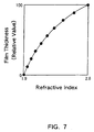
- the variation in refractive index in the transition layer is indicated by a convex curve over the whole region of the transition layer, when the variation is shown on a plane defined by a horizontal axis indicating the refractive index and a vertical axis indicating the thickness direction of the transition layer, with the glass sheet positioned on a lower side.
- the refractive index in the transition layer varies continuously in its thickness direction to approach the refractive index of air (1) from the refractive index of the coating film, in the direction of the outside air.
- the refractive index in the transition layer approaches the refractive index of the another thin film while varying continuously in its thickness direction.
- the refractive index varies continuously from a refractive index n 1 of the coating film to a refractive index n 2 of the thin film formed thereon so that the variation in refractive index is indicated by a convex locus (curve) over the whole region when being shown on a plane.
- the magnitude correlation between the refractive index n 1 and the refractive index n 2 is not particularly limited.
- the coating film is a crystalline coating film. It also is preferable that the roughness is caused by crystal grains in the crystalline coating film.
- the crystalline coating film may contain amorphous portions regionally, and a film with a crystalline fraction in volume of at least 50% as a whole is taken as corresponding to a "crystalline" film.
- the crystalline coating film contains, as a main component, at least one selected from tin oxide, zinc oxide, indium oxide, and titanium oxide. Particularly, a coating film containing tin oxide as the main component is useful for many purposes.
- the "main component” denotes a component accounting for at least 50 wt.% of the whole amount.
- the coating film is formed on an undercoating film on the glass sheet.
- the undercoating film is a coating film formed by pyrolysis of a material containing halogen, and the coating film has a surface with roughness caused by production of or loss after the production of compound grains of an alkaline component in the glass sheet and the halogen. Utilization of the roughness enables a transition layer having the above-mentioned refractive index distribution to be obtained easily.
- the coating film having a surface with roughness may be a coating film formed by pyrolysis of a material containing halogen, and the coating film formed by pyrolysis may have a surface with roughness caused by production of or loss after the production of compound grains of an alkaline component in the glass sheet and the halogen.
- the coating film having a surface with roughness is not required to be a crystalline coating film.
- the thickness of the transition layer in the coating film corresponds to 30% or lower of the thickness of a layer having a substantially constant refractive index in the coating film.
- the thickness of the transition layer is not particularly limited,but preferably corresponds to at least 10% of the thickness of the layer having a substantially constant refractive index in the coating film.
- the coating film having a surface with roughness may be an insulating coating film, but a conductive coating film (a transparent conductive film) is used in a photoelectric conversion device or the like.
- the transparent layered product can be used for various purposes. For example, it can be used as reflection-suppression (anti-reflection) glass, electromagnetic shielding glass, glass to be electrified for preventing fogging or the like, antifouling glass, antistatic glass, low-emissivity glass (Low-E glass), glass for information display equipment (for instance, a touch control panel), or glass for a top plate of a duplicator.
- reflection-suppression (anti-reflection) glass electromagnetic shielding glass
- glass to be electrified for preventing fogging or the like antifouling glass, antistatic glass, low-emissivity glass (Low-E glass), glass for information display equipment (for instance, a touch control panel), or glass for a top plate of a duplicator.
- Low-E glass low-emissivity glass
- glass for information display equipment for instance, a touch control panel
- a top plate of a duplicator for a top plate of a duplicator.
- the transparent layered product may be used as a glass article by being combined with other members.
- the present invention includes a multiple-glazing unit in which at least two transparent substrates are positioned to face each other via at least one inner layer selected from a group consisting of an air layer, an inert gas layer, and a low pressure layer and at least one of the transparent substrates is the transparent layered product.
- the multiple-glazing unit may be used for a door of a refrigerator (a refrigerated display case), and the conductive coating film (a coating film having a surface with roughness) included in the multiple-glazing unit is used as a heating element.
- the refrigerator is provided with an electrification device for passing a current in the conductive coating film.
- this information display equipment displays information through the transparent layered product.
- This information display equipment is provided with a display device for displaying information and the conductive film included in the transparent layered product serves as a transparent electrode.
- this duplicator optically reads information to be duplicated through the transparent layered product.
- the transparent layered product is used as a top plate (a document glass on which an original is placed) of the duplicator, and the conductive coating film included in the transparent layered product serves as an antistatic film.
- the transparent layered product also can be used as a substrate for a photoelectric conversion device.
- the photoelectric conversion device includes: a transparent layered product having a glass sheet and a conductive crystalline coating film having a surface with roughness, which is formed on the glass sheet; at least one photoelectric conversion unit; and a back electrode.
- the surface roughness is caused by crystal grains in the crystalline coating film, and the crystalline coating film includes, at its surface, a transition layer in which the refractive index varies continuously in its thickness direction.
- the photoelectric conversion unit and the back electrode are stacked in this order on the crystalline coating film.
- the variation in the refractive index in the transition layer is shown on a plane defined by a horizontal axis indicating the refractive index and a vertical axis indicating the thickness direction of the transition layer, with the glass sheet positioned on a lower side, the variation in the refractive index is indicated by a convex curve over a whole region of the transition layer.
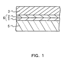
- FIG. 1 is a sectional view of an embodiment of the transparent layered product according to the present invention.
- an undercoating film 6 including a first undercoating layer 1 and a second undercoating layer 2, and a crystalline coating film 3 are formed on a glass sheet 5 in this order.
- the following description is directed to a preferable embodiment when the crystalline coating film 3 is used as a transparent electrode in a photoelectric conversion device.
- a tin oxide film doped with a trace element such as fluorine, antimony, or the like, specifically a fluorine-containing tin oxide film (a SnO 2 :F film) doped with fluorine at a predetermined concentration is preferable.
- the fluorine concentration in the film is 0.15 wt.% or lower.
- This film has a refractive index of about 1.9.
- This crystalline coating film may contain other trace components such as silicon, aluminum, zinc, copper, indium, bismuth, gallium, boron, vanadium, manganese, zirconium, or the like. Preferably, however, the total concentration of such trace components is 0.02 wt.% or lower. It is preferable that the sheet resistance of the crystalline coating film is, specifically, in the range between 5 ⁇ /sq.( ⁇ / ⁇ ) and 25 ⁇ /sq. In view of this sheet resistance, the preferable thickness of the crystalline coating film 3 is in the range between 400 nm and 1200 nm.
- the first undercoating layer 1 has a thickness in the range between 5 nm and 100 nm and a refractive index in the range between 1.6 and 2.5.
- the first undercoating layer 1 is formed of at least one selected from tin oxide, titanium oxide, and aluminum oxide.
- the second undercoating layer 2 has a thickness in the range between 5 nm and 100 nm and a refractive index in the range between 1.4 and 2.0.
- the second undercoating layer 2 is formed of at least one selected from silicon oxide, aluminum oxide, and tin oxide.
- the refractive index of the first undercoating layer is higher than that of the second undercoating layer.
- the structure of the undercoating film 6 is not limited to the two-layer structure, and the undercoating film 6 may be formed of a single layer or three layers or more. A layer in which the refractive index varies continuously may be included between the first undercoating layer and the second undercoating layer. Further, in order to improve plasma resistance, a protective film (for instance, a zinc oxide film) may be formed on the crystalline coating film.
- a protective film for instance, a zinc oxide film
- Layers included in the undercoating film may contain, as a main component, an oxide containing at least two metals such as, for example, silicon-tin oxide (SiSnO).
- Other preferable examples of the layers include a film containing, as a main component, oxycarbide such as for instance silicon oxycarbide (SiOC), or oxynitride.
- oxycarbide film or an oxynitride film in which carbon or nitrogen is introduced has a slightly higher refractive index than that of an oxide film.
- the transparent layered product of the present invention can be used not only for a photoelectric conversion device but also in a wide variety of technical fields.
- the structure, type, and thickness of a coating film are determined suitably depending on the intended use of the transparent layered product.
- the following description is directed to an example of a preferable embodiment when the transparent layered product is used as heat-reflecting glass.
- Heat-reflecting glass may cause harmful light reflection to the surroundings when having an excessively high visible-light reflectance. Therefore, the above-mentioned transparent layered product also is useful as heat-reflecting glass.
- the crystalline coating film 3 is a tin oxide film. To this tin oxide film, other trace components may be added as described above. It is preferable that the crystalline coating film 3 has a thickness in the range between 5 nm and 20 nm. It is preferable that the first undercoating layer 1 has a thickness in the range between 5 nm and 100 nm and a refractive index in the range between 2.5 and 5.0. Preferably, the first undercoating layer 1 is formed of silicon. It is preferable that the second undercoating layer 2 has a thickness in the range between 5 nm and 100 nm and a refractive index in the range between 1.45 and 1.8.
- the second undercoating layer 2 is formed of at least one selected from silicon oxide and aluminum oxide. Further, it is preferable that the refractive index of the first undercoating layer is higher than that of the second undercoating layer.
- the structure of the undercoating film 6 is not limited to the two-layer structure, and the undercoating film 6 may be formed of a single layer or three layers or more.
- transition layer derived from the surface roughness caused by the growth of crystal grains in the crystalline coating film was described.
- the transition layer may be derived from the roughness caused by, in the film, the presence of or the loss after production of a compound of sodium halide or the like produced on the glass sheet surface.
- a coating film is formed by thermally decomposing (pyrolyzing) a material containing chlorine on a glass surface, particularly when the surface temperature of the glass is high, the chlorine and sodium contained in the glass react to produce sodium chloride easily.
- the transition layer in which the variation in refractive index was indicated by a convex curve appeared at the surface of a coating film in which holes formed of the sodium chloride and by the loss of the sodium chloride produced were recognized.
- the transition layer of the crystalline coating film formed on the undercoating film tends to have refractive indexes whose variation is indicated by a convex curve.
- the variation in refractive index per unit thickness is not constant, and typically increases with distance from the glass sheet.
- This variation in refractive index is indicated by a convex curve in a graph over the whole region, when a horizontal axis indicates the refractive index and a vertical axis indicates the thickness direction of the transition layer, with the glass sheet positioned on the lower side.
- a locus of the variation in refractive index can be obtained easily when the crystal grains in the coating film have a dome shape.
- it also has been confirmed that such a locus of the variation in refractive index as described above can be obtained even when the surface has a crater shape obtained by inverting the dome shape.
- the refractive index of the transition layer varies continuously in its thickness direction from the refractive index of the coating film (for example, a refractive index of about 1.9 of tin oxide) to the refractive index of air (1).
- the refractive index in the transition layer varies continuously from the refractive index of the crystalline coating film (for example, about 1.9) to the refractive index of the thin film on the coating film (for instance, a refractive index of about 4.7 of amorphous silicon or a refractive index of about 2.8 of amorphous silicon carbide).
- the thickness of the transition layer corresponds to 30% or less of the thickness of the layer (a nontransition layer) having a substantially constant refractive index in the coating film.
- the thickness of the transition layer corresponds to at least 10 % of that of the nontransition layer.
- the transition layer in which the variation in refractive index is indicated by a convex curve in the graph as described above can have a lower light reflectance than that of a transition layer in which the variation in refractive index is substantially constant.
- One of the methods of manufacturing the transition layer is a pyrolytic method, particularly a CVD method on a glass ribbon in a glass sheet production line by a float glass process.
- the manufacturing method of the transparent layered product according to the present invention is not limited to the CVD method on a glass ribbon. It has not been confirmed that the transition layer is formed without fail when a film is deposited on a glass ribbon, but the CVD method satisfies at least conditions suitable for the formation of the transition layer.
- the transition layer is obtained by the film deposition on a high-temperature glass ribbon by the CVD method has not been confirmed.
- the crystalline nucleus present at the surface of the glass ribbon has an influence on the transition layer.
- the growth of the crystal grains in a crystalline coating film is affected even when the coating film is formed on an undercoating film.
- tin particles adhering to the surface of the glass ribbon in a float bath also contribute to the growth of the crystalline nucleus.
- the transition layer tends to be formed easily.
- thermal energy in forming glass also can be utilized.
- This preferable manufacturing method is particularly suitable for manufacturing a substrate for a photoelectric conversion device or low-emissivity glass, which may be required to be manufactured as a large product for a large window glass, roofing material, or the like.
- the film deposition can be carried out on the surface of glass having a temperature equal to or higher than the softening point.
- the film deposition at a high temperature enables the improvements in film performance, film growth rate, and film deposition reaction efficiency. In addition, defects such as pinholes can be suppressed.
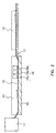
- FIG. 2 shows an embodiment of a device for depositing a film on a glass ribbon in the float glass process by the CVD method.
- a predetermined number of coaters 16 (three coaters 16a, 16b, and 16c in the embodiment shown in the figure) are placed at a predetermined distance from the surface of a glass ribbon 10.
- the glass ribbon 10 is formed from molten glass, which is poured from a furnace 11 into a float bath 12, in a belt-like form on a tin bath 15 while traversing the length of the float bath 12.
- the number and arrangement of the coaters are selected suitably depending on the kind and thickness of a coating film to be formed. These coaters supply gaseous materials to form coating films on the glass ribbon 10 continuously.
- an undercoating film and a crystalline coating film can be formed on the glass ribbon 10 successively by the CVD method.
- the glass ribbon 10 on which the coating films including the crystalline coating film have been formed is lifted by a roller 17 and is carried into an annealing furnace 13.
- the glass ribbon 10 annealed in the annealing furnace 13 is cut by a cutting device, which is not shown in the figure, thus obtaining a glass sheet with a predetermined size.
- Examples of the tin material in the case of using the CVD method include tin tetrachloride, dimethyltin dichloride, dibutyltin dichloride, tetramethyltin, tetrabutyltin, dioctyltin dichloride, monobutyltin trichloride, or the like, and particularly, organic tin chlorides such as dimethyltin dichloride (DMT) and monobutyltin trichloride (MBTC) are preferable.
- Oxidation materials used for obtaining tin oxide from the tin material include oxygen, water vapor, dry air, or the like.
- fluorine material examples include hydrogen fluoride, trifluoroacetic acid, bromotrifluoromethane, chlorodifluoromethane, or the like.
- antimony pentachloride, antimony trichloride, or the like may be used.
- Silicon materials used when a suitable silicon oxide film is deposited as the undercoating film by the CVD method include silane (monosilane), disilane, trisilane, monochlorosilane, dichlorosilane, 1,2-dimethylsilane, 1,1,2-trimethyldisilane, 1,1,2,2-tetramethyl disilane, tetramethyl orthosilicate, tetraethyl orthosilicate, or the like.
- oxidation materials include oxygen, water vapor, dry air, carbon dioxide, carbon monoxide, nitrogen dioxide, ozone, or the like.
- silane for the purpose of preventing the silane from reacting before reaching the glass surface, an unsaturated hydrocarbon gas such as ethylene, acetylene, toluene, or the like may be used also.
- aluminum materials used when a suitable aluminum oxide film is deposited as the undercoating film by the CVD method include trimethylaluminum, aluminum triisopropoxide, diethylaluminum chloride, aluminum acetylacetonate, aluminum chloride, or the like.
- oxygen, water vapor, dry air, or the like can be used as an oxidation material.
- FIG. 4 shows a cross section of an embodiment of a thin film photoelectric conversion device (a thin film silicon-based photoelectric conversion device) using a transparent layered product of the present invention as its substrate.
- a photovoltaic unit 37 is formed and further a back electrode 39 is formed thereon.
- the photovoltaic unit can be formed of a single layer as shown in the figure, but also may be formed by stacking a plurality of layers.
- Examples of the photovoltaic unit include a unit in which an amorphous silicon-based thin film or a crystalline silicon-based thin film is used as a photovoltaic layer (hereinafter the respective units are indicated by referring to the kind of the photovoltaic layer, such as "an amorphous silicon-based thin film photovoltaic unit” and "a crystalline silicon-based thin film photovoltaic unit”).
- An amorphous silicon-based thin film photovoltaic unit can be formed by depositing respective p-type, i-type, and n-type semiconductor layers in this order by a plasma CVD method. Specifically, for example, it may be formed by depositing a p-type microcrystalline silicon-based layer doped with at least 0.01 atom% boron as an impurity atom determining its conductive type, an intrinsic amorphous silicon layer to be a photovoltaic layer, and an n-type microcrystalline silicon-based layer doped with at least 0.01 atom% phosphorus as an impurity atom determining its conductive type in this order.
- these respective layers are not limited to those mentioned above.
- the impurity atom in the p-type microcrystalline silicon-based layer may be aluminum or the like, and an amorphous silicon-based layer may be used as the p-type layer
- an alloy material of amorphous or microcrystalline silicon carbide, silicon germanium, or the like may be used.
- the conductive type (p-type and n-type) silicon-based layers have a thickness in the range between 3 nm and 100 nm, further preferably between 5 nm and 50 nm.
- the intrinsic amorphous silicon layer is formed by the plasma CVD method while the temperature of an undercoating is set to be 450°C or lower.
- This layer is formed as a thin film of substantially an intrinsic semiconductor, with a density of impurity atoms determining its conductive type being limited to 1 ⁇ 10 18 cm -3 or lower. It is preferable that the thickness of the intrinsic amorphous silicon layer is in the range between 0.05 ⁇ m and 0.5 ⁇ m.
- an amorphous silicon carbide layer for instance, an amorphous silicon carbide layer formed of amorphous silicon containing 10 atom% carbon or less
- an amorphous silicon germanium layer for example, an amorphous silicon germanium layer formed of amorphous silicon containing 30 atom% germanium or less
- an alloy material may be formed instead of the intrinsic amorphous silicon layer.
- a crystalline silicon-based thin film photovoltaic unit can be formed by depositing respective p-type, i-type, and n-type semiconductor layers in this order by the plasma CVD method following the same procedure as that used for the amorphous silicon-based thin film photovoltaic unit.
- At least one metallic layer formed of at least one material selected from Al, Ag, Au, Cu, Pt, and Cr is formed by sputtering or vapor deposition.
- a layer formed of conductive oxide such as ITO, SnO 2 , ZnO, or the like may be formed between the photovoltaic unit and the back electrode.
- the photoelectric conversion device of the present invention includes a crystalline silicon-based thin film photovoltaic unit.
- this unit has a lower open circuit voltage and a higher short-circuit current density than those found in an amorphous silicon-based thin film photovoltaic unit, and in this unit, therefore, the light transmittance contributes to the conversion efficiency more than the sheet resistance in the conductive film on the glass sheet does.
- a material with a crystalline fraction in volume of at least 50% is taken as corresponding to a "crystalline" material even if amorphous portions are contained regionally.
- a semiconductor material containing at least 50 atom% silicon for instance, amorphous silicon germanium also is considered as a "silicon-based" material.
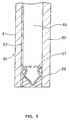
- FIG. 5 is a sectional view showing an embodiment of a double-glazing unit according to the present invention.
- a transparent layered product 60 in which a crystalline coating film 63 is formed on a glass sheet 61 is positioned so that the coating film 63 faces an air layer 66.
- other layers such as an undercoating film or the like may be formed, which is not shown in the figure.
- a conductive coating film is used as the crystalline coating film.
- the peripheries of the transparent layered product 60 and a glass sheet 69 are bonded with a sealant 68 via a spacer 67 containing a desiccant.
- the glass sheet 69 may be a transparent layered product in which a crystalline coating film is formed.
- the air layer 66 may be formed as a low pressure layer by exhausting the inside air to reduce the pressure.
- the pressure inside the air layer 66 is reduced, the insulating effect or the like can be improved further.
- the low pressure layer it is preferable that the peripheries of the transparent layered product and the glass sheet are sealed using, for example, low-melting-point glass instead of using the spacer 67 and the sealant 68. In this case, it is preferred to place a spacer in the low pressure layer to maintain the space between the transparent layered product and the glass sheet.
- an inert gas layer filled with an inert gas such as an argon gas or the like may be used.
- the above-mentioned double-glazing unit can be used as window glass for buildings with an improved thermal insulation property due to the low emissivity of the conductive coating film.
- the double-glazing unit using the transparent layered product also can be used as window glass with an excellent electromagnetic shielding characteristic. Furthermore, it also can be used as glass for a door of a refrigerated display case for shops. When it is used for a door of a refrigerator, the transparent layered product is positioned outside the refrigerator.
- the double-glazing unit shown in the figure is further processed.
- a ground wire is provided for maintaining the conductive coating film to have ground potential.
- an electrode terminal is formed for utilizing the double-glazing unit as a heating element by applying voltage to the conductive coating film, and a wiring is provided for connecting the electrode terminal and a power supply.
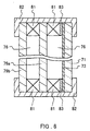
- FIG. 6 is a sectional view of an embodiment of a glass door including a transparent layered product according to the present invention.
- a transparent layered product 71 and glass sheets 79a and 79b are positioned with spaces via air layers 76 and spacers 81, which are combined to form one body using a frame 82, thus forming a multiple-glazing unit.
- a conductive crystalline coating film 73 is formed on the side of the air layer 76.
- electrode terminals 83 are positioned in contact with the coating film 73 at the both ends of the coating film 73.
- This glass door has a function for preventing fogging caused by the heat generation and is suitable as an opening/closing door of a display-type refrigerator used frequently in shops for selling food stuffs or the like.
- respective films including a crystalline coating film were deposited on a glass ribbon using a device for depositing a film as described above.
- the number of coaters was changed suitably depending on the number and thickness of layers to be stacked.
- 98 vol.% nitrogen and 2 vol.% hydrogen were supplied so that the pressure inside the bath was maintained to be slightly higher than that outside the bath, and thus the inside of the bath was maintained under a nonoxidative atmosphere.
- the temperature of the glass ribbon was measured using a pyrometer at a location on a slightly upstream side from the place where the films were formed.
- molten soda-lime silica glass (stained to have a green color) with a flat glass composition was poured into the float bath from a furnace, which then was formed into a glass ribbon with a thickness of 6 mm.
- molten soda-lime silica glass (colorless) with a flat glass composition was poured into the float bath from a furnace, which then was formed into a glass ribbon with a thickness of 3 mm or 4 mm.
- the glass ribbon was annealed in an annealing furnace and then was cut to have a predetermined size on the further downstream side.
- the following comparative examples were obtained by forming transparent layered products having the same film structures as in corresponding examples on a precut glass sheet by the CVD method.
- the glass sheet used in the respective comparative examples had the same thicknesses and compositions as those of the corresponding examples.
- the specific film deposition method will be described as follows.
- a mixed gas containing monosilane and nitrogen was supplied to deposit a silicon film with a thickness of 25 nm on a glass ribbon. Then, from a coater on the downstream side, a mixed gas containing monosilane, ethylene, oxygen, and nitrogen was supplied to deposit a silicon oxide film with a thickness of 20 nm. Subsequently, from a coater on the further downstream side, a mixed gas containing dimethyltin dichloride (vapor), oxygen, water vapor, nitrogen, and helium was supplied to deposit a tin oxide film with a thickness of 12 nm on the silicon oxide film. The temperature of the glass ribbon directly before reaching the coater on the furthest upstream side was 680°C.
- a soda-lime glass sheet with a thickness of 6 mm that had been precut to have a size of 450 mm ⁇ 450 mm was placed on a mesh belt and was passed through a heating furnace to be heated up to about 600°C. While this heated glass sheet was conveyed further, from a coater installed above a glass carrier line, a mixed gas containing monosilane and nitrogen was supplied to deposit a silicon film with a thickness of 25 nm on the glass sheet. This glass sheet was annealed and then was placed on the mesh belt again and was passed through a heating furnace to be heated up to about 600°C.
- Example 1 a silicon film with a thickness of 25 nm, a silicon oxide film with a thickness of 20 nm, and a tin oxide film with a thickness of 12 nm were deposited sequentially on a glass ribbon. After that, from a coater positioned on the further downstream side, a mixed gas containing monosilane, ethylene, oxygen, and nitrogen was supplied to deposit a silicon oxide film with a thickness of 1 nm on the tin oxide film. The temperature of the glass ribbon directly before reaching the coater on the furthest upstream side was 680°C.
- a silicon film with a thickness of 25 nm, a silicon oxide film with a thickness of 20 nm, and a tin oxide film with a thickness of about 12 nm were deposited sequentially on a glass sheet with a thickness of 6 mm. After being annealed, this glass sheet was placed on a mesh belt again and was passed through a heating furnace to be heated up to about 600°C. While this heated glass sheet was conveyed further, from a coater installed above a glass carrier line, a mixed gas containing monosilane, oxygen, and nitrogen was supplied to deposit a silicon oxide film with a thickness of 1 nm on the tin oxide film.
- a mixed gas containing monosilane, ethylene, oxygen, and nitrogen was supplied to deposit a silicon oxide film with a thickness of 40 nm on a glass ribbon.
- a mixed gas containing dimethyltin dichloride (vapor), oxygen, water vapor, nitrogen, helium, and hydrogen fluoride was supplied to deposit a fluorine-containing tin oxide (SnO 2 : F) film with a thickness of 720 nm on the silicon oxide film.
- the temperature of the glass ribbon directly before reaching the coater on the furthest upstream side was 700°C.
- an amorphous silicon carbide layer (a p-type layer) with a thickness of 10 nm was deposited using monosilane, methane, and diborane as raw materials by the plasma CVD method.
- a soda-lime glass sheet with a thickness of 4 mm that had been precut to have a size of 450 mm ⁇ 450 mm was placed on a mesh belt and was passed through a heating furnace to be heated up to about 600°C. While this heated glass sheet was conveyed further, from a coater installed above a glass carrier line, a mixed gas containing monosilane, oxygen, and nitrogen was supplied to deposit a silicon oxide film with a thickness of 25 nm on the glass sheet. After being annealed, this glass sheet was placed on the mesh belt again and was passed through a heating furnace to be heated up to about 600°C.
- an amorphous silicon carbide layer (a p-type layer) with a thickness of 10 nm was deposited using monosilane, methane, and diborane as raw materials by the plasma CVD method.
- a mixed gas containing dimethyltin dichloride (vapor), oxygen, nitrogen, and helium was supplied to deposit a tin oxide film with a thickness of 25 nm on a glass ribbon.
- a mixed gas containing monosilane, ethylene, oxygen, and nitrogen was supplied to deposit a silicon oxide film with a thickness of 15 nm on the tin oxide film.
- a mixed gas containing dimethyltin dichloride (vapor), oxygen, water vapor, nitrogen, helium, and hydrogen fluoride was supplied to deposit a SnO 2 : F film with a thickness of 720 nm on the silicon oxide film.
- the temperature of the glass ribbon directly before reaching the coater on the furthest upstream side was 700°C.
- an amorphous silicon carbide layer (a p-type layer) with a thickness of 10 nm was deposited using monosilane, methane, and diborane as raw materials by the plasma CVD method. Subsequently, an amorphous silicon layer (an i-type layer) with a thickness of 300 nm was stacked using monosilane as a raw material by the same plasma CVD method.
- a soda-lime glass sheet with a thickness of 4 mm that had been precut to have a size of 450 mm ⁇ 450 mm was placed on a mesh belt and was passed through a heating furnace to be heated up to about 600°C. While this heated glass sheet was conveyed further, from a coater installed above a glass carrier line, a mixed gas containing dimethyltin dichloride (vapor), oxygen, nitrogen, and helium was supplied to deposit a tin oxide film with a thickness of 25 nm on the glass sheet. After being annealed, this glass sheet was placed on the mesh belt again and was passed through a heating furnace to be heated up to about 600°C.
- a mixed gas containing dimethyltin dichloride (vapor), oxygen, nitrogen, and helium was supplied to deposit a tin oxide film with a thickness of 25 nm on the glass sheet.
- a mixed gas containing monosilane, oxygen and nitrogen was supplied to deposit a silicon oxide film with a thickness of 15 nm on the tin oxide film.
- the glass sheet was placed on the mesh belt again and was passed through a heating furnace to be heated up to about 600°C.
- a mixed gas containing monobutyltin trichloride (vapor), oxygen, water vapor, nitrogen, and trifluoroacetic acid was supplied to deposit a SnO 2 : F film with a thickness of 720 nm on the silicon oxide film.
- an amorphous silicon carbide layer (a p-type layer) with a thickness of 10 nm was deposited using monosilane, methane, and diborane as raw materials by the plasma CVD method. Subsequently, an amorphous silicon layer (an i-type layer) with a thickness of 300 nm was stacked using monosilane as a raw material by the same plasma CVD method.
- Example 4 As in Example 4, a tin oxide film with a thickness of 25 nm, a silicon oxide film with a thickness of 25 nm, and a SnO 2 : F film with a thickness of 350 nm were deposited sequentially on a glass ribbon.
- the temperature of the glass ribbon directly before reaching the coater on the furthest upstream side was 650°C.
- the above-mentioned thickness of the SnO 2 : F film is in a preferable range for use as low-emissivity glass.
- a tin oxide film with a thickness of 25 nm, a silicon oxide film with a thickness of 25 nm, and a SnO 2 : F film with a thickness of 350 nm were deposited sequentially on a glass sheet.
- Example 4 As in Example 4, a tin oxide film with a thickness of 35 nm, a silicon oxide film with a thickness of 30 nm, and a SnO 2 : F film with a thickness of 520 nm were deposited sequentially on a glass ribbon.
- the temperature of the glass ribbon directly before reaching the coater on the furthest upstream side was 680°C.
- the above-mentioned thickness of the SnO 2 : F film is in a preferable range for use as electromagnetic shielding glass.
- a tin oxide film with a thickness of 35 nm, a silicon oxide film with a thickness of 30 nm, and a SnO 2 : F film with a thickness of 520 nm were deposited sequentially on a glass sheet.
- Example 4 As in Example 4, a tin oxide film with a thickness of 45 nm, a silicon oxide film with a thickness of 40 nm, and a SnO 2 : F film with a thickness of 420 nm were deposited sequentially on a glass ribbon.
- the temperature of the glass ribbon directly before reaching the coater on the furthest upstream side was 680°C.
- the above-mentioned thickness of the SnO 2 : F film is in a preferable range for use as a glass door of a refrigerated display case.
- a tin oxide film with a thickness of 45 nm, a silicon oxide film with a thickness of 40 nm, and a SnO 2 : F film with a thickness of 420 nm were deposited sequentially on a glass sheet.
- Example 4 As in Example 4, a tin oxide film with a thickness of 25 nm, a silicon oxide film with a thickness of 20 nm, and a SnO 2 : F film with a thickness of 270 nm were deposited sequentially on a glass ribbon.
- the temperature of the glass ribbon directly before reaching the coater on the furthest upstream side was 680°C.
- the above-mentioned thickness of the SnO 2 : F film is in a preferable range for use as glass for information display equipment.
- a tin oxide film with a thickness of 25 nm, a silicon oxide film with a thickness of 20 nm, and a SnO 2 : F film with a thickness of 270 nm were deposited sequentially on a glass sheet.
- Example 3 As in Example 3, a silicon oxide film with a thickness of 20 nm and a SnO 2 : F film with a thickness of 40 nm were deposited sequentially on a glass ribbon. The temperature of the glass ribbon directly before reaching the coater on the furthest upstream side was 680°C. The above-mentioned thickness of the SnO 2 : F film is in a preferable range for use as antistatic glass used for a top plate of a duplicator or the like.
- a silicon oxide film with a thickness of 20 nm and a SnO 2 : F film with a thickness of 40 nm were deposited sequentially on a glass sheet.
- a mixed gas containing dimethyltin dichloride (vapor), oxygen, nitrogen, and helium was supplied to deposit a tin oxide film with a thickness of 35 nm on a glass ribbon.
- a mixed gas containing monosilane, ethylene, oxygen, and nitrogen was supplied to deposit a silicon oxide film with a thickness of 25 nm on the tin oxide film.
- a mixed gas containing titanium isopropoxide (vapor), oxygen, water vapor, nitrogen, helium, and trifluoroacetic acid was supplied to deposit a titanium oxide film with a thickness of 250 nm on the silicon oxide film.
- a mixed gas containing monosilane, ethylene, oxygen, and nitrogen was supplied to deposit a silicon oxide film with a thickness of 10 nm on the titanium oxide film.
- the temperature of the glass ribbon directly before reaching the coater on the furthest upstream side was 700°C.
- a soda-lime glass sheet with a thickness of 4 mm that had been precut to have a size of 450 mm ⁇ 450 mm was placed on a mesh belt and was passed through a heating furnace to be heated up to about 600°C. While this heated glass sheet was conveyed further, from a coater installed above a glass carrier line, a mixed gas containing dimethyltin dichloride (vapor), oxygen, nitrogen, and helium was supplied to deposit a tin oxide film with a thickness of 35 nm on the glass sheet. After being annealed, this glass sheet was placed on the mesh belt again and was passed though a heating furnace to be heated up to about 600°C.
- a mixed gas containing dimethyltin dichloride (vapor), oxygen, nitrogen, and helium was supplied to deposit a tin oxide film with a thickness of 35 nm on the glass sheet.
- a mixed gas containing monosilane, oxygen and nitrogen was supplied to deposit a silicon oxide film with a thickness of 25 nm on the tin oxide film.
- the glass sheet was placed on the mesh belt again and was passed through a heating furnace to be heated up to about 600°C.
- a mixed gas containing titanium isopropoxide (vapor), oxygen, water vapor, nitrogen, helium, and trifluoroacetic acid was supplied to deposit a titanium oxide film with a thickness of 250 nm on the silicon oxide film.
- this glass sheet was placed on the mesh belt again and was passed through a heating furnace to be heated up to about 600°C. While this heated glass sheet was conveyed further, from a coater installed above the glass carrier line, a mixed gas containing monosilane, oxygen, and nitrogen was supplied to deposit a silicon oxide film with a thickness of 10 nm on the titanium oxide film.
- a mixed gas containing titanium isopropoxide (vapor), tetraethoxysilane (vapor), oxygen, water vapor, nitrogen, helium, and trifluoroacetic acid was supplied to deposit a titanium-silicon oxide film with a thickness of 130 nm on a glass ribbon.
- a mixed gas containing monosilane, ethylene, oxygen, and nitrogen was supplied to deposit a silicon oxide film with a thickness of 90 nm on the titanium-silicon oxide film.
- the temperature of the glass ribbon directly before reaching the coater on the furthest upstream side was 700°C.
- a soda-lime glass sheet with a thickness of 3 mm that had been precut to have a size of 450 mm ⁇ 450 mm was placed on a mesh belt and was passed through a heating furnace to be heated up to about 600°C. While this heated glass sheet was conveyed further, from a coater installed above a glass carrier line, a mixed gas containing titanium isopropoxide (vapor), tetraethoxysilane (vapor), oxygen, water vapor, nitrogen, helium, and trifluoroacetic acid was supplied to deposit a titanium-silicon oxide film with a thickness of 130 nm on the glass sheet.
- a mixed gas containing titanium isopropoxide (vapor), tetraethoxysilane (vapor), oxygen, water vapor, nitrogen, helium, and trifluoroacetic acid was supplied to deposit a titanium-silicon oxide film with a thickness of 130 nm on the glass sheet.
- this glass sheet was placed on the mesh belt again and was passed through a heating furnace to be heated up to about 600°C. While this heated glass sheet was conveyed further, from a coater installed above the glass carrier line, a mixed gas containing monosilane, oxygen and nitrogen was supplied to deposit a silicon oxide film with a thickness of 90 nm on the titanium-silicon oxide film.
- a mixed gas containing SiH 2 Cl 2 , ethylene, oxygen, and nitrogen was supplied to deposit a silicon oxide film with a thickness of 100 nm on a glass ribbon.
- the temperature of the glass ribbon directly before reaching the coater on the furthest upstream side was 710°C.
- a soda-lime glass sheet with a thickness of 3 mm that had been precut to have a size of 450 mm ⁇ 450 mm was placed on a mesh belt and was passed through a heating furnace to be heated up to about 600°C. While this heated glass sheet was conveyed further, from a coater installed above a glass carrier line, a mixed gas containing SiH 2 Cl 2 , ethylene, oxygen, and nitrogen was supplied to deposit a silicon oxide film with a thickness of 100 nm on the glass sheet.
- the coating film obtained according to Example 12 was observed by an electron microscope.
- sodium chloride was contained and many holes also were confirmed, which seemed to be produced due to the dissociation of the sodium chloride. It is surmised that the sodium chloride was produced by the reaction between sodium in the glass and chlorine in the mixed gas.
- neither sodium chloride nor holes were found. It is conceivable that the use of a material containing chlorine and a high film formation temperature are required for the production of sodium chloride. It was confirmed that the silicon oxide film was a substantially amorphous film.
- a mixed gas containing monosilane and nitrogen was supplied to deposit a silicon film with a thickness of 30 nm on a glass ribbon. Then, from a coater on the downstream side, a mixed gas containing monosilane, ethylene, oxygen, and nitrogen was supplied to deposit a silicon oxide film with a thickness of 50 nm on the silicon film. Subsequently, from a coater on the further downstream side, a mixed gas containing dimethyltin dichloride (vapor), oxygen, water vapor, nitrogen, and helium was supplied to deposit a tin oxide film with a thickness of about 90 nm on the silicon oxide film. The temperature of the glass ribbon directly before reaching the coater on the furthest upstream side was 680°C.
- a soda-lime glass sheet with a thickness of 3 mm that had been precut to have a size of 450 mm ⁇ 450 mm was placed on a mesh belt and was passed through a heating furnace to be heated up to about 600°C. While this heated glass sheet was conveyed further, from a coater installed above a glass carrier line, a mixed gas containing monosilane and nitrogen was supplied to deposit a silicon film with a thickness of 30 nm on the glass sheet. After being annealed, this glass sheet was placed on the mesh belt again and was passed through a heating furnace to be heated up to about 600°C.
- the reflectances and transmittances of samples obtained according to the above-mentioned examples and comparative examples were measured by a spectrophotometer, thus obtaining visible-light reflectances and visible-light transmittances. Furthermore, with respect to respective thin films, corresponding single-layer films with a smooth surface were produced, and the wavelength distribution of the refractive index and extinction coefficient of respective single-layer films was determined by measurement using a spectral ellipsometer, which was used for the following optical calculation.
- the thicknesses of respective transition layers were measured by an interatomic force microscope to obtain rough values. After that, the following optical calculation was carried out using the thickness of each transition layer as a parameter, thus specifying the thickness of each transition layer over a larger area.
- the transition layer was divided in the direction of its thickness (t 2 - t 1 : the principal plane of the glass sheet was set to be 0) and the variation in refractive index (n 1 - n 2 : wherein n 1 denotes the refractive index of a medium (a thin film or air) on the coating film, and n 2 indicates the refractive index of the coating film) was allocated to the respective divided portions.
- the transition layer was divided into at least eight portions in its thickness direction to carry out the allocation.
- the refractive index distribution in the transition layer in each example was able to be better approximated to a model 22. From this, it is conceivable that the actual refractive index distribution of each example is indicated by a curved line such as a curved line 23. This curved line has a convex shape as a whole and no point of inflection. On the other hand, the refractive index distribution assumed from the model most approximated from the results of the respective comparative examples was indicated by a straight line 21 pattern.
- the minimum value of (t p - t q ) / (t 2 - t 1 ) was at least 0.05.
- Tables 1 and 2 show the visible-light reflectance and the visible-light transmittance measured with respect to the respective examples and comparative examples, and the pattern of the variation in refractive index in each transition layer obtained by the above-mentioned calculation.
- the ratio of the transition layer (to a nontransition layer in the coating film in which the transition layer is included) specified by the above was within a range between 10% and 30%.
- FIGs. 7 and 8 show the variations in refractive index of the transition layers in Example 3 and Comparative Example 3, respectively. Visible-Light Reflectance (%) Visible-Light Transmittance (%) Refractive Index Distribution Example 1 41.7 31.9 Convex Curve Comparative Example 1 42.1 31.5 Straight Line Example 2 41.4 32.2 Convex Curve Comparative Example 2 42.2 31.4 Straight Line Example 3 24.9 67.4 Convex Curve Comparative Example 3 25.1 66.8 Straight Line Example 4 10.9 - Convex Curve Comparative Example 4 11.1 - Straight Line Example 5 10.3 85.4 Convex Curve Comparative Example 5 11.1 84.5 Straight Line Example 6 12.4 83.2 Convex Curve Comparative Example 6 13.2 82.4 Straight Line Visible-Light Reflectance (%) Visible-Light Transmittance(%) Refractive Index Distribution Example 7 11.9 84.4 Convex Curve Comparative Example 7 12.4 83.8 Straight Line Example 8 9.6 85.8 Convex Curve Comparative Example 8 10.1 86.4 Straight Line Example 9 9.
- Example 4 As shown in Tables 1 and 2, the respective cases were compared to the corresponding cases using the same film structures, and it was confirmed that the decrease in reflectance and the increase in transmittance in the respective examples with the refractive index distribution indicated by a convex curve were confirmed when compared to those in the comparative examples with the refractive index distribution indicated by a straight line.
- Example 4 and Comparative Example 4 absorption by the amorphous silicon layers was too great to measure the visible-light transmittance.
- the spectral reflectance curves were determined.
- the curve at the beginning on the short wavelength side in the visible region in the example was more gentle than that in the comparative example.
- Such flattening in the reflectance curve was preferable for avoiding the coloring of reflected light, and also results in the decrease in angular dependence of the reflected light color. In a preferable embodiment of the present invention, such preferable effects also can be obtained.
- an amorphous silicon photovoltaic unit was formed by the plasma CVD method, thus obtaining a thin film photoelectric conversion device.
- a p-type amorphous silicon carbide layer and an n-type amorphous silicon layer were used and had thicknesses of 15 nm and 30 nm, respectively.
- An intrinsic amorphous silicon layer (i-type) was formed by a RF plasma CVD method.
- a reaction gas of silane As film deposition conditions, a reaction gas of silane, a pressure inside a reaction chamber of about 40 Pa, a RF power density of 15 mW/cm 2 , and a film deposition temperature of 150°C were used.
- an ITO film with a thickness of 80 nm and an Ag film with a thickness of 300 nm were deposited on the amorphous silicon photovoltaic unit by sputtering in this order.
- the output characteristics of the thin film photoelectric conversion device (with a photovoltaic area of 1 cm 2 ) thus produced were measured while light of AM1.5 (100mW/cm 2 ) was irradiated as incident light.
- the results included an open circuit voltage of 0.89V, a short-circuit current density of 16.4 mA/cm 2 , a fill factor of 72.0%, and a conversion efficiency of 10.5 %.
- an optical degradation test was carried out by irradiating light of AM1.5 (100mW/cm 2 ) at 48°C. After 550 hours irradiation, the conversion efficiency was deteriorated up to 8.7%.
- a transparent layered product with a light reflectance decreased by controlling the variation in refractive index in a transition layer can be provided.
- the present invention can exhibit the effects when a film is formed to add various functions.
- the transparent layered product of the present invention can be used as a glass article including other members. For example, when the transparent layered product is used in a photoelectric conversion device, the conversion efficiency can be improved by reducing the reflection of incident light.
Landscapes
- Chemical & Material Sciences (AREA)
- Life Sciences & Earth Sciences (AREA)
- Engineering & Computer Science (AREA)
- Chemical Kinetics & Catalysis (AREA)
- General Chemical & Material Sciences (AREA)
- Geochemistry & Mineralogy (AREA)
- Materials Engineering (AREA)
- Organic Chemistry (AREA)
- Dispersion Chemistry (AREA)
- Composite Materials (AREA)
- Surface Treatment Of Glass (AREA)
- Special Wing (AREA)
- Laminated Bodies (AREA)
- Joining Of Glass To Other Materials (AREA)
- Chemical Vapour Deposition (AREA)
- Securing Of Glass Panes Or The Like (AREA)
- Photovoltaic Devices (AREA)
- Non-Insulated Conductors (AREA)
Applications Claiming Priority (4)
| Application Number | Priority Date | Filing Date | Title |
|---|---|---|---|
| JP15297299 | 1999-05-31 | ||
| JP15297299 | 1999-05-31 | ||
| JP2000080963 | 2000-03-22 | ||
| JP2000080963A JP4430194B2 (ja) | 1999-05-31 | 2000-03-22 | 透明積層体およびこれを用いたガラス物品 |
Publications (1)
| Publication Number | Publication Date |
|---|---|
| EP1057796A1 true EP1057796A1 (fr) | 2000-12-06 |
Family
ID=26481731
Family Applications (1)
| Application Number | Title | Priority Date | Filing Date |
|---|---|---|---|
| EP00111554A Withdrawn EP1057796A1 (fr) | 1999-05-31 | 2000-05-30 | Produit laminé transparent et article en verre l'utilisant |
Country Status (3)
| Country | Link |
|---|---|
| US (1) | US6362414B1 (fr) |
| EP (1) | EP1057796A1 (fr) |
| JP (1) | JP4430194B2 (fr) |
Cited By (9)
| Publication number | Priority date | Publication date | Assignee | Title |
|---|---|---|---|---|
| US6444898B1 (en) * | 1999-06-18 | 2002-09-03 | Nippon Sheet Glass Co., Ltd. | Transparent layered product and glass article using the same |
| US6498380B1 (en) | 1999-06-18 | 2002-12-24 | Nippon Sheet Glass Co., Ltd. | Substrate for photoelectric conversion device, and photoelectric conversion device using the same |
| WO2003064345A1 (fr) * | 2002-01-31 | 2003-08-07 | Nippon Sheet Glass Company, Limited | Procede de production de plaque de verre a film mince et plaque de verre |
| WO2003065461A1 (fr) * | 2002-01-31 | 2003-08-07 | Nippon Sheet Glass Company, Limited | Substrat pour dispositif de conversion photoelectrique |
| WO2003080530A1 (fr) * | 2002-03-26 | 2003-10-02 | Nippon Sheet Glass Company, Limited | Substrat de verre et processus de production de ce substrat |
| WO2003097549A1 (fr) * | 2002-05-14 | 2003-11-27 | Pilkington North America, Inc. | Article en verre à revêtement de protection solaire réfléchissant |
| EP1462541A4 (fr) * | 2001-12-03 | 2008-03-19 | Nippon Sheet Glass Co Ltd | Procede pour former un film mince, substrat comprenant un film electro-conducteur transparent et dispositif de conversion photoelectrique utilisant le substrat |
| US7585567B2 (en) | 2003-06-17 | 2009-09-08 | Nippon Sheet Glass Company, Limited | Transparent conductive substrate, method of manufacturing the same, and photoelectric conversion element |
| WO2020234594A1 (fr) * | 2019-05-20 | 2020-11-26 | Pilkington Group Limited | Procédé de réduction de l'émissivité d'un article en verre revêtu |
Families Citing this family (39)
| Publication number | Priority date | Publication date | Assignee | Title |
|---|---|---|---|---|
| US6612091B1 (en) * | 1998-12-16 | 2003-09-02 | Michael Glover | Architectural building panel |
| US7976916B2 (en) | 1999-05-25 | 2011-07-12 | Saint-Gobain Vitrage | Refrigerated display case having a transparent insulating glazing unit |
| US20020090521A1 (en) * | 2000-09-29 | 2002-07-11 | Tatsuji Nakajima | Silica layers and antireflection film using same |
| JP2002352956A (ja) * | 2001-03-23 | 2002-12-06 | Mitsubishi Chemicals Corp | 薄膜型発光体及びその製造方法 |
| JP2002287906A (ja) * | 2001-03-23 | 2002-10-04 | Mitsubishi Chemicals Corp | タッチパネル |
| US20030062813A1 (en) * | 2001-07-19 | 2003-04-03 | Cording Christopher R. | Energy-free refrigeration door and method for making the same |
| EP1462540B1 (fr) * | 2001-12-03 | 2012-03-07 | Nippon Sheet Glass Company, Limited | Procede de formation d'un film mince. |
| JP3743363B2 (ja) * | 2001-12-13 | 2006-02-08 | ヤマハ株式会社 | 鍵盤楽器の消音装置 |
| JP4260494B2 (ja) * | 2002-02-26 | 2009-04-30 | 株式会社フジクラ | 透明電極用基材の製法、光電変換素子の製法、及び色素増感太陽電池の製法 |
| WO2004102677A1 (fr) * | 2003-05-13 | 2004-11-25 | Asahi Glass Company, Limited | Substrat conducteur transparent pour batterie solaire et procede de production dudit substrat |
| US7165323B2 (en) * | 2003-07-03 | 2007-01-23 | Donnelly Corporation | Method of manufacturing a touch screen |
| US7160578B2 (en) * | 2004-03-10 | 2007-01-09 | Pilkington North America | Method for depositing aluminum oxide coatings on flat glass |
| PL1730087T3 (pl) * | 2004-03-10 | 2008-03-31 | Pilkington North America Inc | Sposób osadzania powłok tlenku glinowego |
| HUE027526T2 (en) * | 2005-04-29 | 2016-11-28 | Agc Glass Europe | Coated substrate and process for producing coated substrate |
| US8354143B2 (en) * | 2005-05-26 | 2013-01-15 | Tpk Touch Solutions Inc. | Capacitive touch screen and method of making same |
| US8277943B2 (en) * | 2005-10-05 | 2012-10-02 | Certainteed Corporation | Thin films with high near-infrared reflectivity deposited on building materials |
| CN101432453B (zh) * | 2006-04-28 | 2011-12-28 | Sri国际公司 | 用于生产固结的和纯化的材料的方法 |
| JP2009205799A (ja) * | 2006-06-06 | 2009-09-10 | Asahi Glass Co Ltd | 透明導電膜およびその製造方法、ならびにその製造に使用されるスパッタリングターゲット |
| US20080026147A1 (en) * | 2006-07-28 | 2008-01-31 | Gulbrandsen Chemicals, Inc. | Method and formulation for depositing a metal-containing coating on a substrate |
| US7821637B1 (en) | 2007-02-22 | 2010-10-26 | J.A. Woollam Co., Inc. | System for controlling intensity of a beam of electromagnetic radiation and method for investigating materials with low specular reflectance and/or are depolarizing |
| US8610690B2 (en) * | 2007-07-27 | 2013-12-17 | Tpk Touch Solutions Inc. | Capacitive sensor and method for manufacturing same |
| JP2009135044A (ja) * | 2007-11-30 | 2009-06-18 | Tdk Corp | 透明導電材料及び透明導電体 |
| US8126694B2 (en) * | 2008-05-02 | 2012-02-28 | Nanometrics Incorporated | Modeling conductive patterns using an effective model |
| JP2009283520A (ja) * | 2008-05-20 | 2009-12-03 | A & A Material Corp | 軽量太陽光発電パネル |
| US8610691B2 (en) | 2008-08-19 | 2013-12-17 | Tpk Touch Solutions Inc. | Resistive touch screen and method for manufacturing same |
| US9213450B2 (en) * | 2008-11-17 | 2015-12-15 | Tpk Touch Solutions Inc. | Touch sensor |
| DE102009015086A1 (de) * | 2009-03-31 | 2010-10-07 | Schott Ag | Transparente Glas- oder Glaskeramikscheibe mit einer Infrarotstrahlung reflektierenden Schicht |
| US8418418B2 (en) | 2009-04-29 | 2013-04-16 | 3Form, Inc. | Architectural panels with organic photovoltaic interlayers and methods of forming the same |
| CN101618952B (zh) * | 2009-07-30 | 2011-08-17 | 杭州蓝星新材料技术有限公司 | 浮法在线生产透明导电膜玻璃的方法 |
| JP5424059B2 (ja) * | 2009-09-15 | 2014-02-26 | 旭硝子株式会社 | 複層ガラス構造体及び保冷ショーケース |
| KR101155890B1 (ko) * | 2009-10-28 | 2012-06-20 | 엘지전자 주식회사 | 태양 전지 및 그 제조 방법 |
| WO2011126709A2 (fr) * | 2010-03-30 | 2011-10-13 | First Solar, Inc. | Couche tampon dopée |
| DE102010028277B4 (de) * | 2010-04-27 | 2013-04-18 | Calyxo Gmbh | Verfahren und Vorrichtung zur Herstellung einer mit einem Halbleitermaterial beschichteten Glasscheibe und nach dem Verfahren erhältliche Solarzelle oder Solarmodul |
| CN102603209A (zh) * | 2011-01-25 | 2012-07-25 | 鸿富锦精密工业(深圳)有限公司 | 镀膜玻璃及其制备方法 |
| KR102075921B1 (ko) * | 2013-04-29 | 2020-02-11 | 엘지디스플레이 주식회사 | 정전기 방지막 및 그 제조방법, 이를 포함하는 표시장치 |
| WO2015152481A1 (fr) * | 2014-04-02 | 2015-10-08 | (주)비엠씨 | Verre en feuille transparent de type film mince à haute dureté, procédé pour le fabriquer, verre conducteur en feuille transparent de type film mince à haute dureté, et écran tactile le comprenant |
| US20200309995A1 (en) * | 2019-03-26 | 2020-10-01 | Facebook Technologies, Llc | Anti-reflective coatings for transparent electroactive transducers |
| US12013350B2 (en) | 2021-05-05 | 2024-06-18 | Onto Innovation Inc. | Effective cell approximation model for logic structures |
| WO2022255201A1 (fr) * | 2021-05-31 | 2022-12-08 | Agc株式会社 | Substrat avec film stratifié |
Citations (8)
| Publication number | Priority date | Publication date | Assignee | Title |
|---|---|---|---|---|
| DE3436618A1 (de) * | 1983-10-05 | 1985-04-25 | Hitachi, Ltd., Tokio/Tokyo | Glasplatte fuer anzeigevorrichtungen und verfahren zu ihrer herstellung |
| EP0309902A2 (fr) * | 1987-09-30 | 1989-04-05 | Ppg Industries, Inc. | Dépôt chimique en phase vapeur d'oxyde d'étain sur du verre flotté dans le bain d'étain |
| JPH04133360A (ja) * | 1990-09-25 | 1992-05-07 | Sanyo Electric Co Ltd | 光起電力装置 |
| EP0597490A1 (fr) * | 1992-11-13 | 1994-05-18 | Central Glass Company, Limited | Film réduisant la réflexion et procédé pour sa formation sur un substrat en verre |
| US5393563A (en) * | 1991-10-29 | 1995-02-28 | Ellis, Jr.; Frank B. | Formation of tin oxide films on glass substrates |
| EP0782975A1 (fr) * | 1996-01-04 | 1997-07-09 | Ppg Industries, Inc. | Réduction du voile dans des revêtements transparants |
| WO1998006675A1 (fr) * | 1996-08-13 | 1998-02-19 | Pilkington Plc | Procede servant a deposer de l'oxyde d'etain et de l'oxyde de titane sur une plaque de verre et verre revetu au moyen de ce procede |
| EP1056136A1 (fr) * | 1999-05-28 | 2000-11-29 | Nippon Sheet Glass Co., Ltd. | Substrat conducteur pour une cellule solaire et son procédé de fabrication |
Family Cites Families (8)
| Publication number | Priority date | Publication date | Assignee | Title |
|---|---|---|---|---|
| US4732621A (en) | 1985-06-17 | 1988-03-22 | Sanyo Electric Co., Ltd. | Method for producing a transparent conductive oxide layer and a photovoltaic device including such a layer |
| JPS61288473A (ja) | 1985-06-17 | 1986-12-18 | Sanyo Electric Co Ltd | 光起電力装置 |
| US4835040A (en) | 1985-10-07 | 1989-05-30 | Libbey-Owens-Ford Co. | Continuous vapor deposition method for producing a coated glass article |
| US4808462A (en) * | 1987-05-22 | 1989-02-28 | Glasstech Solar, Inc. | Solar cell substrate |
| JP2503615B2 (ja) | 1988-12-28 | 1996-06-05 | カシオ計算機株式会社 | 薄膜トランジスタ及びその製造方法 |
| US5254904A (en) | 1991-05-21 | 1993-10-19 | U.S. Philips Corporation | Antireflective coating layer in particular for a cathode ray tube |
| JPH0729402A (ja) | 1993-07-12 | 1995-01-31 | Stanley Electric Co Ltd | プロジェクタ型ヘッドランプ |
| JPH0741337A (ja) | 1993-07-30 | 1995-02-10 | Glaverbel Sa | 光彩防止透明体 |
-
2000
- 2000-03-22 JP JP2000080963A patent/JP4430194B2/ja not_active Expired - Lifetime
- 2000-05-26 US US09/579,929 patent/US6362414B1/en not_active Expired - Lifetime
- 2000-05-30 EP EP00111554A patent/EP1057796A1/fr not_active Withdrawn
Patent Citations (8)
| Publication number | Priority date | Publication date | Assignee | Title |
|---|---|---|---|---|
| DE3436618A1 (de) * | 1983-10-05 | 1985-04-25 | Hitachi, Ltd., Tokio/Tokyo | Glasplatte fuer anzeigevorrichtungen und verfahren zu ihrer herstellung |
| EP0309902A2 (fr) * | 1987-09-30 | 1989-04-05 | Ppg Industries, Inc. | Dépôt chimique en phase vapeur d'oxyde d'étain sur du verre flotté dans le bain d'étain |
| JPH04133360A (ja) * | 1990-09-25 | 1992-05-07 | Sanyo Electric Co Ltd | 光起電力装置 |
| US5393563A (en) * | 1991-10-29 | 1995-02-28 | Ellis, Jr.; Frank B. | Formation of tin oxide films on glass substrates |
| EP0597490A1 (fr) * | 1992-11-13 | 1994-05-18 | Central Glass Company, Limited | Film réduisant la réflexion et procédé pour sa formation sur un substrat en verre |
| EP0782975A1 (fr) * | 1996-01-04 | 1997-07-09 | Ppg Industries, Inc. | Réduction du voile dans des revêtements transparants |
| WO1998006675A1 (fr) * | 1996-08-13 | 1998-02-19 | Pilkington Plc | Procede servant a deposer de l'oxyde d'etain et de l'oxyde de titane sur une plaque de verre et verre revetu au moyen de ce procede |
| EP1056136A1 (fr) * | 1999-05-28 | 2000-11-29 | Nippon Sheet Glass Co., Ltd. | Substrat conducteur pour une cellule solaire et son procédé de fabrication |
Non-Patent Citations (2)
| Title |
|---|
| GLASS TECHNOLOGY., vol. 23, no. 6, December 1982 (1982-12-01), SOCIETY OF GLASS TECHNOLOGY. SHEFFIELD., GB, pages 271 - 276, XP002146566, ISSN: 0017-1050 * |
| PATENT ABSTRACTS OF JAPAN vol. 016, no. 401 (E - 1253) 25 August 1992 (1992-08-25) * |
Cited By (12)
| Publication number | Priority date | Publication date | Assignee | Title |
|---|---|---|---|---|
| US6444898B1 (en) * | 1999-06-18 | 2002-09-03 | Nippon Sheet Glass Co., Ltd. | Transparent layered product and glass article using the same |
| US6498380B1 (en) | 1999-06-18 | 2002-12-24 | Nippon Sheet Glass Co., Ltd. | Substrate for photoelectric conversion device, and photoelectric conversion device using the same |
| EP1462541A4 (fr) * | 2001-12-03 | 2008-03-19 | Nippon Sheet Glass Co Ltd | Procede pour former un film mince, substrat comprenant un film electro-conducteur transparent et dispositif de conversion photoelectrique utilisant le substrat |
| WO2003064345A1 (fr) * | 2002-01-31 | 2003-08-07 | Nippon Sheet Glass Company, Limited | Procede de production de plaque de verre a film mince et plaque de verre |
| WO2003065461A1 (fr) * | 2002-01-31 | 2003-08-07 | Nippon Sheet Glass Company, Limited | Substrat pour dispositif de conversion photoelectrique |
| WO2003080530A1 (fr) * | 2002-03-26 | 2003-10-02 | Nippon Sheet Glass Company, Limited | Substrat de verre et processus de production de ce substrat |
| US7320827B2 (en) | 2002-03-26 | 2008-01-22 | Nippon Sheet Glass Company, Limited | Glass substrate and method of manufacturing the same |
| WO2003097549A1 (fr) * | 2002-05-14 | 2003-11-27 | Pilkington North America, Inc. | Article en verre à revêtement de protection solaire réfléchissant |
| US6733889B2 (en) | 2002-05-14 | 2004-05-11 | Pilkington North America, Inc. | Reflective, solar control coated glass article |
| AU2003220438B2 (en) * | 2002-05-14 | 2008-10-16 | Pilkington North America, Inc. | Reflective, solar control coated glass article |
| US7585567B2 (en) | 2003-06-17 | 2009-09-08 | Nippon Sheet Glass Company, Limited | Transparent conductive substrate, method of manufacturing the same, and photoelectric conversion element |
| WO2020234594A1 (fr) * | 2019-05-20 | 2020-11-26 | Pilkington Group Limited | Procédé de réduction de l'émissivité d'un article en verre revêtu |
Also Published As
| Publication number | Publication date |
|---|---|
| US6362414B1 (en) | 2002-03-26 |
| JP4430194B2 (ja) | 2010-03-10 |
| JP2001048593A (ja) | 2001-02-20 |
Similar Documents
| Publication | Publication Date | Title |
|---|---|---|
| US6362414B1 (en) | Transparent layered product and glass article using the same | |
| US6444898B1 (en) | Transparent layered product and glass article using the same | |
| US6380480B1 (en) | Photoelectric conversion device and substrate for photoelectric conversion device | |
| US6602606B1 (en) | Glass sheet with conductive film, method of manufacturing the same, and photoelectric conversion device using the same | |
| US7883789B2 (en) | Substrate with transparent conductive oxide film, process for its production and photoelectric conversion element | |
| US20040038051A1 (en) | Conductive film, production method therefor, substrate provided with it and photo-electric conversion device | |
| US7846562B2 (en) | Transparent substrate with transparent conductive film, method of manufacturing the same, and photoelectric conversion element including the substrate | |
| EP1056136B1 (fr) | Substrat conducteur pur un dispositif de conversion photoélectrique et son procédé de fabrication | |
| WO2001028949A1 (fr) | Feuille de verre a film d'oxyde metallique, son procede de production et unite a double vitrage l'utilisant | |
| US6498380B1 (en) | Substrate for photoelectric conversion device, and photoelectric conversion device using the same | |
| US8093490B2 (en) | Method for forming thin film, substrate having transparent electroconductive film and photoelectric conversion device using the substrate | |
| JP4467707B2 (ja) | 導電膜付きガラス板とその製造方法、およびこれを用いた光電変換装置 | |
| JP4430193B2 (ja) | 導電膜付きガラス板の製造方法 | |
| JP3984404B2 (ja) | 導電膜付きガラス板とその製造方法、およびこれを用いた光電変換装置 | |
| JP2001060707A (ja) | 光電変換装置 | |
| JP2004362842A (ja) | 透明導電膜付き透明基体、その製造方法、および光電変換素子用基板ならびに光電変換素子 | |
| JP2017001924A (ja) | コーティング膜つきガラス板 | |
| JP4516657B2 (ja) | 光電変換装置用基板とその製造方法、およびこれを用いた光電変換装置 | |
| JP2024083022A (ja) | 積層膜付き基材 | |
| JP2024083021A (ja) | 膜付き基材 | |
| JPWO2000013237A1 (ja) | 光起電力デバイス |
Legal Events
| Date | Code | Title | Description |
|---|---|---|---|
| PUAI | Public reference made under article 153(3) epc to a published international application that has entered the european phase |
Free format text: ORIGINAL CODE: 0009012 |
|
| AK | Designated contracting states |
Kind code of ref document: A1 Designated state(s): DE FR GB |
|
| AX | Request for extension of the european patent |
Free format text: AL;LT;LV;MK;RO;SI |
|
| RAP1 | Party data changed (applicant data changed or rights of an application transferred) |
Owner name: NIPPON SHEET GLASS CO., LTD. Owner name: KANEKA CORPORATION |
|
| 17P | Request for examination filed |
Effective date: 20010514 |
|
| AKX | Designation fees paid |
Free format text: DE FR GB |
|
| 17Q | First examination report despatched |
Effective date: 20020712 |
|
| STAA | Information on the status of an ep patent application or granted ep patent |
Free format text: STATUS: THE APPLICATION IS DEEMED TO BE WITHDRAWN |
|
| 18D | Application deemed to be withdrawn |
Effective date: 20021123 |