EP1059557A1 - Flüssigkristallanzeige - Google Patents
Flüssigkristallanzeige Download PDFInfo
- Publication number
- EP1059557A1 EP1059557A1 EP99959893A EP99959893A EP1059557A1 EP 1059557 A1 EP1059557 A1 EP 1059557A1 EP 99959893 A EP99959893 A EP 99959893A EP 99959893 A EP99959893 A EP 99959893A EP 1059557 A1 EP1059557 A1 EP 1059557A1
- Authority
- EP
- European Patent Office
- Prior art keywords
- liquid crystal
- substrate
- type polarizing
- polarizing film
- reflection
- Prior art date
- Legal status (The legal status is an assumption and is not a legal conclusion. Google has not performed a legal analysis and makes no representation as to the accuracy of the status listed.)
- Withdrawn
Links
Images


Classifications
-
- G—PHYSICS
- G02—OPTICS
- G02F—OPTICAL DEVICES OR ARRANGEMENTS FOR THE CONTROL OF LIGHT BY MODIFICATION OF THE OPTICAL PROPERTIES OF THE MEDIA OF THE ELEMENTS INVOLVED THEREIN; NON-LINEAR OPTICS; FREQUENCY-CHANGING OF LIGHT; OPTICAL LOGIC ELEMENTS; OPTICAL ANALOGUE/DIGITAL CONVERTERS
- G02F1/00—Devices or arrangements for the control of the intensity, colour, phase, polarisation or direction of light arriving from an independent light source, e.g. switching, gating or modulating; Non-linear optics
- G02F1/01—Devices or arrangements for the control of the intensity, colour, phase, polarisation or direction of light arriving from an independent light source, e.g. switching, gating or modulating; Non-linear optics for the control of the intensity, phase, polarisation or colour
- G02F1/13—Devices or arrangements for the control of the intensity, colour, phase, polarisation or direction of light arriving from an independent light source, e.g. switching, gating or modulating; Non-linear optics for the control of the intensity, phase, polarisation or colour based on liquid crystals, e.g. single liquid crystal display cells
- G02F1/133—Constructional arrangements; Operation of liquid crystal cells; Circuit arrangements
- G02F1/1333—Constructional arrangements; Manufacturing methods
- G02F1/1335—Structural association of cells with optical devices, e.g. polarisers or reflectors
-
- G—PHYSICS
- G02—OPTICS
- G02F—OPTICAL DEVICES OR ARRANGEMENTS FOR THE CONTROL OF LIGHT BY MODIFICATION OF THE OPTICAL PROPERTIES OF THE MEDIA OF THE ELEMENTS INVOLVED THEREIN; NON-LINEAR OPTICS; FREQUENCY-CHANGING OF LIGHT; OPTICAL LOGIC ELEMENTS; OPTICAL ANALOGUE/DIGITAL CONVERTERS
- G02F1/00—Devices or arrangements for the control of the intensity, colour, phase, polarisation or direction of light arriving from an independent light source, e.g. switching, gating or modulating; Non-linear optics
- G02F1/01—Devices or arrangements for the control of the intensity, colour, phase, polarisation or direction of light arriving from an independent light source, e.g. switching, gating or modulating; Non-linear optics for the control of the intensity, phase, polarisation or colour
- G02F1/13—Devices or arrangements for the control of the intensity, colour, phase, polarisation or direction of light arriving from an independent light source, e.g. switching, gating or modulating; Non-linear optics for the control of the intensity, phase, polarisation or colour based on liquid crystals, e.g. single liquid crystal display cells
- G02F1/133—Constructional arrangements; Operation of liquid crystal cells; Circuit arrangements
- G02F1/1333—Constructional arrangements; Manufacturing methods
- G02F1/1335—Structural association of cells with optical devices, e.g. polarisers or reflectors
- G02F1/13363—Birefringent elements, e.g. for optical compensation
- G02F1/133634—Birefringent elements, e.g. for optical compensation the refractive index Nz perpendicular to the element surface being different from in-plane refractive indices Nx and Ny, e.g. biaxial or with normal optical axis
-
- G—PHYSICS
- G02—OPTICS
- G02F—OPTICAL DEVICES OR ARRANGEMENTS FOR THE CONTROL OF LIGHT BY MODIFICATION OF THE OPTICAL PROPERTIES OF THE MEDIA OF THE ELEMENTS INVOLVED THEREIN; NON-LINEAR OPTICS; FREQUENCY-CHANGING OF LIGHT; OPTICAL LOGIC ELEMENTS; OPTICAL ANALOGUE/DIGITAL CONVERTERS
- G02F1/00—Devices or arrangements for the control of the intensity, colour, phase, polarisation or direction of light arriving from an independent light source, e.g. switching, gating or modulating; Non-linear optics
- G02F1/01—Devices or arrangements for the control of the intensity, colour, phase, polarisation or direction of light arriving from an independent light source, e.g. switching, gating or modulating; Non-linear optics for the control of the intensity, phase, polarisation or colour
- G02F1/13—Devices or arrangements for the control of the intensity, colour, phase, polarisation or direction of light arriving from an independent light source, e.g. switching, gating or modulating; Non-linear optics for the control of the intensity, phase, polarisation or colour based on liquid crystals, e.g. single liquid crystal display cells
- G02F1/133—Constructional arrangements; Operation of liquid crystal cells; Circuit arrangements
- G02F1/1333—Constructional arrangements; Manufacturing methods
- G02F1/1335—Structural association of cells with optical devices, e.g. polarisers or reflectors
- G02F1/133528—Polarisers
- G02F1/133536—Reflective polarizers
-
- G—PHYSICS
- G02—OPTICS
- G02F—OPTICAL DEVICES OR ARRANGEMENTS FOR THE CONTROL OF LIGHT BY MODIFICATION OF THE OPTICAL PROPERTIES OF THE MEDIA OF THE ELEMENTS INVOLVED THEREIN; NON-LINEAR OPTICS; FREQUENCY-CHANGING OF LIGHT; OPTICAL LOGIC ELEMENTS; OPTICAL ANALOGUE/DIGITAL CONVERTERS
- G02F1/00—Devices or arrangements for the control of the intensity, colour, phase, polarisation or direction of light arriving from an independent light source, e.g. switching, gating or modulating; Non-linear optics
- G02F1/01—Devices or arrangements for the control of the intensity, colour, phase, polarisation or direction of light arriving from an independent light source, e.g. switching, gating or modulating; Non-linear optics for the control of the intensity, phase, polarisation or colour
- G02F1/13—Devices or arrangements for the control of the intensity, colour, phase, polarisation or direction of light arriving from an independent light source, e.g. switching, gating or modulating; Non-linear optics for the control of the intensity, phase, polarisation or colour based on liquid crystals, e.g. single liquid crystal display cells
- G02F1/133—Constructional arrangements; Operation of liquid crystal cells; Circuit arrangements
- G02F1/1333—Constructional arrangements; Manufacturing methods
- G02F1/1335—Structural association of cells with optical devices, e.g. polarisers or reflectors
- G02F1/133528—Polarisers
- G02F1/133545—Dielectric stack polarisers
-
- G—PHYSICS
- G02—OPTICS
- G02F—OPTICAL DEVICES OR ARRANGEMENTS FOR THE CONTROL OF LIGHT BY MODIFICATION OF THE OPTICAL PROPERTIES OF THE MEDIA OF THE ELEMENTS INVOLVED THEREIN; NON-LINEAR OPTICS; FREQUENCY-CHANGING OF LIGHT; OPTICAL LOGIC ELEMENTS; OPTICAL ANALOGUE/DIGITAL CONVERTERS
- G02F1/00—Devices or arrangements for the control of the intensity, colour, phase, polarisation or direction of light arriving from an independent light source, e.g. switching, gating or modulating; Non-linear optics
- G02F1/01—Devices or arrangements for the control of the intensity, colour, phase, polarisation or direction of light arriving from an independent light source, e.g. switching, gating or modulating; Non-linear optics for the control of the intensity, phase, polarisation or colour
- G02F1/13—Devices or arrangements for the control of the intensity, colour, phase, polarisation or direction of light arriving from an independent light source, e.g. switching, gating or modulating; Non-linear optics for the control of the intensity, phase, polarisation or colour based on liquid crystals, e.g. single liquid crystal display cells
- G02F1/133—Constructional arrangements; Operation of liquid crystal cells; Circuit arrangements
- G02F1/1333—Constructional arrangements; Manufacturing methods
- G02F1/1335—Structural association of cells with optical devices, e.g. polarisers or reflectors
- G02F1/1336—Illuminating devices
- G02F1/13362—Illuminating devices providing polarized light, e.g. by converting a polarisation component into another one
-
- G—PHYSICS
- G02—OPTICS
- G02F—OPTICAL DEVICES OR ARRANGEMENTS FOR THE CONTROL OF LIGHT BY MODIFICATION OF THE OPTICAL PROPERTIES OF THE MEDIA OF THE ELEMENTS INVOLVED THEREIN; NON-LINEAR OPTICS; FREQUENCY-CHANGING OF LIGHT; OPTICAL LOGIC ELEMENTS; OPTICAL ANALOGUE/DIGITAL CONVERTERS
- G02F1/00—Devices or arrangements for the control of the intensity, colour, phase, polarisation or direction of light arriving from an independent light source, e.g. switching, gating or modulating; Non-linear optics
- G02F1/01—Devices or arrangements for the control of the intensity, colour, phase, polarisation or direction of light arriving from an independent light source, e.g. switching, gating or modulating; Non-linear optics for the control of the intensity, phase, polarisation or colour
- G02F1/13—Devices or arrangements for the control of the intensity, colour, phase, polarisation or direction of light arriving from an independent light source, e.g. switching, gating or modulating; Non-linear optics for the control of the intensity, phase, polarisation or colour based on liquid crystals, e.g. single liquid crystal display cells
- G02F1/133—Constructional arrangements; Operation of liquid crystal cells; Circuit arrangements
- G02F1/1333—Constructional arrangements; Manufacturing methods
- G02F1/1335—Structural association of cells with optical devices, e.g. polarisers or reflectors
- G02F1/13363—Birefringent elements, e.g. for optical compensation
- G02F1/133638—Waveplates, i.e. plates with a retardation value of lambda/n
-
- G—PHYSICS
- G02—OPTICS
- G02F—OPTICAL DEVICES OR ARRANGEMENTS FOR THE CONTROL OF LIGHT BY MODIFICATION OF THE OPTICAL PROPERTIES OF THE MEDIA OF THE ELEMENTS INVOLVED THEREIN; NON-LINEAR OPTICS; FREQUENCY-CHANGING OF LIGHT; OPTICAL LOGIC ELEMENTS; OPTICAL ANALOGUE/DIGITAL CONVERTERS
- G02F1/00—Devices or arrangements for the control of the intensity, colour, phase, polarisation or direction of light arriving from an independent light source, e.g. switching, gating or modulating; Non-linear optics
- G02F1/01—Devices or arrangements for the control of the intensity, colour, phase, polarisation or direction of light arriving from an independent light source, e.g. switching, gating or modulating; Non-linear optics for the control of the intensity, phase, polarisation or colour
- G02F1/13—Devices or arrangements for the control of the intensity, colour, phase, polarisation or direction of light arriving from an independent light source, e.g. switching, gating or modulating; Non-linear optics for the control of the intensity, phase, polarisation or colour based on liquid crystals, e.g. single liquid crystal display cells
- G02F1/137—Devices or arrangements for the control of the intensity, colour, phase, polarisation or direction of light arriving from an independent light source, e.g. switching, gating or modulating; Non-linear optics for the control of the intensity, phase, polarisation or colour based on liquid crystals, e.g. single liquid crystal display cells characterised by the electro-optical or magneto-optical effect, e.g. field-induced phase transition, orientation effect, guest-host interaction or dynamic scattering
- G02F1/139—Devices or arrangements for the control of the intensity, colour, phase, polarisation or direction of light arriving from an independent light source, e.g. switching, gating or modulating; Non-linear optics for the control of the intensity, phase, polarisation or colour based on liquid crystals, e.g. single liquid crystal display cells characterised by the electro-optical or magneto-optical effect, e.g. field-induced phase transition, orientation effect, guest-host interaction or dynamic scattering based on orientation effects in which the liquid crystal remains transparent
- G02F1/1396—Devices or arrangements for the control of the intensity, colour, phase, polarisation or direction of light arriving from an independent light source, e.g. switching, gating or modulating; Non-linear optics for the control of the intensity, phase, polarisation or colour based on liquid crystals, e.g. single liquid crystal display cells characterised by the electro-optical or magneto-optical effect, e.g. field-induced phase transition, orientation effect, guest-host interaction or dynamic scattering based on orientation effects in which the liquid crystal remains transparent the liquid crystal being selectively controlled between a twisted state and a non-twisted state, e.g. TN-LC cell
- G02F1/1397—Devices or arrangements for the control of the intensity, colour, phase, polarisation or direction of light arriving from an independent light source, e.g. switching, gating or modulating; Non-linear optics for the control of the intensity, phase, polarisation or colour based on liquid crystals, e.g. single liquid crystal display cells characterised by the electro-optical or magneto-optical effect, e.g. field-induced phase transition, orientation effect, guest-host interaction or dynamic scattering based on orientation effects in which the liquid crystal remains transparent the liquid crystal being selectively controlled between a twisted state and a non-twisted state, e.g. TN-LC cell the twist being substantially higher than 90°, e.g. STN-, SBE-, OMI-LC cells
Definitions
- This invention relates to a structure of a liquid crystal display device for displaying character information and image information using a super twisted nematic (STN) liquid crystal cell.
- STN super twisted nematic
- a liquid crystal display device for displaying character information and image information using a liquid crystal cell is used in various electronic devices from small-sized devices such as a timepiece and a portable telephone to large-sized displays for screens of a television, a personal computer, and the like.
- a liquid crystal display panel in which absorption-type polarizing films are disposed on both sides of the liquid crystal cell with a liquid crystal filled between two transparent substrates in such a manner that respective transmission axes thereof make a desired angle, is used.
- a conventional liquid crystal display device using the optical characteristic of the liquid crystal there is a typical one using a twisted nematic (TN) liquid crystal.
- TN twisted nematic
- a polarizing direction of a linearly polarized light which has passed through the absorption-type polarizing film on the incident side is controlled by an optical rotation of the TN liquid crystal, and when the absorption-type polarizing film on the emitting-out- side is disposed to obtain a normally-white mode, character information and image information are indicated in a black display on white that is the background color.
- liquid crystal display device capable of providing variation in display of character information and image information and additionally variation in design is desired.
- liquid crystal display device using the TN liquid crystal it is necessary to use not a liquid crystal display device using the TN liquid crystal but a liquid crystal display device using a super twisted nematic (STN) liquid crystal cell.
- the liquid crystal display device using the STN liquid crystal cell has highly sharp responsivity in transmittance change in response to a change in applied voltage and a large margin in voltage change can be obtained, thereby enabling a high-split display, resulting in increased pixel density within a display screen. Accordingly, a display capacity can be increased and contrast between a display portion and a background portion is also excellent.
- this STN-type liquid crystal display device has a display mode using a birefringence anisotropy of a liquid crystal, even if using a normally-white mode which is excellent in brightness for a monochrome display, a display color of the background portion at which voltage is not applied to the liquid crystal layer is colored due to an elliptically polarized light.
- the display color of the background is not white but a color close to yellowish green, and the display color of the black display portion at which voltage is applied to the liquid crystal layer is bluish black.
- This invention is made in view of such a present state, and its object is to bring a background for a display to an achromatic color without coloring in an STN-type liquid crystal display device having a large display capacity for information and to make a liquid crystal display device which is new in design and fashionable.
- a liquid crystal display device comprises: an STN liquid crystal cell formed by holding nematic liquid crystal, which is aligned at a twist angle of 180° to 270°, between a transparent first substrate and a transparent second substrate having electrodes on respective opposing inner faces; a reflection-type polarizing film provided outside the first substrate of the STN liquid crystal cell; a first retardation film provided between the reflection-type polarizing film and the first substrate; a backlight provided on the opposite side of the reflection-type polarizing film to the first retardation film; an absorption-type polarizing film provided outside the second substrate of the STN liquid crystal cell; and a second retardation film provided between the absorption-type polarizing film and the second substrate.
- the first and second retardation films are retardation films each of which satisfies conditions of nx > nz > ny of the retardation film, where nx is the refractive index in a stretching direction of the retardation film, ny is the refractive index in a direction orthogonal to the stretching direction, and nz is the refractive index in a thickness direction.
- the absorption-type polarizing film and the reflection-type polarizing film are arranged in such a manner that respective transmission axes are orthogonal to each other.
- a non-reflection layer is provided on the opposite side of the absorption-type polarizing film to the second retardation film or the twisted retardation film.
- the thickness of the above-described first substrate of the STN liquid crystal cell is 0.1 mm to 0.5 mm.
- liquid crystal display device structure as above, a background portion that is a no-voltage-applied portion is brought to a metallic display.
- an amount of light reflected by the reflection-type polarizing film is increased as much as possible so as to bring the no-voltage-applied portion to a bright achromatic metallic display, and that the STN liquid crystal cell is optimized so as to increase the transmittance of a voltage-applied portion within a wide range of wavelength.
- a so-called Z-type retardation film not an ordinary uniaxial-stretching-type, satisfying conditions of nx > nz > ny, where nx is the refractive index in a stretching direction, ny is the refractive index in a direction orthogonal to the stretching direction, and nz is the refractive index in a thickness direction is used for the retardation film, whereby the viewing angle characteristic is improved and incident light from the surroundings is effectively utilized, and thus a brighter display can be obtained.
- a metallic tone characteristic with high reflectance and an excellent transmission characteristic can be obtained and the visibility is improved within a wide viewing angle, so that a liquid crystal display in a bright achromatic metallic display can be realized.
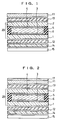
- FIG. 1 and FIG. 2 are schematic sectional views for explaining components of the liquid crystal display device, which is shown with a ratio of a dimension in a direction of thickness being substantially enlarged.
- the liquid crystal display device of the first embodiment is a transflective liquid crystal display device, in which a first substrate 1 and a second substrate 2, each of which is made of a glass plate with a thickness of 0.5 mm, are bonded together with a sealant 5 with a fixed gap therebetween, and nematic liquid crystal 6 which is aligned at a twist angle of 225° is sealed and sandwiched in the gap, thereby forming an STN liquid crystal cell 20 as shown in FIG. 1 and FIG. 2.
- first electrodes 3 made of indium tin oxide (ITO), which is transparent conductive film, are formed, and also on the inner surface of the second substrate 2, second electrodes 4 made of ITO are formed.
- ITO indium tin oxide
- an electro-luminescent (EL) device for the backlight 15, an electro-luminescent (EL) device, a light emitting diode (LED), a cold-cathode tube, a hot-cathode tube, or the like can be used. Further, it is preferable to apply pigments of a fluorescent color to a light-emitting face of the backlight 15 by printing to thereby generate a fluorescent color.
- the upper side is the visible side by an observer and an external light falls from the upper side.
- the ordinary absorption-type polarizing film 11 is a member in a sheet form which has a transmission axis and an absorption axis which are orthogonal to each other, transmits a linearly polarized light polarized in the direction parallel to the transmission axis, and absorbs a linearly polarized light polarized in the direction parallel to the absorption axis.
- the reflection-type polarizing film 14 is a member in a sheet form which has a transmission axis and a reflection axis which are orthogonal to each other, transmits a linearly polarized light polarized in the direction parallel to the transmission axis, and reflects a linearly polarized light polarized in the direction parallel to the reflection axis.
- the arrangement of the backlight 15 which generates a fluorescent color outside the reflection-type polarizing film 14 provides a display in a fluorescent color when a linearly polarized light polarized in the direction parallel to the transmission axis is incident, and when a linearly polarized light polarized in the direction parallel to the reflection axis is made incident, directly reflects the light, thereby obtaining a bright display in a metallic tone because reflection efficiency thereof is high by virtue of a surface in a mirror face state.
- an optical film DBEF (trade name) manufactured by Sumitomo 3M Ltd. is used as the reflection-type polarizing film 14.
- This reflection-type polarizing film is formed with multi-layered thin films with different refractive indices.
- a polarizing film composed of a cholesteric liquid crystal polymer sandwiched between ⁇ /4 (quarter wavelength) films or one utilizing a hologram is applicable.
- Each of the first retardation film 12 and the second retardation film 13 is a film with a thickness of about 70 ⁇ m made of stretched polycarbonate, a so-called Z-type retardation film satisfying conditions of nx > nz > ny, where nx is the refractive index in a stretching direction, fly is the refractive index in a direction orthogonal to the stretching direction, and nz is the refractive index in a thickness direction.
- first retardation film 12 and the reflection-type polarizing film 14, and the second retardation film 13 and the absorption-type polarizing film 11 are respectively bonded together with an acrylic adhesive to be integrated.
- the Z-type retardation film has little change in retardation when seen from a tilted viewing angle, and consequently the viewing angle characteristic of the liquid crystal display device can be improved.
- a light incident on the STN liquid crystal cell 20 from the front passes through the absorption-type polarizing film 11, the second retardation film 13, the second substrate 2, and the liquid crystal 6, further passes through the first substrate 1 and the first retardation film 12, and then reflected at the reflection-type polarizing film 14, passing through the same way as that of the incident light to reach the observer's side as an emitting-out light.
- a liquid crystal layer which an incident in a slanting direction has passed through when it is incident differs from a liquid crystal layer which the light passes through when it is emitted out, whereby a double image in which a display portion appears blurry occurs, resulting in a decrease in display quality.
- the thinner the first substrate 1 is, the more the double image by the incident light in the slanting direction decreases, resulting in an increase in visibility of display.
- the first substrate 1 When the first substrate 1 was prototyped using substrates having various thicknesses, an excellent display quality was obtained in a case of a thickness of 0.5 mm or less.
- a glass plate having a thickness of 0.5 mm is used as both the first substrate 1 and the second substrate 2. It is preferable, however, to thin the first substrate in thickness within 0.1 mm to 0.5 mm.
- the transmittances of the first electrodes 3 and the second electrodes 4 made of ITO are important in terms of brightness and color tone, and thus ITO with high transmittance is required.
- the first electrodes 3 are applied a data signal, which is low in voltage, and thus have little influence due to cross-talk, ITO film with a thickness of 40 nm having a sheet resistance of 100 ohms can be used for them.
- the average transmittance of the first electrodes in that case is about 92%.
- the second electrodes 4 are applied a scanning signal which is high in voltage
- ITO film with a thickness of 230 nm having a sheet resistance of 10 ohms is used for them in order to reduce cross-talk, and thus the average transmittance lowers to about 89%, but the brightness can be improved by employing transparent electrodes having a transmittance of 90% or more at least for the electrodes on one substrate as in this embodiment.
- a non-reflection layer 17 is provided on the surface of the opposite side (the visible side) of the absorption-type polarizing film 11 to the second retardation film 13.
- the non-reflection layer 17 is made by evaporation of inorganic thin film in several layers and a reflectance thereof is about 0.5%.
- the provision of the non-reflection layer 17 causes a reduction of the surface reflection by the absorption-type polarizing film 11, so that the transmittance is improved, resulting in a bright display. Moreover, the emitting-out light to the observer's side is scattered by the non-reflection layer 17, so that a soft color tone in a bright achromatic metallic tone can be obtained.
- a coating-type non-reflection film in which one to two layers of an organic material are applied has been developed recently and has a reflectance of about 1%, which is a little high, but it is low cost.
- Such a non-reflection film can also be used as the non-reflection layer 17 in this embodiment.
- FIG. 3 On the surfaces of the first electrodes 3 and the second electrodes 4, alignment layers (not shown) are respectively formed.
- the inner face of the first substrate 1 is subjected to a rubbing treatment at a 22.5° angle in a counterclockwise direction with respect to a horizontal axis, whereby a lower molecular alignment direction 6a of the liquid crystal 6 is disposed at a +22.5° angle ("+" represents a counterclockwise direction).
- the inner face of the second substrate 2 is subjected to a rubbing treatment at a 22.5° angle in a clockwise direction with respect to the horizontal axis, whereby an upper molecular alignment direction 6b of the liquid crystal 6 is disposed at a -22.5° angle ("-" represents a clockwise direction).
- a so-called "chiral" substance which is an optical rotatory material is added to the nematic liquid crystal 6 having a viscosity of 20cp, and the twisting pitch P thereof is adjusted to 11 ⁇ m, thus forming the STN liquid crystal cell 20 twisted at a 225° angle in a counterclockwise direction.
- a difference ⁇ n in birefringence of the nematic liquid crystal 6 in use is set to be 0.15 and a cell gap d which is a gap between the first substrate 1 and the second substrate 2 is set to be 5.8 ⁇ m.
- a transmission axis 14a of the reflection-type polarizing film 14 is directed at a 0° angle with respect to a horizontal axis
- a transmission axis 11a of the absorption-type polarizing film 11 is directed at a +90° angle with respect to a horizontal axis as shown in FIG. 4
- a stretching axis 12a of the first retardation film 12 is directed at a -70° angle with respect to the horizontal axis as shown in FIG. 3
- a stretching axis 13a of the second retardation film 13 is directed at a +70° angle with respect to the horizontal axis as shown in FIG. 4.
- liquid crystal display device of the first embodiment structured as above in a state where no voltage is applied between the first and second electrodes 3 and 4 of the liquid crystal cell 20, a linearly polarized light reaches the reflection-type polarizing film 14 is all reflected by the reflection-type polarizing film 14 and returned to the visible side, resulting in a bright achromatic, display in a metallic tone like a mirror face.
- Applying voltage between the first electrodes 3 and the second electrodes 4 molecules of the nematic liquid crystal 6 rise and the optical rotation is lost, and thus the linearly polarized light reaches the reflection-type polarizing film 14 passes through it, so that a display color by the color on the surface can be viewed when the backlight 15 is not turned on.
- the display color by a luminescent color of the backlight 15 can be viewed.
- the color on the surface and the luminescent color of the backlight 15 are optionally selected, thereby displaying information in an optional color in a background of a metallic achromatic color, or in contrast to that, displaying information in a metallic achromatic color in a background of an optional color can be realized.
- the Z-type retardation films satisfying conditions of nx > nz > ny are used as the first retardation film 12 and the second retardation film 13, thereby improving the viewing angle characteristic.
- the improvement of the viewing angle characteristic allows light to fall from in various directions, and consequently, the metallic display becomes bright and a liquid crystal display device which is more excellent in visibility can be obtained.
- the similar metallic display can be obtained by optimizing arrangement angles of the absorption-type polarizing film 11, the first retardation film 12, the second retardation film 13, and the reflection-type polarizing film 14.
- the absorption-type polarizing film 11 with a transmittance of 46% is used in this embodiment, it is preferable to use a polarizing film with a transmittance of 45% or more and a polarization degree of 95% or more in order to obtain excellent brightness. It is, of course, possible to use even an absorption-type polarizing film with a transmittance of less than 45%, though the display becomes somewhat dark.
- FIG. 5 and FIG. 6 are schematic sectional views for explaining components of the liquid crystal display device, the same numerals are given to portions corresponding to those in FIG. 1 and FIG. 2, and the description thereof is omitted or simplified.
- the liquid crystal display device of the second embodiment is also a transflective liquid crystal display device and has the same structure as that of the first embodiment except that: a twisted retardation film 16 is disposed in place of the second retardation film 13 in the liquid crystal display device of the first embodiment; the first retardation film 12 is omitted; and the twist angle of the STN liquid crystal cell 20 is different.
- an STN liquid crystal cell 21 is structured similarly to the STN liquid crystal cell 20 of the first embodiment, but nematic liquid crystal 6 which is sealed and sandwiched in a gap between a first substrate 1 and a second substrate 2 is aligned at a twist angle of 240° in a counterclockwise direction.
- a reflection-type polarizing film 14 is disposed, and a backlight 15 is disposed outside the reflection-type polarizing film 14.
- an absorption-type polarizing film 11 with a transmittance of 46% is disposed with the twisted retardation film 16 therebetween.
- the same non-reflection layer 17 as that shown in FIG. 2 is provided on the surface of the opposite side of the absorption-type polarizing film 11 to the twisted retardation film 16.
- the reflection-type polarizing film 14 is the same as that used in the first embodiment.
- first substrate 1, the second substrate 2, first electrodes 3, and second electrodes 4 are the same as those used in the first embodiment, respectively.
- the twisted retardation film 16 is a film that a liquid crystal polymer material having a twist is applied to triacetyl cellulose (TAC) film or polyethylene terephthalate (PET) film after an aligning treatment, brought into a liquid crystal state at a high temperature of about 150°C, and rapidly cooled to room temperature after adjusting the twist angle to fix the twisted state.
- TAC triacetyl cellulose
- PET polyethylene terephthalate
- the non-reflection layer 17 made by evaporation of inorganic thin film in several layers and having a reflectance of about 0.5% is provided on the surface of the absorption-type polarizing film 11, whereby the surface reflection by the absorption-type polarizing film 11 is reduced so that the transmittance is improved, resulting in a bright display. Moreover, the emitting-out light to the visible side is scattered by the non-reflection layer 17, so that a soft color in a bright achromatic metallic tone can be obtained.
- first electrodes 3 and the second electrodes 4 On the surfaces of the first electrodes 3 and the second electrodes 4, alignment layers (not shown) are respectively formed. As shown in FIG. 7, the inner face of the first substrate 1 is subjected to a rubbing treatment at a 30° angle in a clockwise direction with respect to a horizontal axis, whereby a lower molecular alignment direction 6a of the liquid crystal 6 is disposed at a +30° angle. The inner face of the second substrate 2 is subjected to a rubbing treatment at a 30° angle in a counterclockwise direction with respect to the horizontal axis, whereby an upper molecular alignment direction 6b of the liquid crystal 6 is disposed at a -30° angle.
- a so-called "chiral" substance which is an optical rotatory material, is added to the nematic liquid crystal 6 having a viscosity of 20cp and the twisting pitch P thereof is adjusted to 11 ⁇ m, thus forming the STN liquid crystal cell 21 twisted at a left-handed 240° angle.
- a difference ⁇ n in birefringence of the nematic liquid crystal 6 in use is set to be 0.15 and a cell gap d which is a gap between the first substrate 1 and the second substrate 2 is set to be 5.4 ⁇ m.
- ⁇ R 0.005 ⁇ m to 0.05 ⁇ m is preferable.
- a transmission axis 14a of the reflection-type polarizing film 14 is directed at a +75° angle with respect to a horizontal axis as shown in FIG. 7
- a transmission axis 11a of the absorption-type polarizing film 11 is directed at a -15° angle with respect to a horizontal axis as shown in FIG. 8.
- a lower molecular alignment direction 16a of the twisted retardation film 16 is directed at a +60° angle with respect to the horizontal axis
- liquid crystal display device of the second embodiment structured as above in a state where no voltage is applied between the first and second electrodes 3, 4 of the liquid crystal cell 21, a linearly polarized light which reaches the reflection-type polarizing film 14 is all reflected by the reflection-type polarizing film 14 and returned to the visible side, resulting in a bright achromatic display in a metallic tone like a mirror face.
- Applying voltage between the first electrodes 3 and the second electrodes 4 molecules of the nematic liquid crystal 6 rise and the optical rotation is lost, and thus the linearly polarized light which reaches the reflection-type polarizing film 14 passes through it, so that a display color by the color on the surface can be viewed when the backlight 15 is not turned on.
- the display color by a luminescent color of the backlight 15 can be viewed.
- the color on the surface and the luminescent color of the backlight 15 are optionally selected, thereby displaying information in an optional color in a background of a metallic achromatic color, or in contrast to that, displaying information in a metallic achromatic color in a background of an optional color can be realized.
- the viewing angle characteristic is improved, and consequently the metallic display becomes bright and a liquid crystal display device which is more excellent in visibility can be obtained.
- the similar display device can be obtained by optimizing arrangement angles of the absorption-type polarizing film 11, the twisted retardation film 16, and the reflection-type polarizing film 14.
- the absorption-type polarizing film 11 with a transmittance of 46% is used in this embodiment, it is preferable to use a polarizing film with a transmittance of 45% or more and a polarization degree of 95% or more in order to obtain excellent brightness. It is, of course, possible to use even an absorption-type polarizing film with a transmittance of less than 45%, though the display becomes somewhat dark.
- a glass substrate with a thickness of 0.5 mm is used for the first substrate 1, and the thinner the thickness of the first substrate 1 is, the more excellent display quality can be obtained.
- the thickness is preferable in a range from 0.1 mm to 0.5 mm in reality.
- a plastic substrate such as polyethylene terephthalate (PET) may be used for the first and second substrates in place of the glass substrate.
- a liquid crystal display device with a large capacity for information display using an STN liquid crystal cell can be made into a transflective liquid crystal display device capable of displaying information with high brightness and high contrast in an optional color in a background of an achromatic metallic color or an inverse display thereof and which is various in design and fashionable.
- this liquid crystal display device can be applied to display devices such as various kinds of electronic devices as well as a wrist watch, a cellular phone, and a personal digital assistant (PDA), and can be improved in design in appearance and fashion.
- PDA personal digital assistant
Landscapes
- Physics & Mathematics (AREA)
- Nonlinear Science (AREA)
- Mathematical Physics (AREA)
- Chemical & Material Sciences (AREA)
- Crystallography & Structural Chemistry (AREA)
- General Physics & Mathematics (AREA)
- Optics & Photonics (AREA)
- Liquid Crystal (AREA)
- Devices For Indicating Variable Information By Combining Individual Elements (AREA)
Applications Claiming Priority (3)
| Application Number | Priority Date | Filing Date | Title |
|---|---|---|---|
| JP35859398 | 1998-12-17 | ||
| JP35859398 | 1998-12-17 | ||
| PCT/JP1999/007118 WO2000036460A1 (en) | 1998-12-17 | 1999-12-17 | Liquid-crystal display |
Publications (2)
| Publication Number | Publication Date |
|---|---|
| EP1059557A1 true EP1059557A1 (de) | 2000-12-13 |
| EP1059557A4 EP1059557A4 (de) | 2005-04-27 |
Family
ID=18460122
Family Applications (1)
| Application Number | Title | Priority Date | Filing Date |
|---|---|---|---|
| EP99959893A Withdrawn EP1059557A4 (de) | 1998-12-17 | 1999-12-17 | Flüssigkristallanzeige |
Country Status (4)
| Country | Link |
|---|---|
| EP (1) | EP1059557A4 (de) |
| KR (1) | KR100373156B1 (de) |
| CN (1) | CN1291296A (de) |
| WO (1) | WO2000036460A1 (de) |
Cited By (2)
| Publication number | Priority date | Publication date | Assignee | Title |
|---|---|---|---|---|
| US6888596B2 (en) | 2001-09-21 | 2005-05-03 | Hitachi, Ltd. | Liquid crystal display device |
| DE102004022903B4 (de) * | 2003-05-12 | 2007-04-19 | Lg. Philips Lcd Co., Ltd. | Flüssigkristalldisplay |
Families Citing this family (5)
| Publication number | Priority date | Publication date | Assignee | Title |
|---|---|---|---|---|
| WO2006030512A1 (ja) * | 2004-09-16 | 2006-03-23 | Toshiba Matsushita Display Technology Co., Ltd. | 液晶表示素子 |
| US20060114366A1 (en) * | 2004-12-01 | 2006-06-01 | Au Optronics Corporation | Flat-panel display apparatus |
| JP2019095597A (ja) * | 2017-11-22 | 2019-06-20 | スタンレー電気株式会社 | 液晶装置 |
| WO2021130580A1 (en) * | 2019-12-23 | 2021-07-01 | 3M Innovative Properties Company | Optical stack and display |
| EP4016173B1 (de) * | 2020-12-21 | 2024-08-14 | The Swatch Group Research and Development Ltd | Verfahren zur herstellung einer flüssigkristallanzeigevorrichtung und flüssigkristallanzeigevorrichtung |
Family Cites Families (15)
| Publication number | Priority date | Publication date | Assignee | Title |
|---|---|---|---|---|
| US5227903A (en) * | 1991-09-20 | 1993-07-13 | Casio Computer Co., Ltd. | Liquid crystal display device with at least one biaxial retardation film having nx >nz >ny |
| JPH07225372A (ja) * | 1994-02-14 | 1995-08-22 | Hitachi Ltd | 液晶表示装置とその製造方法 |
| JPH0815695A (ja) * | 1994-06-29 | 1996-01-19 | Sony Corp | 液晶表示装置 |
| JPH0862568A (ja) * | 1994-08-19 | 1996-03-08 | Hitachi Ltd | 液晶表示装置 |
| JP3214534B2 (ja) * | 1994-08-29 | 2001-10-02 | アルプス電気株式会社 | カラー液晶表示装置 |
| JPH08114794A (ja) * | 1994-10-14 | 1996-05-07 | Sharp Corp | 液晶表示装置およびその駆動方法 |
| JP3720921B2 (ja) * | 1995-08-02 | 2005-11-30 | 住友化学株式会社 | 液晶表示装置 |
| JP3031842B2 (ja) * | 1995-08-04 | 2000-04-10 | 松下電器産業株式会社 | 液晶表示素子 |
| JP2768319B2 (ja) * | 1995-08-04 | 1998-06-25 | 旭硝子株式会社 | カラー液晶表示素子 |
| JPH09258214A (ja) * | 1996-03-26 | 1997-10-03 | Casio Comput Co Ltd | カラー液晶表示装置 |
| CN1158560C (zh) * | 1996-09-17 | 2004-07-21 | 精工爱普生株式会社 | 显示装置和使用该显示装置的电子装置 |
| US6184955B1 (en) * | 1997-01-17 | 2001-02-06 | Seiko Epson Corporation | Liquid crystal device and electronic apparatus using it |
| US6930738B1 (en) * | 1997-07-30 | 2005-08-16 | Citizen Watch Co., Ltd. | Liquid crystal display with particular reflective switched states |
| US6504588B1 (en) * | 1998-04-28 | 2003-01-07 | Citizen Watch Co., Ltd. | Reflection-type color liquid crystal display device having absorbing member containing fluorescent material |
| EP1014161B1 (de) * | 1998-06-25 | 2001-12-19 | Citizen Watch Co. Ltd. | Reflektierende flüssigkristallanzeige |
-
1999
- 1999-12-17 WO PCT/JP1999/007118 patent/WO2000036460A1/ja not_active Ceased
- 1999-12-17 EP EP99959893A patent/EP1059557A4/de not_active Withdrawn
- 1999-12-17 KR KR10-2000-7007595A patent/KR100373156B1/ko not_active Expired - Fee Related
- 1999-12-17 CN CN99802990A patent/CN1291296A/zh active Pending
Cited By (3)
| Publication number | Priority date | Publication date | Assignee | Title |
|---|---|---|---|---|
| US6888596B2 (en) | 2001-09-21 | 2005-05-03 | Hitachi, Ltd. | Liquid crystal display device |
| US7119871B2 (en) | 2001-09-21 | 2006-10-10 | Hitachi, Ltd. | Liquid crystal display having insulating film overlapping and extending in direction of drain signal line |
| DE102004022903B4 (de) * | 2003-05-12 | 2007-04-19 | Lg. Philips Lcd Co., Ltd. | Flüssigkristalldisplay |
Also Published As
| Publication number | Publication date |
|---|---|
| EP1059557A4 (de) | 2005-04-27 |
| WO2000036460A1 (en) | 2000-06-22 |
| KR20010034001A (ko) | 2001-04-25 |
| CN1291296A (zh) | 2001-04-11 |
| KR100373156B1 (ko) | 2003-02-25 |
Similar Documents
| Publication | Publication Date | Title |
|---|---|---|
| US6717641B2 (en) | Liquid crystal display device | |
| EP1014161B1 (de) | Reflektierende flüssigkristallanzeige | |
| US6504588B1 (en) | Reflection-type color liquid crystal display device having absorbing member containing fluorescent material | |
| KR100846628B1 (ko) | 반투과형 액정표시장치 | |
| EP1152281B1 (de) | Reflektierende lcd, halbdurchlässige reflektierende lcd und elektronische vorrichtung | |
| WO1998048320A1 (en) | Reflection liquid crystal display and reflection liquid crystal display provided with built-in touch panel and comprising the same | |
| US6144432A (en) | Reflective liquid crystal display device | |
| EP1378784A1 (de) | Durchscheinende reflektierende flüssigkristallanzeige | |
| US20050275779A1 (en) | Liquid crystal display | |
| KR100722458B1 (ko) | 액정표시소자 | |
| CN100520519C (zh) | 液晶显示装置和电子设备 | |
| EP1584972B1 (de) | Flüssigkristall-Anzeigenvorrichtung | |
| US6480251B1 (en) | Reflection liquid crystal display element | |
| EP0936490A1 (de) | Flüssigkristall-anzeigevorrichtung | |
| EP1059557A1 (de) | Flüssigkristallanzeige | |
| EP1072928A1 (de) | Reflektierende flüssigkristallanzeigevorrichtung | |
| US6542208B1 (en) | Liquid crystal display device | |
| US7492424B2 (en) | Liquid crystal display device | |
| CN110770642A (zh) | 液晶面板 | |
| JPH04289818A (ja) | 液晶表示装置 | |
| KR100846625B1 (ko) | 반투과형 액정표시장치 | |
| JPWO2000036460A1 (ja) | 液晶表示装置 | |
| JP2004219552A (ja) | 液晶表示装置及び電子機器 | |
| JP2002162619A (ja) | 液晶表示装置 | |
| JPH0432818A (ja) | 液晶表示装置 |
Legal Events
| Date | Code | Title | Description |
|---|---|---|---|
| PUAI | Public reference made under article 153(3) epc to a published international application that has entered the european phase |
Free format text: ORIGINAL CODE: 0009012 |
|
| 17P | Request for examination filed |
Effective date: 20000816 |
|
| AK | Designated contracting states |
Kind code of ref document: A1 Designated state(s): AT BE CH CY DE DK ES FI FR GB GR IE IT LI LU MC NL PT SE |
|
| RAP1 | Party data changed (applicant data changed or rights of an application transferred) |
Owner name: CITIZEN WATCH CO. LTD. |
|
| RBV | Designated contracting states (corrected) |
Designated state(s): DE FR GB NL |
|
| A4 | Supplementary search report drawn up and despatched |
Effective date: 20050311 |
|
| RIC1 | Information provided on ipc code assigned before grant |
Ipc: 7G 02F 1/13363B Ipc: 7G 02F 1/139 B Ipc: 7G 02F 1/1335 A |
|
| STAA | Information on the status of an ep patent application or granted ep patent |
Free format text: STATUS: THE APPLICATION IS DEEMED TO BE WITHDRAWN |
|
| 18D | Application deemed to be withdrawn |
Effective date: 20050527 |