EP1060428B1 - Optische kopplungsvorrichtung zum passiven ausrichten von optoelektronischen bauteilen und lichtleitfasern - Google Patents
Optische kopplungsvorrichtung zum passiven ausrichten von optoelektronischen bauteilen und lichtleitfasern Download PDFInfo
- Publication number
- EP1060428B1 EP1060428B1 EP99909629A EP99909629A EP1060428B1 EP 1060428 B1 EP1060428 B1 EP 1060428B1 EP 99909629 A EP99909629 A EP 99909629A EP 99909629 A EP99909629 A EP 99909629A EP 1060428 B1 EP1060428 B1 EP 1060428B1
- Authority
- EP
- European Patent Office
- Prior art keywords
- optical
- optoelectronic
- optical coupler
- alignment
- holes
- Prior art date
- Legal status (The legal status is an assumption and is not a legal conclusion. Google has not performed a legal analysis and makes no representation as to the accuracy of the status listed.)
- Expired - Lifetime
Links
- 230000003287 optical effect Effects 0.000 title claims description 42
- 230000005693 optoelectronics Effects 0.000 title claims description 36
- 230000008878 coupling Effects 0.000 title claims description 33
- 238000010168 coupling process Methods 0.000 title claims description 33
- 238000005859 coupling reaction Methods 0.000 title claims description 33
- 239000013307 optical fiber Substances 0.000 title claims description 21
- XUIMIQQOPSSXEZ-UHFFFAOYSA-N Silicon Chemical compound [Si] XUIMIQQOPSSXEZ-UHFFFAOYSA-N 0.000 claims description 27
- 229910052710 silicon Inorganic materials 0.000 claims description 27
- 239000010703 silicon Substances 0.000 claims description 27
- 239000000758 substrate Substances 0.000 claims description 11
- 230000013011 mating Effects 0.000 claims description 4
- 230000005540 biological transmission Effects 0.000 claims description 2
- 239000000835 fiber Substances 0.000 description 12
- 238000000034 method Methods 0.000 description 11
- 230000000694 effects Effects 0.000 description 10
- 238000005516 engineering process Methods 0.000 description 9
- 238000001312 dry etching Methods 0.000 description 3
- 239000000463 material Substances 0.000 description 3
- 229920000642 polymer Polymers 0.000 description 3
- 238000001039 wet etching Methods 0.000 description 3
- 230000000295 complement effect Effects 0.000 description 2
- 229910003460 diamond Inorganic materials 0.000 description 2
- 239000010432 diamond Substances 0.000 description 2
- 238000005530 etching Methods 0.000 description 2
- 238000004519 manufacturing process Methods 0.000 description 2
- 238000001020 plasma etching Methods 0.000 description 2
- 229920003295 Radel® Polymers 0.000 description 1
- 229910021417 amorphous silicon Inorganic materials 0.000 description 1
- 239000013078 crystal Substances 0.000 description 1
- 230000001419 dependent effect Effects 0.000 description 1
- 239000004005 microsphere Substances 0.000 description 1
- 229920003023 plastic Polymers 0.000 description 1
- 239000004033 plastic Substances 0.000 description 1
- 239000004417 polycarbonate Substances 0.000 description 1
- 229920000515 polycarbonate Polymers 0.000 description 1
- 239000002861 polymer material Substances 0.000 description 1
- 238000007789 sealing Methods 0.000 description 1
Images


Classifications
-
- G—PHYSICS
- G02—OPTICS
- G02B—OPTICAL ELEMENTS, SYSTEMS OR APPARATUS
- G02B6/00—Light guides; Structural details of arrangements comprising light guides and other optical elements, e.g. couplings
- G02B6/24—Coupling light guides
- G02B6/42—Coupling light guides with opto-electronic elements
- G02B6/4201—Packages, e.g. shape, construction, internal or external details
- G02B6/4246—Bidirectionally operating package structures
-
- G—PHYSICS
- G02—OPTICS
- G02B—OPTICAL ELEMENTS, SYSTEMS OR APPARATUS
- G02B6/00—Light guides; Structural details of arrangements comprising light guides and other optical elements, e.g. couplings
- G02B6/24—Coupling light guides
- G02B6/42—Coupling light guides with opto-electronic elements
- G02B6/4201—Packages, e.g. shape, construction, internal or external details
- G02B6/4219—Mechanical fixtures for holding or positioning the elements relative to each other in the couplings; Alignment methods for the elements, e.g. measuring or observing methods especially used therefor
- G02B6/4228—Passive alignment, i.e. without a detection of the degree of coupling or the position of the elements
- G02B6/423—Passive alignment, i.e. without a detection of the degree of coupling or the position of the elements using guiding surfaces for the alignment
- G02B6/4231—Passive alignment, i.e. without a detection of the degree of coupling or the position of the elements using guiding surfaces for the alignment with intermediate elements, e.g. rods and balls, between the elements
-
- G—PHYSICS
- G02—OPTICS
- G02B—OPTICAL ELEMENTS, SYSTEMS OR APPARATUS
- G02B6/00—Light guides; Structural details of arrangements comprising light guides and other optical elements, e.g. couplings
- G02B6/24—Coupling light guides
- G02B6/42—Coupling light guides with opto-electronic elements
- G02B6/4201—Packages, e.g. shape, construction, internal or external details
- G02B6/4204—Packages, e.g. shape, construction, internal or external details the coupling comprising intermediate optical elements, e.g. lenses, holograms
-
- G—PHYSICS
- G02—OPTICS
- G02B—OPTICAL ELEMENTS, SYSTEMS OR APPARATUS
- G02B6/00—Light guides; Structural details of arrangements comprising light guides and other optical elements, e.g. couplings
- G02B6/24—Coupling light guides
- G02B6/42—Coupling light guides with opto-electronic elements
- G02B6/4201—Packages, e.g. shape, construction, internal or external details
- G02B6/4219—Mechanical fixtures for holding or positioning the elements relative to each other in the couplings; Alignment methods for the elements, e.g. measuring or observing methods especially used therefor
- G02B6/422—Active alignment, i.e. moving the elements in response to the detected degree of coupling or position of the elements
- G02B6/4221—Active alignment, i.e. moving the elements in response to the detected degree of coupling or position of the elements involving a visual detection of the position of the elements, e.g. by using a microscope or a camera
- G02B6/4222—Active alignment, i.e. moving the elements in response to the detected degree of coupling or position of the elements involving a visual detection of the position of the elements, e.g. by using a microscope or a camera by observing back-reflected light
-
- G—PHYSICS
- G02—OPTICS
- G02B—OPTICAL ELEMENTS, SYSTEMS OR APPARATUS
- G02B6/00—Light guides; Structural details of arrangements comprising light guides and other optical elements, e.g. couplings
- G02B6/24—Coupling light guides
- G02B6/42—Coupling light guides with opto-electronic elements
- G02B6/4201—Packages, e.g. shape, construction, internal or external details
- G02B6/4219—Mechanical fixtures for holding or positioning the elements relative to each other in the couplings; Alignment methods for the elements, e.g. measuring or observing methods especially used therefor
- G02B6/422—Active alignment, i.e. moving the elements in response to the detected degree of coupling or position of the elements
- G02B6/4221—Active alignment, i.e. moving the elements in response to the detected degree of coupling or position of the elements involving a visual detection of the position of the elements, e.g. by using a microscope or a camera
- G02B6/4224—Active alignment, i.e. moving the elements in response to the detected degree of coupling or position of the elements involving a visual detection of the position of the elements, e.g. by using a microscope or a camera using visual alignment markings, e.g. index methods
-
- G—PHYSICS
- G02—OPTICS
- G02B—OPTICAL ELEMENTS, SYSTEMS OR APPARATUS
- G02B6/00—Light guides; Structural details of arrangements comprising light guides and other optical elements, e.g. couplings
- G02B6/24—Coupling light guides
- G02B6/42—Coupling light guides with opto-electronic elements
- G02B6/4201—Packages, e.g. shape, construction, internal or external details
- G02B6/4249—Packages, e.g. shape, construction, internal or external details comprising arrays of active devices and fibres
Definitions
- the present invention relates to a device for passively aligning an optical fiber to an optoelectronic device.
- silicon substrates as an optical bench, preferably known as silicon waferboard technology
- silicon waferboard as an optical bench generally utilizes etched features in the silicon waferboard, for example the grooves for holding the optical fiber.
- the silicon waferboard is a monocrystalline material, anisotropic etching is done to create the v grooves for holding the fiber along the surface of the silicon wafer and alignment fiducials used to hold edge emitting optoelectronic devices and effect passive alignment. Further details of anisotropic etching to effect v grooves and alignment fiducials can be found for example in U.S. Patent 4,210,923 to North et al .
- amorphous silicon can be used as the optical bench, with other known techniques such as reactive ion etching (RIE) to effect fiducials utilized for alignment.
- RIE reactive ion etching
- the alignment of an optical fiber to an optoelectronic device in silicon waferboard is most readily effected by the coupling of the fiber to an edge emitting optoelectronic device. This is because of the geometry of the silicon waferboard.
- the fiber is usually held in an etched v groove on the silicon waferboard, and the alignment of the edge emitting optoelectronic device to the fiber relies on precision alignment pedestals on silicon waferboard and the precision notch on the edge emitting optoelectronic device. Thereafter, some type of sealing or covering is required for practical application. This type of technology has been exploited greatly.
- An emerging technology in the optical communications industry is surface emitting and detecting devices.
- VCSBLs vertical cavity surface emitting lasers
- PIN detectors have a photosensitive surface to receive or emit light from or to the top or bottom surface. These devices have certain benefits, and alignment of devices such as these to optical fibers has proved relatively difficult requiring relatively complicated optical structures and paths to effect the coupling.
- Some success has been met in coupling surface emitting and detecting devices through a 90 degree molded optic coupler as is disclosed in U.S. Patents 5,515,468 and 5,708,743 to DeAndrea, et al .
- polymer molded integrated light coupling devices suitable for coupling light from an optical electronic device to an optical fiber and vice versa.
- the polymer molded integrated light coupling device incorporates many functions in a single device. However, the active alignment process of turning the optical electronic device on to maximize coupling while aligning is still required.
- U.S. Patent 5,179,609 to Blonder, et al discloses an example of the use of silicon waferboard to effect coupling between the device and the fiber in a co-linear fashion.
- This reference makes use of two pieces of monocrystalline material as mounting members that have etched therein detents and complementary locations on each of the pieces of the members. These detents receive microspheres to effect alignment of the mounting members to effect the coupling of the device to the fiber.
- the reference Boudreau, et al. discloses an alignment frame for coupling an optical fiber to an optical electronic device with the optical electronic device readily and accurately placed and bonded to the frame by way of alignment pedestals and standoffs. This passive alignment member has certain benefits as are discussed in the application referenced above.
- the invention to Boudreau, et al. is a pigtailed device.
- U.S. Patent 5,539,848 discloses an optoelectronic transceiver including a connector body terminating an optical cable which is aligned with a waveguide by means of connector body pins which engage complementary holes in the waveguide.
- a flexible substrate, on which optoelectronic devices are mounted, is mounted so as to align the optoelectronic devices with light transmitting core regions of the waveguide.
- the flexible substrate provides electrical connection with integrated circuits mounted on other parts of the flexible substrate and a separate substrate on which the transceiver is mounted.
- a further optoelectronic connector is disclosed in U.S. Patent 5,611,013 in which optical fibres of an optical cable terminate in a connector having guide pins which hold the connector in alignment with a body in which embedded or surface mounted optoelectronic devices are mounted.
- the connector does not include any form of light coupling device between the optical fibres and the optoelectronic devices.
- a connectorized device which enables the coupling of an optical fiber to an optical electronic device which is either surface emitting or surface receiving in a passively aligned manner.
- the present invention comprises a combination of an optoelectronic transceiver and a mating connector as set out in claim 1 and concerns a passive alignment scheme for aligning surface emitting/detecting optical ,electronic devices to optical fibers possibly through the use of a mini-MT ferrule used in a RJ connector by way of silicon waferboard technology.
- the mini-MT ferrule has guide pins which are used to align the optical fiber ultimately to the optoelectronic device.
- a light coupling device having holes for receiving the guide pins as well as lens elements for coupling light between the optical fibers and the optical electronic devices is used.
- the light coupling device is positioned between the optical fibers in the ferrule and the optoelectronic devices mounted on the silicon waferboard and has a recess on each end to accurately control the distance between the lenses and the optical electronic devices as well as the distance between the lenses and the optical fibers. Additionally, the distance between the lens and guide pinholes is precisely controlled to properly effect the alignment of the optical fibers to the lenses and ultimately to the optical electronic devices. Silicon waferboard technology is used rather extensively in the invention of the present disclosure as the optical bench for the optical electronic devices. In addition, alignment fiducuals to include x-y alignment pedestals and z-alignment standoffs are also used to accurately locate and precisely align in a passive manner the optical electronic devices of the present invention.
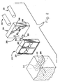
- Figure 1 shows an example of this invention in a MT-RJ transceiver.
- the guide pins 201 provide alignment through silicon wafer board 202, light coupling device 203, and mini-MT ferrule in a RJ connector 204.
- a dry etching with sub-micron accuracy process is used to produce the two circular shaped holes 2,05 for alignment with the guide pins 201 and different shaped pedestals and standoffs 206, 301 for passive alignment with the optoelectronic chips 303, 304 in the x-y and z directions, respectively.
- the dry etching technique is well known to one of ordinary skill in the art.
- the optoelectronic chips have the mating notches, cleaved edges, and/or other alignment fiducials for passive alignment with the silicon wafer board.
- the light coupling device has two holes 209 for alignment with the guide pins 201 and two lenses 207 for collimating the light from the optoelectronic chips to the fiber in the mini-MT ferrule and vice versa. The precise locations of these two lenses with respect to the two holes in this light coupling device provide a very effective method of light coupling between the fibers and the optoelectronic chips.
- the lenses 401 as well as the alignment holes 402 for receiving the pin are shown disposed on the light coupling device 400.
- the light coupling device is fabricated from polymer material, for example Radel (RTM). However, other materials such as polycarbonate or suitable polymers or plastics within the purview of one of ordinary skill in the art can be used to fabricate the light coupling device 400.
- the lenses 401 are molded and are maintained at a precise distance D3 from the center of the guide pins 402 as is shown in top view in figure 5 .
- the light coupling device 400 has a recess on each side shown as 403. The recess is also on the reverse side of the light coupling device. This recess enables a tight control of the distance between the lens 401 and the optical fiber on one side and the distance between the lens and the optical electronic device on the other side.
- the ridge 404 between the lenses 401 is to minimize cross-talk, as it must be remembered that one lens couples light between a fiber and a light emitting device and the other lens couples light between a fiber and a light detecting device.
- the distance between the lenses 207,401 and the opto-electronic devices 303,304 is shown as D1 in Figure 5 and the distance between the lenses 207,401 and the optical fibers 208 is shown as D2 is Figure 5 . Furthermore, again as shown in Figure 5 , the distance between the lenses 401 and the guide pin holes 402 is designated as D3. These distances are controlled with great precision to properly couple the optoelectronic devices and the optical fibers to the lens elements 401. Through the optical coupling device 400, a precise coupling between the fibers 208 (shown in in Figure2 ) is achieved.
- the apparatus shown in Figure 2 is similar to that of Figure 1 , except a wet etching process with sub-micron accuracy is used to produce the two diamond shaped holes 209 in the silicon wafer board with certain crystal orientation.
- the light coupling device is the same in both embodiments.
- the wet etching technique is well known to one of ordinary skill in the art.
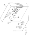
- the mating of the silicon wafer board and the optoelectronic chips 303 is shown in Figure 3 .
- the pedestals and standoffs 301 are schematically shown on the silicon wafer board.
- the notches and/or cleaved edges are shown on the optoelectronic chips.
- the passive alignment fiducials 301 are shown in Figure 3 .
- the holes for the guide pins 302 are for receiving the guide pins 201.
- the devices shown as 303, 304 are the surface emitting/detecting devices of the present disclosure.
- 303 is a PIN detector while the device 304 is a transmitting device, for example VCSEL or a surface emitting LED (SLED).
- the choice of the devices is dependent upon the ultimate use of the device as it is well known to one of ordinary skill in the art that light emitting diodes are for lower speed (transmission rate) operation and lasers are for higher data rate operation.
- the alignment fiducials, pedestals and standoffs provide for x,y and z alignment via the silicon waferboard 300. These alignment fiducuals are fabricated by techniques well known to one of ordinary skill in the art, and can be fabricated by both wet and dry etching techniques.
Landscapes
- Physics & Mathematics (AREA)
- General Physics & Mathematics (AREA)
- Optics & Photonics (AREA)
- Optical Couplings Of Light Guides (AREA)
Claims (6)
- Kombination, die einen optoelektronischen Sender/Empfänger und einen Gegensteckverbinder einschließlich einer Faserendhülse (204) umfasst, die eine Sendelichtleitfaser (208) und eine Empfangslichtleitfaser (208) hat, die in derselben angeordnet sind, wobei der Sender/Empfänger Folgendes umfasst:einen optischen Koppler (203), der angrenzend an die Faserendhülse (204) und in optischer Verbindung mit den Lichtleitfasern (208) angeordnet ist, undein Substrat (202), das eine optoelektronische Oberflächenemitter-Vorrichtung (304) und eine optoelektronische Oberflächendetektor-Vorrichtung (303) hat, die auf demselben angeordnet sind, wobei sich die optoelektronische Oberflächendetektor-Vorrichtung (303) und die optoelektronische Oberflächenemitter-Vorrichtung (304) in optischer Verbindung mit dem optischen Koppler (203) befinden,wobei die Kombination Führungsstifte (201) umfasst, die in selektiv angeordneten Löchern (209) in dem optischen Koppler (203) angeordnet sind, um die Faserendhülse (204) mit dem optischen Koppler (203) auszurichten,
dadurch gekennzeichnet, dass die Führungsstifte (201) ebenfalls in selektiv angeordneten Löchern (205) in dem Substrat (202) angeordnet sind und die Löcher (209) in dem optischen Koppler (203) Durchgangslöcher sind, wodurch sich die gleichen Führungsstifte (201) von den Löchern (205) in dem Substrat (202) durch die Löcher (209) in dem optischen Koppler (203) und in Löcher in der Faserendhülse (204) erstrecken, um eine Ausrichtung zwischen der Faserendhülse (204), dem optischen Koppler (203) und dem Substrat (202) zu gewährleisten. - Kombination nach Anspruch 1, wobei der optische Koppler (203) selektiv angeordnete Linsen (207) hat, um Licht zwischen den Fasern und der optoelektronischen Oberflächendetektor-Vorrichtung (303) und der optoelektronischen Oberflächenemitter-Vorrichtung (304) zu koppeln.
- Kombination nach Anspruch 1 oder 2, wobei das Substrat (202) Silizium ist.
- Kombination nach Anspruch 3, wobei das Siliziumsubstrat selektiv angeordnete X-Y-Ausrichtungssockel und Z-Ausrichtungsabstandsstücke (301) für eine passive Ausrichtung der optoelektronischen Oberflächenemitter-Vorrichtung (304) und der optoelektronischen Oberflächendetektor-Vorrichtung (303) hat.
- Kombination nach einem der vorhergehenden Ansprüche, wobei der optische Koppler (203) einen Übersprech-Minimierungssteg (404) hat, der zwischen Linsen (401) an dem optischen Koppler (400) angeordnet ist.
- Kombination nach einem der vorhergehenden Ansprüche, die ferner eine Aussparung auf jeder Seite des optischen Kopplers (203) umfasst, um die Entfernungen zwischen einer Linse (207) in dem optischen Koppler (203) und erstens den optoelektronischen Vorrichtungen (303, 304) und zweitens den Lichtleitfasern (208) zu steuern.
Applications Claiming Priority (3)
| Application Number | Priority Date | Filing Date | Title |
|---|---|---|---|
| US09/031,585 US5913002A (en) | 1997-12-31 | 1998-02-27 | Optical coupling device for passive alignment of optoelectronic devices and fibers |
| US31585 | 1998-02-27 | ||
| PCT/US1999/004174 WO1999044087A1 (en) | 1998-02-27 | 1999-02-26 | Optical coupling device for passive alignment of optoelectronic devices and optical fibers |
Publications (2)
| Publication Number | Publication Date |
|---|---|
| EP1060428A1 EP1060428A1 (de) | 2000-12-20 |
| EP1060428B1 true EP1060428B1 (de) | 2008-07-02 |
Family
ID=21860301
Family Applications (1)
| Application Number | Title | Priority Date | Filing Date |
|---|---|---|---|
| EP99909629A Expired - Lifetime EP1060428B1 (de) | 1998-02-27 | 1999-02-26 | Optische kopplungsvorrichtung zum passiven ausrichten von optoelektronischen bauteilen und lichtleitfasern |
Country Status (5)
| Country | Link |
|---|---|
| US (1) | US5913002A (de) |
| EP (1) | EP1060428B1 (de) |
| AU (1) | AU2879599A (de) |
| DE (1) | DE69939010D1 (de) |
| WO (1) | WO1999044087A1 (de) |
Families Citing this family (50)
| Publication number | Priority date | Publication date | Assignee | Title |
|---|---|---|---|---|
| US6085007A (en) * | 1998-02-27 | 2000-07-04 | Jiang; Ching-Long | Passive alignment member for vertical surface emitting/detecting device |
| US6249619B1 (en) * | 1998-09-17 | 2001-06-19 | Agere Systems Optoelectronics Guardian Corp. | Optical isolator |
| US20030034438A1 (en) * | 1998-11-25 | 2003-02-20 | Sherrer David W. | Optoelectronic device-optical fiber connector having micromachined pit for passive alignment of the optoelectronic device |
| JP2000196538A (ja) * | 1998-12-25 | 2000-07-14 | Nec Corp | 送受一体型光学系ユニット |
| US6213651B1 (en) | 1999-05-26 | 2001-04-10 | E20 Communications, Inc. | Method and apparatus for vertical board construction of fiber optic transmitters, receivers and transceivers |
| US6901221B1 (en) | 1999-05-27 | 2005-05-31 | Jds Uniphase Corporation | Method and apparatus for improved optical elements for vertical PCB fiber optic modules |
| US6434308B1 (en) * | 1999-09-03 | 2002-08-13 | Teraconnect, Inc | Optoelectronic connector system |
| US6374004B1 (en) * | 1999-10-14 | 2002-04-16 | Digital Optics Corporation | Optical subassembly |
| US6406195B1 (en) | 1999-10-14 | 2002-06-18 | Digital Optics Corporation | Interface between opto-electronic devices and fibers |
| USD446501S1 (en) | 2000-02-07 | 2001-08-14 | Panduit Corp. | Fiber optic transceiver |
| US6540409B1 (en) | 2000-03-09 | 2003-04-01 | Kevin S. Yamada | Apparatus for creating an optical fiber link |
| US6595700B2 (en) * | 2000-04-04 | 2003-07-22 | Shipley Company, L.L.C. | Optoelectronic packages having insulation layers |
| US6726372B1 (en) | 2000-04-06 | 2004-04-27 | Shipley±Company, L.L.C. | 2-Dimensional optical fiber array made from etched sticks having notches |
| US6588942B1 (en) | 2000-04-06 | 2003-07-08 | Fitel Usa Corp. | Optical system having improved fiber-device coupling |
| US6976792B1 (en) | 2000-09-26 | 2005-12-20 | International Business Machines Corporation | Optical fiber space transformation |
| GB2370373A (en) * | 2000-12-22 | 2002-06-26 | Mitel Semiconductor Ab | Alignment of optical assemblies |
| US6634802B2 (en) | 2001-08-09 | 2003-10-21 | International Business Machines Corporation | Optical-electronic array module and method therefore |
| US7110633B1 (en) | 2001-08-13 | 2006-09-19 | Calient Networks, Inc. | Method and apparatus to provide alternative paths for optical protection path switch arrays |
| US7056032B2 (en) * | 2001-09-17 | 2006-06-06 | Stratos International, Inc. | Transceiver assembly for use in fiber optics communications |
| US7073955B1 (en) | 2001-09-17 | 2006-07-11 | Stratos International, Inc. | Transceiver assembly for use in fiber optics communications |
| US7073954B1 (en) | 2001-09-17 | 2006-07-11 | Stratos International, Inc. | Transceiver assembly for use in fiber optics communications |
| US6676302B2 (en) * | 2001-09-17 | 2004-01-13 | Stratos Lightwave, Inc. | Method of constructing a fiber optics communications module |
| US7224856B2 (en) | 2001-10-23 | 2007-05-29 | Digital Optics Corporation | Wafer based optical chassis and associated methods |
| US6866427B2 (en) * | 2001-11-13 | 2005-03-15 | Lumenyte International Corporation | Fiber optic LED light |
| US6643420B2 (en) | 2001-12-28 | 2003-11-04 | Digital Optics Corp. | Optical subassembly |
| US6661955B1 (en) | 2002-02-04 | 2003-12-09 | Siwave, Inc. | Kinematic and non-kinematic passive alignment assemblies and methods of making the same |
| US6850675B1 (en) | 2002-02-04 | 2005-02-01 | Siwave, Inc. | Base, payload and connecting structure and methods of making the same |
| US6674585B1 (en) | 2002-02-04 | 2004-01-06 | Siwave, Inc. | Flexure assemblies and methods of making the same |
| US7813634B2 (en) | 2005-02-28 | 2010-10-12 | Tessera MEMS Technologies, Inc. | Autofocus camera |
| NL1021205C2 (nl) * | 2002-08-02 | 2004-02-18 | Framatome Connectors Int | Optisch connector samenstel, koppelstuk en werkwijze voor het positioneren van het koppelstuk en een structuur van golfgeleiders. |
| US6821028B2 (en) * | 2002-08-30 | 2004-11-23 | Digital Optics Corp. | Optical and mechanical interface between opto-electronic devices and fibers |
| JP3896951B2 (ja) | 2002-11-13 | 2007-03-22 | 松下電器産業株式会社 | 光通信用送受光モジュール |
| CN100539214C (zh) * | 2004-10-29 | 2009-09-09 | 奥斯兰姆奥普托半导体有限责任公司 | 照明装置,汽车车头灯以及照明装置的制造方法 |
| DE102004056252A1 (de) * | 2004-10-29 | 2006-05-04 | Osram Opto Semiconductors Gmbh | Beleuchtungseinrichtung, Kfz-Scheinwerfer und Verfahren zur Herstellung einer Beleuchtungseinrichtung |
| US7334946B2 (en) * | 2005-12-21 | 2008-02-26 | Intel Corporation | Passively aligned optical-electrical interface with microlenses |
| US20090239429A1 (en) | 2007-03-21 | 2009-09-24 | Kipp Michael D | Sound Attenuation Building Material And System |
| US8445101B2 (en) | 2007-03-21 | 2013-05-21 | Ashtech Industries, Llc | Sound attenuation building material and system |
| CA2681528C (en) | 2007-03-21 | 2018-10-23 | Ashtech Industries, Llc | Utility materials incorporating a microparticle matrix |
| WO2010054029A2 (en) | 2008-11-04 | 2010-05-14 | Ashtech Industries, L.L.C. | Utility materials incorporating a microparticle matrix formed with a setting system |
| US9052476B2 (en) * | 2012-07-04 | 2015-06-09 | Sae Magnetics (H.K.) Ltd. | Wafer-level packaged optical subassembly and transceiver module having same |
| US9134490B2 (en) | 2012-12-06 | 2015-09-15 | Laxense Inc. | Passive alignment multichannel parallel optical system |
| US9804334B2 (en) | 2015-10-08 | 2017-10-31 | Teramount Ltd. | Fiber to chip optical coupler |
| US12189195B2 (en) | 2015-10-08 | 2025-01-07 | Teramount Ltd. | Optical coupling |
| US12124087B2 (en) | 2015-10-08 | 2024-10-22 | Teramount Ltd. | Wideband surface coupling |
| US12265259B2 (en) | 2019-01-23 | 2025-04-01 | Teramount Ltd. | Waveguide mode coupling |
| US11585991B2 (en) | 2019-02-28 | 2023-02-21 | Teramount Ltd. | Fiberless co-packaged optics |
| US12379555B2 (en) | 2021-10-27 | 2025-08-05 | Teramount Ltd. | Detachable connector for co-packaged optics |
| US12164159B2 (en) | 2021-12-22 | 2024-12-10 | Teramount Ltd. | Backside optical connector |
| US10564374B2 (en) | 2015-10-08 | 2020-02-18 | Teramount Ltd. | Electro-optical interconnect platform |
| CN110048289B (zh) * | 2019-05-28 | 2020-01-07 | 四川大学 | 连接器信号针安装工具及安装方法 |
Family Cites Families (11)
| Publication number | Priority date | Publication date | Assignee | Title |
|---|---|---|---|---|
| US4210923A (en) * | 1979-01-02 | 1980-07-01 | Bell Telephone Laboratories, Incorporated | Edge illuminated photodetector with optical fiber alignment |
| US5179609A (en) * | 1991-08-30 | 1993-01-12 | At&T Bell Laboratories | Optical assembly including fiber attachment |
| DE69416016T2 (de) * | 1993-02-23 | 1999-07-15 | The Whitaker Corp., Wilmington, Del. | Faseroptische Kopplungseinrichtung |
| US5420954A (en) * | 1993-05-24 | 1995-05-30 | Photonics Research Incorporated | Parallel optical interconnect |
| US5420953A (en) * | 1994-02-17 | 1995-05-30 | The Whitaker Corporation | Optoelectronic integration of holograms using (110) oriented silicon on (100) oriented silicon waferboard |
| SE9402082L (sv) * | 1994-06-14 | 1995-12-15 | Ericsson Telefon Ab L M | Optisk miniatyrkapsel |
| US5539848A (en) * | 1995-05-31 | 1996-07-23 | Motorola | Optical waveguide module and method of making |
| EP1018050B1 (de) * | 1995-06-30 | 2001-12-12 | The Whitaker Corporation | Vorrichtung zur ausrichtung eines optoelektronischen bauteils |
| US5774614A (en) * | 1996-07-16 | 1998-06-30 | Gilliland; Patrick B. | Optoelectronic coupling and method of making same |
| US5842696A (en) * | 1996-07-25 | 1998-12-01 | Moore Business Forms, Inc. | Turn-over and shingling apparatus |
| WO1998014813A1 (en) * | 1996-09-30 | 1998-04-09 | The Whitaker Corporation | Fiber optic array transmitter/receiver based on flexible circuit technology |
-
1998
- 1998-02-27 US US09/031,585 patent/US5913002A/en not_active Expired - Lifetime
-
1999
- 1999-02-26 WO PCT/US1999/004174 patent/WO1999044087A1/en not_active Ceased
- 1999-02-26 AU AU28795/99A patent/AU2879599A/en not_active Abandoned
- 1999-02-26 DE DE69939010T patent/DE69939010D1/de not_active Expired - Fee Related
- 1999-02-26 EP EP99909629A patent/EP1060428B1/de not_active Expired - Lifetime
Also Published As
| Publication number | Publication date |
|---|---|
| US5913002A (en) | 1999-06-15 |
| WO1999044087A1 (en) | 1999-09-02 |
| EP1060428A1 (de) | 2000-12-20 |
| AU2879599A (en) | 1999-09-15 |
| DE69939010D1 (de) | 2008-08-14 |
Similar Documents
| Publication | Publication Date | Title |
|---|---|---|
| US5913002A (en) | Optical coupling device for passive alignment of optoelectronic devices and fibers | |
| EP0950204B1 (de) | Flexible optische verbindungseinheit | |
| US5790733A (en) | Optoelectronic device receptacle and method of making same | |
| US5940562A (en) | Stubless optoelectronic device receptacle | |
| US8002477B2 (en) | Devices and methods for side-coupling optical fibers to optoelectronic components | |
| US5357593A (en) | Method of attaching optical fibers to opto-electronic integrated circuits on silicon substrates | |
| WO2019177908A1 (en) | Fiber optic-to-waveguide coupling assembly with overlap for edge coupling | |
| US8818145B2 (en) | Optical interposer with transparent substrate | |
| KR20150003811A (ko) | 섬유 트레이, 광 섬유 모듈, 및 광 섬유 처리 방법 | |
| US20140321809A1 (en) | Optical fiber subassembly | |
| KR100476685B1 (ko) | 광결합 모듈 어셈블리 및 그의 패키징 방법 | |
| EP1629516B1 (de) | Echtpositionsbank | |
| EP1312951B1 (de) | Steckverbinderadapter für die Kopplung zwischen Komponenten mit einem oder mehreren Wellenleiterkanälen und Fasern, und Herstellungsmethode | |
| US20130004118A1 (en) | Optical interposer with common angled surface | |
| US6516448B1 (en) | Fiber aligning structure | |
| JP2001242346A (ja) | マルチファイバー配列コネクタシステム | |
| Palen | Low cost optical interconnects | |
| KR100347521B1 (ko) | 실리콘 광학벤치와 이것을 수용하는 플라스틱 리셉터클 및 이것들을 조립한 광부모듈 | |
| WO1999005552A1 (en) | Planar optical device connector and method for making same | |
| Johnck et al. | 2D optical array interconnects using plastic optical fibres | |
| Cho et al. | Demonstration of 2.5 Gb/s optical interconnection using 45/spl deg/-ended connection blocks in fiber-and waveguide-embedded PCBs | |
| US20020015556A1 (en) | Method of fabricating an optical fiber array using photosensitive material |
Legal Events
| Date | Code | Title | Description |
|---|---|---|---|
| PUAI | Public reference made under article 153(3) epc to a published international application that has entered the european phase |
Free format text: ORIGINAL CODE: 0009012 |
|
| 17P | Request for examination filed |
Effective date: 20000911 |
|
| AK | Designated contracting states |
Kind code of ref document: A1 Designated state(s): CH DE DK GB LI NL SE |
|
| 17Q | First examination report despatched |
Effective date: 20010214 |
|
| GRAP | Despatch of communication of intention to grant a patent |
Free format text: ORIGINAL CODE: EPIDOSNIGR1 |
|
| GRAS | Grant fee paid |
Free format text: ORIGINAL CODE: EPIDOSNIGR3 |
|
| GRAA | (expected) grant |
Free format text: ORIGINAL CODE: 0009210 |
|
| AK | Designated contracting states |
Kind code of ref document: B1 Designated state(s): CH DE DK GB LI NL SE |
|
| REG | Reference to a national code |
Ref country code: GB Ref legal event code: FG4D |
|
| REG | Reference to a national code |
Ref country code: CH Ref legal event code: EP |
|
| REF | Corresponds to: |
Ref document number: 69939010 Country of ref document: DE Date of ref document: 20080814 Kind code of ref document: P |
|
| PG25 | Lapsed in a contracting state [announced via postgrant information from national office to epo] |
Ref country code: NL Free format text: LAPSE BECAUSE OF FAILURE TO SUBMIT A TRANSLATION OF THE DESCRIPTION OR TO PAY THE FEE WITHIN THE PRESCRIBED TIME-LIMIT Effective date: 20080702 |
|
| NLV1 | Nl: lapsed or annulled due to failure to fulfill the requirements of art. 29p and 29m of the patents act | ||
| PG25 | Lapsed in a contracting state [announced via postgrant information from national office to epo] |
Ref country code: DK Free format text: LAPSE BECAUSE OF FAILURE TO SUBMIT A TRANSLATION OF THE DESCRIPTION OR TO PAY THE FEE WITHIN THE PRESCRIBED TIME-LIMIT Effective date: 20080702 |
|
| PLBE | No opposition filed within time limit |
Free format text: ORIGINAL CODE: 0009261 |
|
| STAA | Information on the status of an ep patent application or granted ep patent |
Free format text: STATUS: NO OPPOSITION FILED WITHIN TIME LIMIT |
|
| 26N | No opposition filed |
Effective date: 20090403 |
|
| PGFP | Annual fee paid to national office [announced via postgrant information from national office to epo] |
Ref country code: GB Payment date: 20090227 Year of fee payment: 11 |
|
| PGFP | Annual fee paid to national office [announced via postgrant information from national office to epo] |
Ref country code: DE Payment date: 20090331 Year of fee payment: 11 |
|
| REG | Reference to a national code |
Ref country code: CH Ref legal event code: PL |
|
| PG25 | Lapsed in a contracting state [announced via postgrant information from national office to epo] |
Ref country code: LI Free format text: LAPSE BECAUSE OF NON-PAYMENT OF DUE FEES Effective date: 20090228 Ref country code: CH Free format text: LAPSE BECAUSE OF NON-PAYMENT OF DUE FEES Effective date: 20090228 |
|
| PG25 | Lapsed in a contracting state [announced via postgrant information from national office to epo] |
Ref country code: SE Free format text: LAPSE BECAUSE OF FAILURE TO SUBMIT A TRANSLATION OF THE DESCRIPTION OR TO PAY THE FEE WITHIN THE PRESCRIBED TIME-LIMIT Effective date: 20081002 |
|
| GBPC | Gb: european patent ceased through non-payment of renewal fee |
Effective date: 20100226 |
|
| PG25 | Lapsed in a contracting state [announced via postgrant information from national office to epo] |
Ref country code: DE Free format text: LAPSE BECAUSE OF NON-PAYMENT OF DUE FEES Effective date: 20100901 |
|
| PG25 | Lapsed in a contracting state [announced via postgrant information from national office to epo] |
Ref country code: GB Free format text: LAPSE BECAUSE OF NON-PAYMENT OF DUE FEES Effective date: 20100226 |