EP1018050B1 - Vorrichtung zur ausrichtung eines optoelektronischen bauteils - Google Patents
Vorrichtung zur ausrichtung eines optoelektronischen bauteils Download PDFInfo
- Publication number
- EP1018050B1 EP1018050B1 EP96923492A EP96923492A EP1018050B1 EP 1018050 B1 EP1018050 B1 EP 1018050B1 EP 96923492 A EP96923492 A EP 96923492A EP 96923492 A EP96923492 A EP 96923492A EP 1018050 B1 EP1018050 B1 EP 1018050B1
- Authority
- EP
- European Patent Office
- Prior art keywords
- fiber
- alignment
- pam
- groove
- passive alignment
- Prior art date
- Legal status (The legal status is an assumption and is not a legal conclusion. Google has not performed a legal analysis and makes no representation as to the accuracy of the status listed.)
- Expired - Lifetime
Links
- 230000005693 optoelectronics Effects 0.000 title claims description 6
- 239000000835 fiber Substances 0.000 claims abstract description 53
- 239000013307 optical fiber Substances 0.000 claims abstract description 15
- 239000000463 material Substances 0.000 claims abstract description 12
- 239000000758 substrate Substances 0.000 claims description 17
- 230000003287 optical effect Effects 0.000 abstract description 13
- 238000001020 plasma etching Methods 0.000 abstract description 8
- 230000000694 effects Effects 0.000 description 16
- 238000000034 method Methods 0.000 description 15
- 230000008878 coupling Effects 0.000 description 7
- 238000010168 coupling process Methods 0.000 description 7
- 238000005859 coupling reaction Methods 0.000 description 7
- XUIMIQQOPSSXEZ-UHFFFAOYSA-N Silicon Chemical compound [Si] XUIMIQQOPSSXEZ-UHFFFAOYSA-N 0.000 description 6
- 238000004519 manufacturing process Methods 0.000 description 6
- 238000001465 metallisation Methods 0.000 description 6
- 229910052710 silicon Inorganic materials 0.000 description 6
- 239000010703 silicon Substances 0.000 description 6
- 229910000679 solder Inorganic materials 0.000 description 5
- 229910003460 diamond Inorganic materials 0.000 description 4
- 239000010432 diamond Substances 0.000 description 4
- 238000005516 engineering process Methods 0.000 description 4
- 238000004891 communication Methods 0.000 description 3
- 238000001039 wet etching Methods 0.000 description 3
- 230000008901 benefit Effects 0.000 description 2
- 238000005530 etching Methods 0.000 description 2
- 229910021421 monocrystalline silicon Inorganic materials 0.000 description 2
- 238000012545 processing Methods 0.000 description 2
- 229910004205 SiNX Inorganic materials 0.000 description 1
- 239000000853 adhesive Substances 0.000 description 1
- 230000001070 adhesive effect Effects 0.000 description 1
- 239000007767 bonding agent Substances 0.000 description 1
- 238000010276 construction Methods 0.000 description 1
- 229910021419 crystalline silicon Inorganic materials 0.000 description 1
- 230000007423 decrease Effects 0.000 description 1
- 238000011161 development Methods 0.000 description 1
- PCHJSUWPFVWCPO-UHFFFAOYSA-N gold Chemical compound [Au] PCHJSUWPFVWCPO-UHFFFAOYSA-N 0.000 description 1
- 239000010931 gold Substances 0.000 description 1
- 229910052737 gold Inorganic materials 0.000 description 1
- 230000010354 integration Effects 0.000 description 1
- 230000002452 interceptive effect Effects 0.000 description 1
- 238000011031 large-scale manufacturing process Methods 0.000 description 1
- 239000010410 layer Substances 0.000 description 1
- 229910052751 metal Inorganic materials 0.000 description 1
- 239000002184 metal Substances 0.000 description 1
- 150000002739 metals Chemical class 0.000 description 1
- 239000004005 microsphere Substances 0.000 description 1
- 238000012986 modification Methods 0.000 description 1
- 230000004048 modification Effects 0.000 description 1
- 229920002120 photoresistant polymer Polymers 0.000 description 1
- 238000007747 plating Methods 0.000 description 1
- 239000011241 protective layer Substances 0.000 description 1
- 238000005476 soldering Methods 0.000 description 1
- 238000004544 sputter deposition Methods 0.000 description 1
- 238000010561 standard procedure Methods 0.000 description 1
- 238000007738 vacuum evaporation Methods 0.000 description 1
Images



Classifications
-
- G—PHYSICS
- G02—OPTICS
- G02B—OPTICAL ELEMENTS, SYSTEMS OR APPARATUS
- G02B6/00—Light guides; Structural details of arrangements comprising light guides and other optical elements, e.g. couplings
- G02B6/24—Coupling light guides
- G02B6/42—Coupling light guides with opto-electronic elements
- G02B6/4201—Packages, e.g. shape, construction, internal or external details
- G02B6/4219—Mechanical fixtures for holding or positioning the elements relative to each other in the couplings; Alignment methods for the elements, e.g. measuring or observing methods especially used therefor
- G02B6/422—Active alignment, i.e. moving the elements in response to the detected degree of coupling or position of the elements
- G02B6/4221—Active alignment, i.e. moving the elements in response to the detected degree of coupling or position of the elements involving a visual detection of the position of the elements, e.g. by using a microscope or a camera
- G02B6/4224—Active alignment, i.e. moving the elements in response to the detected degree of coupling or position of the elements involving a visual detection of the position of the elements, e.g. by using a microscope or a camera using visual alignment markings, e.g. index methods
-
- G—PHYSICS
- G02—OPTICS
- G02B—OPTICAL ELEMENTS, SYSTEMS OR APPARATUS
- G02B6/00—Light guides; Structural details of arrangements comprising light guides and other optical elements, e.g. couplings
- G02B6/24—Coupling light guides
- G02B6/42—Coupling light guides with opto-electronic elements
- G02B6/4201—Packages, e.g. shape, construction, internal or external details
- G02B6/4219—Mechanical fixtures for holding or positioning the elements relative to each other in the couplings; Alignment methods for the elements, e.g. measuring or observing methods especially used therefor
- G02B6/4228—Passive alignment, i.e. without a detection of the degree of coupling or the position of the elements
-
- G—PHYSICS
- G02—OPTICS
- G02B—OPTICAL ELEMENTS, SYSTEMS OR APPARATUS
- G02B6/00—Light guides; Structural details of arrangements comprising light guides and other optical elements, e.g. couplings
- G02B6/24—Coupling light guides
- G02B6/42—Coupling light guides with opto-electronic elements
- G02B6/4201—Packages, e.g. shape, construction, internal or external details
- G02B6/4219—Mechanical fixtures for holding or positioning the elements relative to each other in the couplings; Alignment methods for the elements, e.g. measuring or observing methods especially used therefor
- G02B6/4228—Passive alignment, i.e. without a detection of the degree of coupling or the position of the elements
- G02B6/423—Passive alignment, i.e. without a detection of the degree of coupling or the position of the elements using guiding surfaces for the alignment
-
- G—PHYSICS
- G02—OPTICS
- G02B—OPTICAL ELEMENTS, SYSTEMS OR APPARATUS
- G02B6/00—Light guides; Structural details of arrangements comprising light guides and other optical elements, e.g. couplings
- G02B6/24—Coupling light guides
- G02B6/42—Coupling light guides with opto-electronic elements
- G02B6/4201—Packages, e.g. shape, construction, internal or external details
- G02B6/4219—Mechanical fixtures for holding or positioning the elements relative to each other in the couplings; Alignment methods for the elements, e.g. measuring or observing methods especially used therefor
- G02B6/4236—Fixing or mounting methods of the aligned elements
- G02B6/4238—Soldering
-
- G—PHYSICS
- G02—OPTICS
- G02B—OPTICAL ELEMENTS, SYSTEMS OR APPARATUS
- G02B6/00—Light guides; Structural details of arrangements comprising light guides and other optical elements, e.g. couplings
- G02B6/24—Coupling light guides
- G02B6/42—Coupling light guides with opto-electronic elements
- G02B6/4201—Packages, e.g. shape, construction, internal or external details
- G02B6/4249—Packages, e.g. shape, construction, internal or external details comprising arrays of active devices and fibres
-
- G—PHYSICS
- G02—OPTICS
- G02B—OPTICAL ELEMENTS, SYSTEMS OR APPARATUS
- G02B6/00—Light guides; Structural details of arrangements comprising light guides and other optical elements, e.g. couplings
- G02B6/24—Coupling light guides
- G02B6/42—Coupling light guides with opto-electronic elements
- G02B6/4201—Packages, e.g. shape, construction, internal or external details
- G02B6/4246—Bidirectionally operating package structures
Definitions
- the invention of the present disclosure relates to a collinear passive alignment apparatus for aligning both active and passive optical devices on a monocrystalline material.
- monocrystalline materials have enabled the passive alignment of optical devices to optical fiber for optical communication.
- the use of such materials to replace the requirements for active device alignment has great potential to effect the low cost, large production of optical links that have application to Fiber to the Home (FTTH) and Fiber to the Office (FTTO).
- FTTH Fiber to the Home
- FTTO Fiber to the Office
- a common material for such use is monocrystalline silicon, as its crystalline properties are well known in the art. Techniques for etching silicon to expose well-defined crystalline planes are well known.
- One of the preferred set of devices in the optical communication technology is the surface emitting and detecting device.
- VSELS Vertical Cavity Surface Emitting Lasers
- PIN photodiodes photodetectors
- a reflective surface it is required to have the device on a different plane that the fiber, with the light being communicated therebetween by a reflective surface. While such technology has its merits in allowing passive alignment to some extent, it is nonetheless required that the device be actively aligned into position so that light is properly reflected by the reflective surface.
- the use of a reflective surface decreases coupling efficiency, since there are intrinsic losses incurred at each optical surface through dispersive effects. Accordingly, a more efficient system would allow for in-line coupling between the fiber and the device.
- JP-A-55-157277 discloses an apparatus for aligning an optical fibre in co-linear relationship to a fibre and a surface mounting device, a groove for placing the fiber and a surface for mounting the device, wherein the groove and the surface are disposed on a single alignment frame.
- the member carrying the optoelectronic device is apparently a monolithical block mounted on the substrate surface.
- JP-A-55-157277 The same basic construction as that of JP-A-55-157277 can be found in EP-A-466 134 or US-A-4,079,404.
- the alignment fiducials are an additional processing step requiring additional parts to effect alignment. Furthermore, the alignment fiducials of this reference are a potential source of misplacement and thereby misalignment of the members. Accordingly, what is needed is an apparatus that allows for direct attachment of the optical fiber and the device to a single alignment member. Furthermore, what is needed is an apparatus that enables passive alignment via alignment pedestals and standoffs that are integrally formed from and on the single alignment member. The alignment therebetween is thereby made simply and effectively at a lower cost in manufacture.
- a passive alignment frame has an etched surface for receiving an optical fiber for attachment therein. Also disposed on the passive alignment frame are alignment pedestals and standoffs that are formed on the frame by reactive ion etching. The pedestals allow for ready and accurate placement and bonding of the device to be coupled to the fiber.
- the device and the fiber are aligned and coupled passively. In the preferred embodiment shown in Figure 2, the device and the fiber are bonded to the passive alignment frame which is then readily packaged without substantial limitation.
- the fiber is bonded first to a groove disposed on a substrate, and the surface emitting/receiving device is mounted on the passive alignment frame which is then mounted on the substrate and passively aligned to the fiber.
- Metallization is also provided on the passive alignment member (PAM) for electrical connection between the device and external circuitry.
- the fiber and the device are bonded to a passive alignment member and passively aligned, forming an integral unit.
- the selectively etched alignment pedestals are placed to efficiently locate the surface emitting/detecting optical device to two degrees of freedom, with the passive alignment member locating the third degree of freedom.
- the passive alignment members can be fabricated in large quantity and simultaneously from a single wafer by simultaneous processing techniques.
- FIG 1 we see an end view of the passive alignment member (PAM) 101 having disposed thereon an optical device 102 and an optical fiber 110 disposed therein(shown in outline form).
- the forward alignment pedestals 103, and the side alignment pedestals 104 which enable the accurate placement of the device 102.
- the device 102 is application driven, and is envisioned to be a VCSEL, a p-i-n photodiode or a hologram used for various applications such as focusing or wavelength division multiplexing.
- the particular device utilized need only be a surface emitting or receiving device.
- the metalization for effecting electrical connection 107 as well as the optional alignment standoffs 106 are shown.
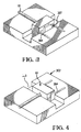
- the apparatus in final mounted form is shown in Figures 3 and 4 in perspective view.
- the basic essence of the present invention is that the surface emitting/receiving device 102 can be passively aligned to the fiber to submicron precision using the inside edges of the passive alignment member.
- the alignment of the device 102 is effected by the alignment pedestals 103 and 104.
- the device 102 is etched by RIE to have notches to receive the pedestals. In this way the device is precisely positioned with respect to the groove 108 of the PAM 101. Thereafter, the fiber 110 is seated in the groove 108 and the device 102 is aligned passively to the fiber 110.
- the device is then bonded to the PAM by solder reflow, and the vertical standoffs 106 are used optionally in cases where solder on the device would impede its emission/reception of light.
- the geometry of the PAM having the fiber inserted therein and the device 102 missing is as shown in Figure 6.
- the optical fiber 110 is shown mounted in a v-groove (not shown) that is etched by standard technique in the monocrystalline material that forms the substrate 302.
- the substrate is made 100 Si and is etched by wet etching techniques as is discussed in the reference to North, et al. discussed supra.
- the PAM 101 is mounted in a cavity 303 in the substrate. This cavity is formed by diamond saw cutting in the substrate in a perpendicular fashion to the direction of the v-shaped groove that holds the fiber 110.
- the electrical connections for making contact between the device 102 and external electronics is through the metalization 304 via metalization 107.
- the fiber 110 is readily aligned in the PAM.
- the fiber is bonded in the v-groove on the substrate.
- the fiber is thus placed in a well determined relationship with the groove 303, and thereafter the PAM is mounted in a well determined relationship in the groove, seating the fiber in its groove 108.
- the device is thereby passively aligned to the fiber.
- the fiber 110 is bonded to the v-groove as is shown in Figures 3,4 and 7.
- the bonding can be effected by soldering or other techniques such as electrostatic bonding techniques, or by solder techniques.
- the silicon substrate has a saw cut groove in the surface as shown at 303.
- the PAM having the device 102 mounted thereon are placed in the groove 303 and the fiber 110 then fits through the v-groove 108 effected as described above. This is shown clearly in Figure 6.
- the fiber is thereby passively aligned to the device 102.
- the PAM 101 may then be readily bonded to the groove 303 by presolder in the groove.
- Solder may also be placed on the contact areas 107 and 304 to enable electrical connection following reflow between the PAM and the silicon waferboard via the groove 303.
- the steps of manufacturing the device is discussed presently.
- Figure 5 we see the etched diamond shaped holes in quantity on a selected section of a wafer.
- the individual PAM's are then diced from the wafer.
- the wafer is preferably a monocrystalline Si wafer having a 110 plane on its top surface. This planar direction is chosen for purely illustrative purposes and it is understood that other planar orientations at variance with that chosen are within the purview of the skilled artisan and intended to be encompassed in the instant invention.
- the diamond shaped holes are etched through the wafer by wet etching as described in the North, et al. reference.
- the side and forward pedestals, 103 and 104 respectively, as well as the standoffs 106 are formed by reactive ion etching (RIE). Details of RIE techniques can be found in Optoelectronic Integration: Physics, Technology and Applications, Chapter 4, p. 113-119, Kluwer Academic Publishers, 1994, the disclosure of which is specifically incorporated herein by reference.
- RIE reactive ion etching
- the features made by RIE are effected first, then a mask such as SiN x which acts as a mask as well as a protective layer for the features etched by RIE.
- a photoresist is applied thereto the surface and the holes 501 are formed by revealing the preferred crystalline planes through the wet etching technique.
- the metallization patterns 107 are placed on the wafer by vacuum evaporation, sputtering or plating of conductive metals, preferably gold.
- the device 102 is mounted and passively aligned to the alignment features 103 and 104 and thereafter diebonded using a passive alignment diebonder. Thereafter the individual PAM's having the devices 102 mounted thereon are diced from the wafer by the use of a diamond saw.
- the vertical standoffs 106 have particular application in the alignment when a VCSEL is the preferred device 102.
- the fiber is fixed in position on the substrate 302 as described above, and the VCSEL is fixed in the x and y directions (assuming an orthogonal coordinate system) by the use of the side and forward pedestals.
- the height of the VCSEL in the z direction is carefully placed by the standoffs 106, as the VCSEL is bonded to the PAM with its epitaxial layer facing the fiber 110 (epi-side down), and as described above, the standoffs further have the inherent benefit to prevent solder from interfering with device emission/reception of light.
- FIG. 8-11 Figures 8 and 9 are a perspective and top view of an array link.
- a PAM 801 is disposed in groove 802 saw cut into the silicon substrate having preferably a 100 crystalline on its top surface wherein v-grooves are etched for receipt of fibers 805.
- the fibers are thereby aligned to an array of surface emitting/detecting devices 804.
- the processes and techniques for effecting the forward and side alignment pedestals and standoffs as well as the etching of the PAM are identical to that described for a single fiber/PAM/device as described above.
- the PAM 801 is shown on endview in Figure 10, having forward and side alignment pedestals 901 and 902, respectively, as well as optional standoffs 904.
- the metallization 905 is effected as described above.
- the PAM is fabricated on a wafer of (110) crystalline Si as is shown in Figure 11, and the technique for the fabrication of the PAM, the mounting of the devices 804 and the separating of the individual array PAM are effected in an identical procedure as described above for a single PAM.
- Figure 12 and 13 show the multiple fiber/multiple device configuration with the device 122 and fibers 123 mounted on the PAM 121 by forming an integral unit by techniques described for the single device/single fiber PAM as shown in Figures 1 and 2.
Landscapes
- Physics & Mathematics (AREA)
- General Physics & Mathematics (AREA)
- Optics & Photonics (AREA)
- Optical Couplings Of Light Guides (AREA)
Claims (8)
- Vorrichtung zur Ausrichtung eines optoelektronischen Bauteils (102) auf eine optische Faser (110), die aufweist: einen Träger mit einer Nut, in der die Faser angeordnet wird; und ein passives Ausrichtungselement (101), auf dem das optoelektronische Bauteil (102) montiert ist, dadurch gekennzeichnet, daß:das passive Ausrichtungselement (101) eine darin angeordnete Nut (108) für das Aufnehmen der optischen Faser (110) aufweist, und die Nut (108), die im Element (101) angeordnet ist, in der Ausrichtung orthogonal zum optoelektronischen Bauteil (102) verläuft.
- Vorrichtung nach Anspruch 1, außerdem dadurch gekennzeichnet, daß:das passive Ausrichtungselement (101) integrierte Ausrichtungselemente (103, 104, 106) aufweist, die auf der Oberfläche angeordnet sind.
- Vorrichtung nach Anspruch 2, außerdem dadurch gekennzeichnet, daß:die integrierten Ausrichtungselemente Sockel (103, 104) und Abstandselemente (106) sind.
- Vorrichtung nach Anspruch 2, außerdem dadurch gekennzeichnet, daß:die Ausrichtungselemente nach vorwärts gerichtete und seitliche Ausrichtungssockel (103, 104) sind.
- Vorrichtung nach Anspruch 2, außerdem dadurch gekennzeichnet, daß:die Ausrichtungselemente vertikale Abstandselemente (106) sind.
- Vorrichtung nach einem der vorhergehenden Ansprüche, außerdem dadurch gekennzeichnet, daß:ein passives Ausrichtungselement in einem Hohlraum im Träger montiert ist, wobei der Hohlraum orthogonal zur Nut im Träger ausrichtet ist.
- Vorrichtung nach einem der vorhergehenden Ansprüche, außerdem dadurch gekennzeichnet, daß:das passive Ausrichtungselement (101) ein einkristallines Material ist.
- Vorrichtung nach Anspruch 1, außerdem dadurch gekennzeichnet, daß:die Nut (108) im passiven Ausrichtungselement Seitenwände in gut definierten Kristallebenen aufweist.
Applications Claiming Priority (3)
| Application Number | Priority Date | Filing Date | Title |
|---|---|---|---|
| US77795P | 1995-06-30 | 1995-06-30 | |
| US777P | 1995-06-30 | ||
| PCT/US1996/010996 WO1997002501A1 (en) | 1995-06-30 | 1996-06-27 | Passive alignment frame using monocrystalline material |
Publications (2)
| Publication Number | Publication Date |
|---|---|
| EP1018050A1 EP1018050A1 (de) | 2000-07-12 |
| EP1018050B1 true EP1018050B1 (de) | 2001-12-12 |
Family
ID=21692989
Family Applications (1)
| Application Number | Title | Priority Date | Filing Date |
|---|---|---|---|
| EP96923492A Expired - Lifetime EP1018050B1 (de) | 1995-06-30 | 1996-06-27 | Vorrichtung zur ausrichtung eines optoelektronischen bauteils |
Country Status (5)
| Country | Link |
|---|---|
| US (1) | US5905831A (de) |
| EP (1) | EP1018050B1 (de) |
| JP (1) | JP3730664B2 (de) |
| DE (1) | DE69618035T2 (de) |
| WO (1) | WO1997002501A1 (de) |
Families Citing this family (38)
| Publication number | Priority date | Publication date | Assignee | Title |
|---|---|---|---|---|
| WO1998045740A1 (de) * | 1997-04-08 | 1998-10-15 | Paul Scherrer Institut | Vorrichtung zum verbinden von optischen elementen und verfahren zur herstellung derselben |
| US6178188B1 (en) * | 1997-12-11 | 2001-01-23 | Photera Technologies, Inc | Laser assembly platform with silicon base |
| US5913002A (en) * | 1997-12-31 | 1999-06-15 | The Whitaker Corporation | Optical coupling device for passive alignment of optoelectronic devices and fibers |
| US6085007A (en) * | 1998-02-27 | 2000-07-04 | Jiang; Ching-Long | Passive alignment member for vertical surface emitting/detecting device |
| US6151430A (en) | 1998-07-08 | 2000-11-21 | Gore Enterprise Holdings, Inc. | Photonic device having an integal guide and method of manufacturing |
| US6377732B1 (en) | 1999-01-22 | 2002-04-23 | The Whitaker Corporation | Planar waveguide devices and fiber attachment |
| WO2001059487A2 (en) * | 2000-02-11 | 2001-08-16 | Bandwidth9, Inc. | Waveguide assembly |
| US6726372B1 (en) | 2000-04-06 | 2004-04-27 | Shipley±Company, L.L.C. | 2-Dimensional optical fiber array made from etched sticks having notches |
| DE50016039D1 (de) * | 2000-10-09 | 2011-01-05 | Siemens Ag | Positionsfixierung in leiterplatten |
| US6393175B1 (en) | 2000-11-15 | 2002-05-21 | Optical Switch Corporation | Integrated fiber array optical switch and method of operation |
| US6516111B1 (en) | 2000-11-15 | 2003-02-04 | Optical Switch Corporation | Cascaded integrated fiber array optical switch and method of operation |
| US6516107B1 (en) | 2000-11-15 | 2003-02-04 | Optical Switch Corporation | 2×2 integrated fiber array optical switch and method of operation |
| US6393174B1 (en) | 2000-11-15 | 2002-05-21 | Optical Switch Corporation | Integrated fiber array optical switch using double-pass propagation and method of operation |
| US6917056B2 (en) | 2001-01-31 | 2005-07-12 | Shipley Company, L.L.C. | Optoelectronic submount having an on-edge optoelectronic device |
| US6788847B2 (en) * | 2001-04-05 | 2004-09-07 | Luxtera, Inc. | Photonic input/output port |
| DE10134637A1 (de) * | 2001-07-17 | 2003-03-27 | Harting Elektrooptische Bauteile Gmbh & Co Kg | Substrat für eine opto-elektronische Baugruppe |
| US7813634B2 (en) | 2005-02-28 | 2010-10-12 | Tessera MEMS Technologies, Inc. | Autofocus camera |
| US6661955B1 (en) | 2002-02-04 | 2003-12-09 | Siwave, Inc. | Kinematic and non-kinematic passive alignment assemblies and methods of making the same |
| US6674585B1 (en) | 2002-02-04 | 2004-01-06 | Siwave, Inc. | Flexure assemblies and methods of making the same |
| US6850675B1 (en) | 2002-02-04 | 2005-02-01 | Siwave, Inc. | Base, payload and connecting structure and methods of making the same |
| TW523111U (en) * | 2002-02-26 | 2003-03-01 | Ind Tech Res Inst | Passive alignment packaging structure of photoelectric device and fiber connector |
| US6909827B2 (en) * | 2002-05-01 | 2005-06-21 | Adc Telecommunications, Inc. | Compact optical module with adjustable joint for decoupled alignment |
| US20050025430A1 (en) * | 2002-07-23 | 2005-02-03 | Bhagavatula Venkata A. | Apparatus and methods for passive alignment of optical elements |
| ATE492828T1 (de) * | 2004-06-25 | 2011-01-15 | Andrea Pizzarulli | Verfahren zum zusammenbau optoelektonischer baugruppen und optoelektronische baugruppe |
| CN100373132C (zh) * | 2004-11-25 | 2008-03-05 | 电子科技大学 | 一种探测器-光纤耦合的全方位自对准方法 |
| DE102005002874B3 (de) * | 2005-01-21 | 2006-09-14 | Forschungszentrum Karlsruhe Gmbh | Optoelektronisches Bauelement mit integrierter Wellenleiter-Ankopplung für passive Justage |
| JP2009122451A (ja) * | 2007-11-15 | 2009-06-04 | Hitachi Chem Co Ltd | 光学接続構造 |
| JP2011033876A (ja) * | 2009-08-03 | 2011-02-17 | Nitto Denko Corp | 光センサモジュールの製造方法およびそれによって得られた光センサモジュール |
| JP2011186036A (ja) * | 2010-03-05 | 2011-09-22 | Nitto Denko Corp | 光センサモジュールの製法およびそれによって得られた光センサモジュール |
| JP5308408B2 (ja) | 2010-07-27 | 2013-10-09 | 日東電工株式会社 | 光センサモジュール |
| JP5325184B2 (ja) | 2010-08-31 | 2013-10-23 | 日東電工株式会社 | 光センサモジュール |
| JP2012068391A (ja) * | 2010-09-22 | 2012-04-05 | Murata Mfg Co Ltd | プラグ及び光伝送モジュール |
| JP5693986B2 (ja) | 2011-02-03 | 2015-04-01 | 日東電工株式会社 | 光センサモジュール |
| US9364925B2 (en) * | 2012-04-30 | 2016-06-14 | Globalfoundries Inc. | Assembly of electronic and optical devices |
| US8798410B2 (en) | 2012-06-12 | 2014-08-05 | Laxense Inc. | Optical system with integrated photodetector using a self-aligned double U-groove structure |
| US9134490B2 (en) | 2012-12-06 | 2015-09-15 | Laxense Inc. | Passive alignment multichannel parallel optical system |
| US9335494B2 (en) | 2014-05-15 | 2016-05-10 | Tyco Electronics Corporation | Optoelectronics structures |
| US9709758B2 (en) | 2014-12-16 | 2017-07-18 | Te Connectivity Nederland B.V. | Optical assembly with passive alignment |
Citations (2)
| Publication number | Priority date | Publication date | Assignee | Title |
|---|---|---|---|---|
| US4079404A (en) * | 1976-12-30 | 1978-03-14 | International Business Machines Corporation | Self-aligning support structure for optical components |
| EP0466134A2 (de) * | 1990-07-11 | 1992-01-15 | Gte Laboratories Incorporated | Methode und Vorrichtung zum passiven Ausrichten von Diodenlasern und optischen Fasern |
Family Cites Families (20)
| Publication number | Priority date | Publication date | Assignee | Title |
|---|---|---|---|---|
| US4210923A (en) * | 1979-01-02 | 1980-07-01 | Bell Telephone Laboratories, Incorporated | Edge illuminated photodetector with optical fiber alignment |
| JPS55157277A (en) * | 1979-05-25 | 1980-12-06 | Fujitsu Ltd | Optical semiconductor device |
| JPS59185306A (ja) * | 1983-04-07 | 1984-10-20 | Agency Of Ind Science & Technol | 光集積回路の実装法 |
| ES2011773B3 (es) * | 1985-10-16 | 1990-02-16 | British Telecomm | Selector de longitudes de onda |
| JPS63239890A (ja) * | 1987-03-27 | 1988-10-05 | Hitachi Ltd | 光素子モジユ−ルおよびその製造方法 |
| GB2208943B (en) * | 1987-08-19 | 1991-07-31 | Plessey Co Plc | Alignment of fibre arrays |
| US4904036A (en) * | 1988-03-03 | 1990-02-27 | American Telephone And Telegraph Company, At&T Bell Laboratories | Subassemblies for optoelectronic hybrid integrated circuits |
| JPH024204A (ja) * | 1988-06-21 | 1990-01-09 | Hitachi Ltd | 光・電子回路の実装方法 |
| US5073003A (en) * | 1988-12-23 | 1991-12-17 | At&T Bell Laboratories | Optoelectronic device package method and apparatus |
| US5182782A (en) * | 1990-07-11 | 1993-01-26 | Gte Laboratories Incorporated | Waferboard structure and method of fabricating |
| US5179609A (en) * | 1991-08-30 | 1993-01-12 | At&T Bell Laboratories | Optical assembly including fiber attachment |
| CH685522A5 (fr) * | 1991-09-10 | 1995-07-31 | Suisse Electronique Microtech | Procédé pour positionner un premier substrat sur un second substrat et dispositif micromécanique de positionnement obtenu. |
| JPH05249340A (ja) * | 1992-03-06 | 1993-09-28 | Sumitomo Electric Ind Ltd | 光部品の結合装置 |
| JP3129538B2 (ja) * | 1992-10-07 | 2001-01-31 | 日本碍子株式会社 | 光ファイバアレイ及びその製造方法 |
| US5412748A (en) * | 1992-12-04 | 1995-05-02 | Kabushiki Kaisha Toshiba | Optical semiconductor module |
| DE4301236C1 (de) * | 1993-01-19 | 1994-03-17 | Ant Nachrichtentech | Vorrichtung zur optischen Kopplung eines Lichtwellenleiters mit einem optoelektrischen Wandler |
| US5555333A (en) * | 1993-07-12 | 1996-09-10 | Ricoh Company, Ltd. | Optical module and a fabrication process thereof |
| JP3302458B2 (ja) * | 1993-08-31 | 2002-07-15 | 富士通株式会社 | 集積化光装置及び製造方法 |
| US5420953A (en) * | 1994-02-17 | 1995-05-30 | The Whitaker Corporation | Optoelectronic integration of holograms using (110) oriented silicon on (100) oriented silicon waferboard |
| US5533158A (en) * | 1994-09-12 | 1996-07-02 | The Whitaker Corporation | Electrostatic bonding of optical fibers to substrates |
-
1996
- 1996-06-27 EP EP96923492A patent/EP1018050B1/de not_active Expired - Lifetime
- 1996-06-27 WO PCT/US1996/010996 patent/WO1997002501A1/en not_active Ceased
- 1996-06-27 JP JP50521597A patent/JP3730664B2/ja not_active Expired - Fee Related
- 1996-06-27 DE DE69618035T patent/DE69618035T2/de not_active Expired - Lifetime
- 1996-06-28 US US08/674,770 patent/US5905831A/en not_active Expired - Fee Related
Patent Citations (2)
| Publication number | Priority date | Publication date | Assignee | Title |
|---|---|---|---|---|
| US4079404A (en) * | 1976-12-30 | 1978-03-14 | International Business Machines Corporation | Self-aligning support structure for optical components |
| EP0466134A2 (de) * | 1990-07-11 | 1992-01-15 | Gte Laboratories Incorporated | Methode und Vorrichtung zum passiven Ausrichten von Diodenlasern und optischen Fasern |
Also Published As
| Publication number | Publication date |
|---|---|
| DE69618035T2 (de) | 2002-07-11 |
| JP3730664B2 (ja) | 2006-01-05 |
| WO1997002501A1 (en) | 1997-01-23 |
| EP1018050A1 (de) | 2000-07-12 |
| US5905831A (en) | 1999-05-18 |
| DE69618035D1 (de) | 2002-01-24 |
| JPH11509007A (ja) | 1999-08-03 |
Similar Documents
| Publication | Publication Date | Title |
|---|---|---|
| US5905831A (en) | Passive alignment frame using monocrystalline material | |
| US6741778B1 (en) | Optical device with chip level precision alignment | |
| US5913002A (en) | Optical coupling device for passive alignment of optoelectronic devices and fibers | |
| EP0226296B1 (de) | Optische Komponente mit Wellenleiter | |
| US5071213A (en) | Optical coupler and method of making optical coupler | |
| CA2046716C (en) | Method and device for passive alignment of diode lasers and optical fibers | |
| JP3341250B2 (ja) | 光電子モジュール | |
| EP0826995B1 (de) | Optoelektronisches Modul dessen Bauelemente auf einem einzigen Trägerelement montiert sind | |
| CN103718076B (zh) | 透明光学插入件 | |
| JP2001515608A (ja) | 光電素子の直接結合用レセプタクル | |
| EP0950204A1 (de) | Flexible optische verbindungseinheit | |
| US6085007A (en) | Passive alignment member for vertical surface emitting/detecting device | |
| JP2000106468A (ja) | レ―ザ―ダイオ―ドチップの製造方法、光送/受信モジュ―ル及びこれらの位置整列方法 | |
| JP2014503858A (ja) | 光インタポーザ | |
| EP0893720B1 (de) | Ein Mikro-Photonikmodul mit einer Trennwand | |
| TW201307926A (zh) | 具共同傾斜表面之光學插入元件 | |
| US6249627B1 (en) | Arrangement for self-aligning optical fibers to an array of surface emitting lasers | |
| WO2008007056A2 (en) | Mounting surface-emitting devices | |
| US9651749B1 (en) | Interposer with opaque substrate | |
| WO2000031771A1 (en) | Optoelectronic module and method of making same | |
| US20030068142A1 (en) | Optical subassembly for fiber arrays with a 90 degree conductor turn | |
| JP3801922B2 (ja) | 光モジュール | |
| CA1276781C (en) | Positioning optical components and waveguides | |
| JPH06250049A (ja) | 光伝送モジュール及びその作製方法 |
Legal Events
| Date | Code | Title | Description |
|---|---|---|---|
| PUAI | Public reference made under article 153(3) epc to a published international application that has entered the european phase |
Free format text: ORIGINAL CODE: 0009012 |
|
| 17P | Request for examination filed |
Effective date: 19980130 |
|
| AK | Designated contracting states |
Kind code of ref document: A1 Designated state(s): DE FR GB |
|
| RIN1 | Information on inventor provided before grant (corrected) |
Inventor name: HAN, HONGTAO Inventor name: BOWEN, TERRY, PATRICK Inventor name: BOUDREAU, ROBERT, ADDISON |
|
| RTI1 | Title (correction) |
Free format text: APPARATUS FOR ALIGNING AN OPTOELECTRONIC DEVICE |
|
| GRAG | Despatch of communication of intention to grant |
Free format text: ORIGINAL CODE: EPIDOS AGRA |
|
| 17Q | First examination report despatched |
Effective date: 20010212 |
|
| GRAG | Despatch of communication of intention to grant |
Free format text: ORIGINAL CODE: EPIDOS AGRA |
|
| GRAH | Despatch of communication of intention to grant a patent |
Free format text: ORIGINAL CODE: EPIDOS IGRA |
|
| GRAH | Despatch of communication of intention to grant a patent |
Free format text: ORIGINAL CODE: EPIDOS IGRA |
|
| GRAA | (expected) grant |
Free format text: ORIGINAL CODE: 0009210 |
|
| AK | Designated contracting states |
Kind code of ref document: B1 Designated state(s): DE FR GB |
|
| REG | Reference to a national code |
Ref country code: GB Ref legal event code: IF02 |
|
| REF | Corresponds to: |
Ref document number: 69618035 Country of ref document: DE Date of ref document: 20020124 |
|
| PLBE | No opposition filed within time limit |
Free format text: ORIGINAL CODE: 0009261 |
|
| STAA | Information on the status of an ep patent application or granted ep patent |
Free format text: STATUS: NO OPPOSITION FILED WITHIN TIME LIMIT |
|
| 26N | No opposition filed | ||
| PGFP | Annual fee paid to national office [announced via postgrant information from national office to epo] |
Ref country code: FR Payment date: 20100630 Year of fee payment: 15 |
|
| PGFP | Annual fee paid to national office [announced via postgrant information from national office to epo] |
Ref country code: GB Payment date: 20100625 Year of fee payment: 15 Ref country code: DE Payment date: 20100629 Year of fee payment: 15 |
|
| GBPC | Gb: european patent ceased through non-payment of renewal fee |
Effective date: 20110627 |
|
| REG | Reference to a national code |
Ref country code: FR Ref legal event code: ST Effective date: 20120229 |
|
| REG | Reference to a national code |
Ref country code: DE Ref legal event code: R119 Ref document number: 69618035 Country of ref document: DE Effective date: 20120103 |
|
| PG25 | Lapsed in a contracting state [announced via postgrant information from national office to epo] |
Ref country code: DE Free format text: LAPSE BECAUSE OF NON-PAYMENT OF DUE FEES Effective date: 20120103 Ref country code: FR Free format text: LAPSE BECAUSE OF NON-PAYMENT OF DUE FEES Effective date: 20110630 |
|
| PG25 | Lapsed in a contracting state [announced via postgrant information from national office to epo] |
Ref country code: GB Free format text: LAPSE BECAUSE OF NON-PAYMENT OF DUE FEES Effective date: 20110627 |