EP1061436A2 - Pipeline d'addition/soustraction à virgule flottante multifunction - Google Patents
Pipeline d'addition/soustraction à virgule flottante multifunction Download PDFInfo
- Publication number
- EP1061436A2 EP1061436A2 EP00203249A EP00203249A EP1061436A2 EP 1061436 A2 EP1061436 A2 EP 1061436A2 EP 00203249 A EP00203249 A EP 00203249A EP 00203249 A EP00203249 A EP 00203249A EP 1061436 A2 EP1061436 A2 EP 1061436A2
- Authority
- EP
- European Patent Office
- Prior art keywords
- unit
- value
- floating point
- output
- close
- Prior art date
- Legal status (The legal status is an assumption and is not a legal conclusion. Google has not performed a legal analysis and makes no representation as to the accuracy of the status listed.)
- Granted
Links
Images




























Classifications
-
- H—ELECTRICITY
- H03—ELECTRONIC CIRCUITRY
- H03M—CODING; DECODING; CODE CONVERSION IN GENERAL
- H03M7/00—Conversion of a code where information is represented by a given sequence or number of digits to a code where the same, similar or subset of information is represented by a different sequence or number of digits
- H03M7/14—Conversion to or from non-weighted codes
- H03M7/24—Conversion to or from floating-point codes
-
- G—PHYSICS
- G06—COMPUTING OR CALCULATING; COUNTING
- G06F—ELECTRIC DIGITAL DATA PROCESSING
- G06F7/00—Methods or arrangements for processing data by operating upon the order or content of the data handled
- G06F7/38—Methods or arrangements for performing computations using exclusively denominational number representation, e.g. using binary, ternary, decimal representation
- G06F7/48—Methods or arrangements for performing computations using exclusively denominational number representation, e.g. using binary, ternary, decimal representation using non-contact-making devices, e.g. tube, solid state device; using unspecified devices
- G06F7/483—Computations with numbers represented by a non-linear combination of denominational numbers, e.g. rational numbers, logarithmic number system or floating-point numbers
-
- G—PHYSICS
- G06—COMPUTING OR CALCULATING; COUNTING
- G06F—ELECTRIC DIGITAL DATA PROCESSING
- G06F9/00—Arrangements for program control, e.g. control units
- G06F9/06—Arrangements for program control, e.g. control units using stored programs, i.e. using an internal store of processing equipment to receive or retain programs
- G06F9/30—Arrangements for executing machine instructions, e.g. instruction decode
- G06F9/30003—Arrangements for executing specific machine instructions
- G06F9/30007—Arrangements for executing specific machine instructions to perform operations on data operands
- G06F9/3001—Arithmetic instructions
- G06F9/30014—Arithmetic instructions with variable precision
-
- G—PHYSICS
- G06—COMPUTING OR CALCULATING; COUNTING
- G06F—ELECTRIC DIGITAL DATA PROCESSING
- G06F9/00—Arrangements for program control, e.g. control units
- G06F9/06—Arrangements for program control, e.g. control units using stored programs, i.e. using an internal store of processing equipment to receive or retain programs
- G06F9/30—Arrangements for executing machine instructions, e.g. instruction decode
- G06F9/30003—Arrangements for executing specific machine instructions
- G06F9/30007—Arrangements for executing specific machine instructions to perform operations on data operands
- G06F9/30021—Compare instructions, e.g. Greater-Than, Equal-To, MINMAX
-
- G—PHYSICS
- G06—COMPUTING OR CALCULATING; COUNTING
- G06F—ELECTRIC DIGITAL DATA PROCESSING
- G06F9/00—Arrangements for program control, e.g. control units
- G06F9/06—Arrangements for program control, e.g. control units using stored programs, i.e. using an internal store of processing equipment to receive or retain programs
- G06F9/30—Arrangements for executing machine instructions, e.g. instruction decode
- G06F9/30003—Arrangements for executing specific machine instructions
- G06F9/30007—Arrangements for executing specific machine instructions to perform operations on data operands
- G06F9/30036—Instructions to perform operations on packed data, e.g. vector, tile or matrix operations
-
- G—PHYSICS
- G06—COMPUTING OR CALCULATING; COUNTING
- G06F—ELECTRIC DIGITAL DATA PROCESSING
- G06F9/00—Arrangements for program control, e.g. control units
- G06F9/06—Arrangements for program control, e.g. control units using stored programs, i.e. using an internal store of processing equipment to receive or retain programs
- G06F9/30—Arrangements for executing machine instructions, e.g. instruction decode
- G06F9/30003—Arrangements for executing specific machine instructions
- G06F9/30007—Arrangements for executing specific machine instructions to perform operations on data operands
- G06F9/30036—Instructions to perform operations on packed data, e.g. vector, tile or matrix operations
- G06F9/30038—Instructions to perform operations on packed data, e.g. vector, tile or matrix operations using a mask
-
- G—PHYSICS
- G06—COMPUTING OR CALCULATING; COUNTING
- G06F—ELECTRIC DIGITAL DATA PROCESSING
- G06F9/00—Arrangements for program control, e.g. control units
- G06F9/06—Arrangements for program control, e.g. control units using stored programs, i.e. using an internal store of processing equipment to receive or retain programs
- G06F9/30—Arrangements for executing machine instructions, e.g. instruction decode
- G06F9/3017—Runtime instruction translation, e.g. macros
-
- G—PHYSICS
- G06—COMPUTING OR CALCULATING; COUNTING
- G06F—ELECTRIC DIGITAL DATA PROCESSING
- G06F9/00—Arrangements for program control, e.g. control units
- G06F9/06—Arrangements for program control, e.g. control units using stored programs, i.e. using an internal store of processing equipment to receive or retain programs
- G06F9/30—Arrangements for executing machine instructions, e.g. instruction decode
- G06F9/38—Concurrent instruction execution, e.g. pipeline or look ahead
- G06F9/3802—Instruction prefetching
- G06F9/3804—Instruction prefetching for branches, e.g. hedging, branch folding
-
- G—PHYSICS
- G06—COMPUTING OR CALCULATING; COUNTING
- G06F—ELECTRIC DIGITAL DATA PROCESSING
- G06F9/00—Arrangements for program control, e.g. control units
- G06F9/06—Arrangements for program control, e.g. control units using stored programs, i.e. using an internal store of processing equipment to receive or retain programs
- G06F9/30—Arrangements for executing machine instructions, e.g. instruction decode
- G06F9/38—Concurrent instruction execution, e.g. pipeline or look ahead
- G06F9/3885—Concurrent instruction execution, e.g. pipeline or look ahead using a plurality of independent parallel functional units
Definitions
- This invention relates to floating point arithmetic within microprocessors, and more particularly to an add/subtract pipeline and multifunction bipartite look-up table within a floating point arithmetic unit.
- Numbers may be represented within computer systems in a variety of ways.
- a 32-bit register may store numbers ranging from 0 to 2 32 -1. (The same register may also signed numbers by giving up one order of magnitude in range). This format is limiting, however, since it is incapable of representing numbers which are not integers (the binary point in integer format may be thought of as being to the right of the least significant bit in the register).
- a fixed point representation may be used.
- the binary point is considered to be somewhere other than to the right of the least significant bit.
- a 32-bit register may be used to store values from 0 (inclusive) to 2 (exclusive) by processing register values as though the binary point is located to the right of the most significant register bit.
- Such a representation allows (in this example) 31 registers bit to represent fractional values.
- one bit may be used as a sign bit so that a register can store values between -2 and +2.
- floating point numeric representations include three parts: a sign bit, an unsigned fractional number, and an exponent value.
- IEEE standard 754 single precision
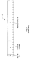
- FIG. 1 floating point format 2 is shown.
- Format 2 includes a sign bit 4 (denoted as S), an exponent portion 6 (E), and a mantissa portion 8 (F).
- Sign bit S represents the sign of the entire number
- mantissa portion F is a 23-bit number with an implied leading 1 bit (values with a leading one bit are said to be "normalized”). In other embodiments, the leading one bit may be explicit.
- Exponent portion E is an 8-bit value which represents the true exponent of the number V offset by a predetermined bias. A bias is used so that both positive and negative true exponents of floating point numbers may be easily compared.
- the number 127 is used as the bias in IEEE standard 754. Format 2 may thus accommodate numbers having exponents from -127 to +128. Floating point format 2 advantageously allows 24 bits of representation within each of these orders of magnitude.
- Floating point addition is an extremely common operation in numerically-intensive applications. (Floating point subtraction is accomplished by inverting one of the inputs and performing addition). Although floating point addition is related to fixed point addition, two differences cause complications. First, an exponent value of the result must be determined from the input operands. Secondly, rounding must be performed. The IEEE standard specifies that the result of an operation should be the same as if the result were computed exactly, and then rounded (to a predetermined number of digits) using the current rounding mode. IEEE standard 754 specifies four rounding modes: round to nearest, round to zero, round to + ⁇ , and round to - ⁇ . The default mode, round to nearest, chooses the even number in the event of a tie.
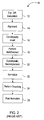
- FIG. 2 a prior art floating point addition pipeline 10 is depicted. All steps in pipeline 10 are not performed for all possible additions. (That is, some steps are optional for various cases of inputs). The stages of pipeline 10 are described below with reference to input values A and B.
- Input value A has a sign bit A S , an exponent value A E , and a mantissa value A F .
- Input value B similarly, has a sign bit B S , exponent value B E , and mantissa value B F .
- Pipeline 10 first includes a stage 12, in which an exponent difference E diff is calculated between A E and B E .
- E diff is calculated to be negative
- operands A and B are swapped such that A is now the larger operand.
- the operands are swapped such that E diff is always positive.
- stage 16 the shifted version of operand B is inverted, if needed, to perform subtraction.
- the signs of the input operands and the desired operation are examined in order to determine whether effective addition or effective subtraction is occurring.
- the operation A minus B, where B is negative, is equivalent to A plus B (ignoring the sign bit of B). Therefore, effective addition is performed.
- the inversion in stage 16 may be either of the one's complement or two's complement variety.
- stage 18 the addition of operand A and operand B is performed. As described above, operand B may be shifted and may be inverted as needed. Next, in stage 20, the result of stage 18 may be recomplemented, meaning that the value is returned to sign-magnitude form (as opposed to one's or two's complement form).
- stage 22 the result of stage 20 is normalized. This includes left-shifting the result of stage 20 until the most significant bit is a 1.
- the bits which are shifted in are calculated according to the values of G, R, and S.
- stage 24 If the rounding performed in stage 24 produces an overflow, the result is post-normalized (right-shifted) in stage 26.
- floating point addition is quite complicated. This operation is quite time-consuming, also, if performed as shown in Fig. 2: stage 14 (alignment) requires a shift, stage 18 requires a full add, stage 20 (recomplementation) requires a full add, stage 22 requires a shift, and stage 24 (rounding) requires a full add. Consequently, performing floating point addition using pipeline 10 would cause add/subtract operations to have a similar latency to floating point multiplication. Because of the frequency of floating point addition, higher performance is typically desired. Accordingly, most actual floating point add pipeline include optimizations to pipeline 10.
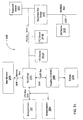
- FIG. 3 a prior art floating point pipeline 30 is depicted which is optimized with respect to pipeline 10.
- pipeline 30 includes two paths which operate concurrently, far path 31A and close path 31B.
- Far path 31A is configured to perform all effective additions.
- Far path 31A is additionally configured to perform effective subtractions for which E diff >1.
- Close path 31B conversely is configured to perform effective subtractions for which E diff ⁇ 1.
- the operation of pipeline 30 is described with respect to input values A and B.
- Pipeline 30 first includes stage 32, in which operands A and B are received. The operands are conveyed to both far path 31A and close path 31B. Results are then computed for both paths, with the final result selected in accordance with the actual exponent difference. The operation of far path 31A is described first.
- exponent difference E diff is computed for operands A and B.
- the operands are swapped if A E >B E . If E diff is computed to be 0 or 1, execution in far path 31 A is cancelled, since this case is handled by close path 31B as will be described below.
- stage 36 the input values are aligned by right shifting operand B as needed.
- stage 38 operand B is conditionally inverted in the case of effective subtraction (operand B is not inverted in the case of effective addition).
- stage 40 the actual addition is performed. Because of the restrictions placed on far path (E diff >1), the result of stage 40 is always positive. Thus, no recomplementation step is needed.
- the result of stage 40 is instead rounded and post-normalized in stages 42 and 44, respectively.
- the result of far path 31A is then conveyed to stage 58.
- exponent difference E diff is calculated in stage 46. If E diff is computed to less than equal to 1, execution continues in close path 31B with stage 48.
- operands A and B are swapped (as in one embodiment of far path 31A) so that A E ⁇ B E .
- operand B is inverted to set up the subtraction which is performed in stage 50.
- the smaller operand is also shifted by at most one bit. Since the possible shift amount is low, however, this operation may be accomplished with greatly reduced hardware.
- stage 50 The output of stage 50 is then recomplemented if needed in stage 52, and then normalized in stage 54. This result is rounded in stage 56, with the rounded result conveyed to stage 58. In stage 58, either the far path or close path result is selected according to the value of E diff .
- stage 52 (recomplementation) and stage 56 (rounding) are mutually exclusive.
- shifting giving rise to the possibility of rounding
- the result of stage 50 is always positive, eliminating the need for recomplementation in stage 52.
- pipeline 30 allows each path 31 to exclude unneeded hardware. For example, far path 31A does not require an additional adder for recomplementation as described above. Close path 31B eliminates the need for a full shift operation before stage 50, and also reduces the number of add operations required (due to the exclusivity of rounding and recomplementation described above).
- Pipeline 30 offers improved performance over pipeline 10. Because of the frequency of floating point add/subtract operations, however, a floating point addition pipeline is desired which exhibits improved performance over pipeline 30. Improved performance is particularly desired with respect to close path 31B.
- Floating-point instructions are used within microprocessors to perform high-precision mathematical operations for a variety of numerically-intensive applications. Floating-point arithmetic is particularly important within applications that perform the rendering of three-dimensional graphical images. Accordingly, as graphics processing techniques grow more sophisticated, a corresponding increase in floating-point performance is required.
- the graphics pipeline may be considered as having a front end and a back end.
- the front end receives a set of vertices and associated parameters which define a graphical object in model space coordinates.
- these vertices are assembled into graphical primitives (such as triangles) which are converted into screen space coordinates.
- graphical primitives such as triangles
- One distinguishing feature of these front-end operations is that they are primarily performed using floating-point numbers.
- the back end of the pipeline is typically integer-intensive and involves the rasterization (drawing on a display device) of geometric primitives produced by the front end of the pipeline.
- High-end graphics systems typically include graphics accelerators coupled to the microprocessor via the system bus. These graphics accelerators include dedicated hardware specifically designed for efficiently performing operations of the graphics pipeline. Most consumer-level graphics cards, however, only accelerate the rasterization stages of the graphics pipeline. In these systems, the microprocessor is responsible for performing the floating-point calculations in the initial stages of the graphics pipeline. The microprocessor then conveys the graphics primitives produced from these calculations to the graphics card for rasterizing. For such systems, it is clear that increased microprocessor floating-point performance may result in increased graphics processing capability.
- floating-point hardware is relatively large as compared to comparable fixed-point hardware, however, such an implementation may use a significant portion of the hardware real estate allocated to the floating-point unit.
- An alternate approach is to utilize an existing floating-point element (such as a multiplier) to implement division based on iterative techniques like the Goldschmidt or Newton-Raphson algorithms.
- Iterative algorithms for division require a starting approximation for the reciprocal of the divisor.
- a predetermined equation is then evaluated using this starting approximation.
- the result ofthis evaluation is then used for a subsequent evaluation of the predetermined equation. This process is repeated until a result of the desired accuracy is reached.
- the number of iterations needed to achieve the final result must be small.
- One means to decrease the number of iterations in the division operation is to increase the accuracy of the starting approximation. The more accurately the first approximation is determined, then, the more quickly the division may be performed.
- a look-up table is a read-only memory (ROM) which stores a predetermined output value for each of a number of regions within a given input range.
- ROM read-only memory
- the look-up table is located within the microprocessor's floating-point unit.
- An input range for a floating-point function is typically bounded by a single binade of floating point values (a "binade” refers to a range of numbers between consecutive powers of 2). Input ranges for other floating-point functions, however, may span more than one binade.
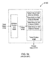
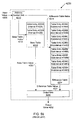
- Bipartite look-up tables In order to decrease table size while still maintaining accuracy, "bipartite" look-up tables are utilized. Bipartite look-up tables actually include two separate tables: a base value table and a difference value table.
- the base table includes function output values (or "nodes") for various regions of the input range.
- the values in the difference table are then used to calculate function output values located between nodes in the base table. This calculation may be performed by linear interpolation or various other techniques.
- table storage requirements may be dramatically reduced while maintaining a high level of accuracy. If the function changes slowly, for example, the number of bits required for difference table entries is much less than the number of bits in the base table entries. This allows the bipartite table to be implemented with fewer bits than a comparable naive table (one which does not employ interpolation).
- Prior art bipartite look-up tables provide output values having a minimal amount of maximum relative error over a given input interval. This use of relative error to measure the accuracy of the look-up table output values is questionable, however, because of a problem known as "wobbling precision". Wobbling precision refers to the fact that a difference in the least significant bit of an input value to the look-up table has twice the relative error at the end of a binade than it has at the start of the binade. A look-up table constructed in this manner is thus not as accurate as possible.
- multi-function look-up table which implements both the reciprocal and reciprocal square root functions with minimal overhead. It would further be desirable for the multi-function look-up table to be a bipartite look-up table.
- an execution unit which is usable to perform effective addition or subtraction upon a given pair of floating point input values.
- the execution unit includes an add/subtract pipeline having a far data path and a close data path each coupled to receive the given pair of floating point input values.
- the far data path is configured to perform effective addition as well as effective subtraction upon operands having an absolute exponent difference greater than one.
- the close data path is configured to perform effective subtraction upon operands having an absolute exponent difference less than or equal to one.
- the add/subtract pipeline further includes a result multiplexer unit coupled to receive a result from both the far data path and the close data path. A final output of the result multiplexer unit is selected from the far path result and the close path result according to the actual calculated absolute exponent difference value.
- the far data path includes a pair of right shift units coupled to receive mantissa portions of each of the given pair of floating point input values.
- the right shift units each receive a shift amount from a corresponding exponent difference unit.
- the first right shift unit conveys a shift amount equal to the second exponent value minus the first exponent value
- the second right shift unit conveys a shift amount equal to the first exponent value minus the second exponent value.
- the outputs of the right shift units are then conveyed to a multiplexer-inverter unit, which also receives unshifted versions of the mantissa portions of each of the given pair of floating point input values.
- the multiplexer-inverter unit is configured to select one of the unshifted mantissa portions and one of the shifted mantissa portions to be conveyed as inputs to an adder unit.
- the adder inputs conveyed by the multiplexer-inverter unit are aligned in order to facilitate the addition operation.
- the multiplexer-inverter unit is further configured to invert the second adder input if the effective operation to be performed is subtraction.
- the adder unit is configured to add the first and second adder inputs, thereby generating first and second adder outputs.
- the first adder output is equal to the sum of the two inputs, while the second adder output is equal to the first adder output plus one.
- One of the two adder outputs is selected according to a far path selection signal generated by a far path selection unit.
- the far path selection unit is configured to generate a plurality of preliminary far path selection signals. Each of these preliminary far path selection signals corresponds to a different possible normalization of the first adder output. For example, one of the preliminary far path selection signals corresponds to a prediction that the first adder output is properly normalized.
- Another preliminary far path selection signal corresponds to a prediction that the first adder output is not normalized, while still another select signal indicates that said first adder output has an overflow bit set.
- One of these preliminary far path selection signals is selected to be conveyed as the final far path selection signal based on which of these predictions actually occurs.
- the far data path further includes a multiplexer-shift unit configured to receive the first and second adder outputs as well as the final far path selection signal.
- the appropriate adder output is selected, and a one-bit left or right shift may also be performed to properly normalize the result.
- a guard bit previously shifted out of one of the mantissa values by a right shift unit may be shifted back into the final result.
- the selected value is conveyed as a mantissa portion of the far data path result value.
- the exponent portion of the far path result is calculated by a exponent adjustment unit.
- the exponent adjustment unit is configured to receive the original larger exponent value along with the amount of shifting required for proper normalization (which may be no shift, a one-bit left shift, or a one-bit right shift).
- the far data path is optimized to perform effective additions.
- the far data path is additionally optimized to perform effective subtractions on operands having an absolute exponent difference greater than one. This configuration allows the recomplementation step to be avoided, since all operations produce positive results. Furthermore, since adder outputs require at most a one-bit shift, only one full-size shifter is needed in the far data path. This results in improved floating point addition and subtraction performance for the far data path.
- the close data path is coupled to receive mantissa portions of the given pair of floating point input values, as well as two least significant bits of each of the exponent values.
- the mantissa values are conveyed to a shift-swap unit, which also receives an exponent difference prediction from an exponent prediction unit.
- the exponent difference prediction is indicative of whether the absolute exponent difference is 0 or 1. It is used to align and swap (if needed) the input mantissa values for conveyance to a close path adder unit.
- the mantissa values are swapped such that the exponent value associated with the first adder input is greater than or equal to the exponent value associated with the second adder input.
- the first adder input is not guaranteed to be greater than the second adder input if the exponent values are equal, however.
- the shift-swap unit is also configured to invert the second adder input since the adder unit within the close data path performs subtraction.
- the exponent difference value generated by the exponent prediction unit may be incorrect. This is true since the exponent prediction is based only on a subset of the total number of bits. The result produced by the close data path is thus speculative. The actual exponent difference calculated in the far data path is used to determine whether the result produced by the close data path is valid.
- the adder unit within the close data path produces a first and second output value.
- the first output value is equal to the first adder input plus the second adder input, which is effectively equivalent to the first mantissa portion minus the second mantissa portion.
- the second output value is equal to the first output value plus one. Both values are conveyed to a multiplexer-inverter unit.
- a close path selection signal provided by a close path selection unit is usable to select either the first adder output or the second adder output as a preliminary close path result.
- the selection unit includes a plurality of logic sub-blocks, each of which is configured to generate a preliminary close path selection signal indicative of either the first adder output value or the second adder output value.
- Each of the preliminary close path selection signals corresponds to a different predictions scenario. For example, a first logic sub-block generates a preliminary close path select signal for the case in which the exponent values are equal and the first mantissa value is greater than the second mantissa value. A second logic sub-block generates a select signal for the case in which the exponent values are equal and the first mantissa value is less than the second mantissa value.
- a third logic sub-block corresponds to the case in which the first exponent value is greater than the second exponent value and the first adder output is not normalized.
- the last sub-block corresponds to the case in which the first exponent value is greater than the second exponent value and the first adder output is normalized.
- Each of the preliminary selection signals is conveyed to a close path selection multiplexer, the output of which is used to select either the first or second adder output as the preliminary close path subtraction result.
- the output for the close path selection multiplexer is determined by which of the various predicted cases actually occurs. Accordingly, the close path selection multiplexer receives as control signals the exponent prediction value (indicating whether the exponents are equal or not), the sign value of the first adder output (indicating whether a negative result is present), and the MSB of the first adder output (indicating whether the result is properly normalized or not).
- the sign value and the MSB value are generated concurrently within both the adder unit and the selection unit. This is accomplished using a carry chain driven by C MSB , the carry in signal to the most significant bit position of the adder unit. This concurrent generation allows faster selection of either the first or second adder outputs.
- the selection of one of these values effectuates rounding the close path result to the nearest number (an even number is chosen in the event of a tie). This configuration advantageously eliminates the need for a separate adder unit to perform rounding.
- the multiplexer-inverter unit inverts the first adder output to produce the correct result. This occurs for the case in which the exponents are equal and the second mantissa value is greater than the first mantissa value. In any event, the selected close path preliminary subtraction result is then conveyed to a left shift unit for normalization.
- the close path preliminary subtraction result conveyed to the left shift unit is shifted according to a predicted shift amount generated by a shift prediction unit.
- the shift prediction unit includes three leading 0/1 detection units.
- the first unit, a leading 1 detection unit generates a first prediction string for the case in which the first exponent value is greater than the second exponent value.
- the second unit, which performs both leading 0 and 1 detection generates a second prediction string for the case in which the first and second exponent values are equal.
- Leading 0 and 1 detection is performed because the result may be positive (leading 1) or negative (leading 0).
- the third unit, a leading 1 detection unit generates a third prediction string for the case in which the second exponent value is greater than the first exponent value.
- the most significant asserted bits within each of the strings indicates the position of a leading 0 or 1 value.
- Each of the three prediction strings are generated concurrently and conveyed to a shift prediction multiplexer.
- the exponent prediction value generated by the exponent prediction unit within the close data path selects which of the prediction strings is conveyed by the shift prediction multiplexer to a priority encoder.
- the priority encoder then converts the selected prediction string to a shift amount which is conveyed to the left shift unit within the close data path.
- the predicted shift amount may in some instances be incorrect by one bit position. For such cases, the close path result is left shifted one place during final selection.
- the calculated results of both the far data path and close data path are conveyed to a final result multiplexer, which selects the correct result based upon the calculated actual exponent difference value.
- the second leading 0/1 detection unit may not be optimized further, since no assumptions may be made regarding its inputs.
- the first and third prediction units may be optimized, since it is known that the second mantissa to each unit is inverted and shifted one bit rightward with respect to the first mantissa. This means that the results predicted by the first and third detection units are both positive. Hence, only leading 1 detection is desired. Further optimizations may also be made since it is known that subtraction is being performed.
- Prediction strings may be formed by assigning a value to each output bit based on the corresponding inputs for that bit position.
- a T output value represents input values 10 or 01
- a G output value represents input values 11
- a Z output value represents output values 00.
- a leading 1 may thus be detected whenever the pattern T * GZ * stops matching in the generated prediction string.
- the two leading 1 detection units within the shift prediction unit of the close data path may optimized over prior art designs by recognizing that the MSB of both input operands is 1. (The MSB of the first operand is a 1 since it is normalized, and the MSB of the second operand is also a 1 since the second adder operand is right shifted one place then inverted). This corresponds to an output value of G in the MSB of the prediction string. With a G in the initial position of the prediction string, it may be recognized that the string stops matching whenever Z' (the complement of Z) is found. This condition is realized whenever at least one of the inputs in a given bit position is set.
- the optimized leading 1 detection unit includes a pair of input registers and an output register for storing the generated prediction string.
- the first input register is coupled to receive the first (greater) mantissa value, while the second input register is coupled to receive an inverted version of the second (lesser) mantissa value.
- the leading 1 detection unit further includes a plurality of logic gates coupled to receive bits from each of the input registers. Each logic gate generates a bit for the final prediction string based on whether one of the inputs is set. The most significant asserted bit in the output prediction string indicates the position ofthe leading 1 bit.
- the add/subtract pipeline may also be configured to perform floating point-to-integer and integer-to-floating point conversions.
- the far data path may be used to perform floating point-to-integer conversions, while the close data path performs integer-to-floating point conversions. Both data paths are configured to be as wide as the width of the larger format.
- a shift amount is generated from the maximum integer exponent value and the exponent value of the floating point number to be converted.
- the floating point mantissa to be converted is then right shifted by the calculated shift amount and conveyed to the multiplexer-inverter unit.
- the multiplexer-inverter unit conveys the converted mantissa value to the adder unit as the second adder input.
- the first adder input is set to zero.
- the adder unit produces two output values, sum and sum+1. These values are conveyed to the multiplexer-shift unit, where the first adder output (sum) is selected by the far path selection signal.
- the far path selection unit is configured to select the sum output of the adder unit in response to receiving an indication that a floating point-to-integer conversion is being performed.
- the floating point number being converted may greater than the maximum representable integer (or less than the minimum representable integer). Accordingly, comparisons are performed to determine whether overflow or underflow has occurred. If either condition is present, the integer result is clamped at the maximum or minimum value.
- a zero value is utilized as the first operand, while the second operand is the integer value to be converted.
- the second operand is inverted (since close path performs subtraction) and conveyed along with the zero value to the adder unit.
- the adder unit as in standard close path operations, produces two outputs, sum and sum+1.
- the output of the adder unit is negative. Accordingly, the sum output is chosen by the selection unit as the preliminary close path result. This output is then inverted in the multiplexer-inverter unit to produce the correct result. If, on the other hand, the input integer value is negative, the output of the adder unit is positive. The sum+1 output is thus chosen as the preliminary close path result, and the sign of the resulting floating point number is denoted as being negative.
- the preliminary close path result is then conveyed to the left shift unit for normalization, which is performed in accordance with a predicted shift amount conveyed from the shift prediction unit.
- the prediction string of the second prediction unit (equal exponents) is used.
- the zero operand and an inverted version of the integer value are conveyed as inputs to the second prediction unit.
- the shift amount generated by the shift prediction unit is usable to left align the preliminary close path result (with a possible one-bit correction needed). With alignment performed, the number bits in the floating point mantissa may thus be routed from the output of the left shift unit to form the mantissa portion of the close path result.
- the exponent portion of the close path result is generated by an exponent adjustment unit.
- the exponent adjustment unit is configured to subtract the predicted shift amount from the maximum exponent possible in the integer format.
- the result (which may also be off by 1) becomes the exponent portion of the close path result. If the dynamic range of the floating point format is greater than the maximum representable integer value, overflows do not occur.
- the execution unit may also be configured to include a plurality of add/subtract pipelines each having a far and close data path. In this manner, vectored instructions may be performed which execute the same operations on multiple sets of operands. This is particularly useful for applications such as graphics in which similar operations are performed repeatedly on large sets of data.
- the execution unit may also be configured to perform vectored floating point-to-integer and integer-to-floating point instructions as described above.
- the execution unit may still further be configured to perform additional vectored arithmetic operations such as reverse subtract and accumulate functions by appropriate multiplexing of input values to the far and close data paths.
- additional vectored arithmetic operations such as reverse subtract and accumulate functions by appropriate multiplexing of input values to the far and close data paths.
- Other vectored operations such as extreme value functions and comparison operations may be implemented through appropriate multiplexing of output values.
- the related problems concerning lookup tables outlined above are in large part solved by a method for generating entries for a bipartite look-up table which includes a base table portion and a difference table portion.
- these entries are usable to form output values for a given mathematical function (denoted as f(x)) in response to receiving corresponding input values (x) within a predetermined input range.
- the bipartite look-up table may be used to implement the reciprocal function or the reciprocal square root function, both of which are useful for performing 3-D graphics operations.
- the method first comprises partitioning the input range of the function into intervals, subintervals, and sub-subintervals. This first includes dividing the predetermined input range into a predetermined number (I) of intervals. Next, the I intervals are each divided into J subintervals, resulting in I*J subintervals for the input range. Finally, each of the I*J subintervals is divided into K sub-subintervals, for a total of I*J*K sub-subintervals over the input range.
- I predetermined number
- the method next includes generating K difference table entries for each interval in the predetermined input range.
- Each of the K difference table entries for a given interval corresponds to a particular group of sub-subintervals within the given interval.
- this particular group of sub-subintervals includes one sub-subinterval per subinterval of the given interval.
- each sub-subinterval in the particular group has the same relative position within its respective subinterval.
- one of the K difference table entries for the given interval may correspond to a first group of sub-subintervals wherein each sub-subinterval is the last sub-subinterval within its respective subinterval.
- a group of sub-subintervals (N) within interval M is selected to correspond to the first entry.
- the calculation of the first entry then begins with a current subinterval (P), which is bounded by input values A and B.
- a midpoint X2 is computed in a similar fashion for a predetermined reference sub-subinterval within current subinterval P.
- the reference sub-subinterval refers to the sub-subinterval within each subinterval that corresponds to the base table entry).
- a difference value, f(X1)-f(X2) is then computed for current subinterval P.
- a difference value is computed for each sub-subinterval in group N.
- a running total is maintained of each of these difference values.
- the final total is then divided by J, the number of subintervals in the selected intervals, in order to generate the difference value average for interval M, sub-subinterval group N.
- the difference value average is converted into an integer value before being stored to the difference table portion of the bipartite look-up table.
- the above-described steps are usable to calculate a single difference table entry for interval M.
- each remaining group of sub-subintervals is selected in turn, and a corresponding difference value average is computed.
- the additional K-1 difference table entries may be generated for interval M.
- Difference table entries for any additional intervals in the predetermined input range are calculated in a similar manner.
- the method next includes generating J base table entries for each interval in the predetermined input range.
- Each of the J base table entries for a given interval corresponds to a particular subinterval within the given interval.
- one of the J base table entries for the given interval may correspond to the first subinterval of the given interval.
- a particular interval (M) of the predetermined input range is selected for which to compute the J base table entries.
- a subinterval of interval M is chosen as a currently selected subinterval P.
- the first subinterval is initially chosen as subinterval P.
- B is the midpoint of the reference sub-subinterval of subinterval P of interval M.
- X3 is the midpoint of the sub-subinterval within subinterval P which is furthest from the reference sub-subinterval. For example, if the reference sub-subinterval is the last sub-subinterval in subinterval P, X3 is computed for the first sub-subinterval in P).
- the actual maximum midpoint difference for subinterval P is given by D-B.
- a reference is then made to the previously computed difference table entry for the sub-subinterval (or, more appropriately, the sub-subinterval group) within interval M which corresponds to the sub-subinterval for which D is computed. Since this value is computed by difference averaging as described above, the difference average differs from the quantity D-B.
- the difference of the actual difference value and the average difference value is the maximum error for subinterval P.
- An adjust value is then computed as a fraction of this maximum error value. (In one embodiment, the adjust value is half of the maximum error value in order to evenly distribute the error over the entire subinterval).
- the final base value is calculated by adding the adjust value (which may be positive or negative) to the initial base value B. In one embodiment, this final base value may be converted to an integer for storage to the base table portion of the bipartite look-up table. The steps described above are repeated for the remaining subintervals in the selected interval, as well as for the subintervals of the remaining intervals of the predetermined input range.
- the output values of the bipartite look-up table are simply the sum of selected base and difference table entries. If these entries are calculated as described above, the resultant output values of the table will have a minimal amount of possible absolute error. Additionally, this minimized absolute error is achieved within a bipartite table configuration, which allows reduced storage requirements as compared to a naive table of similar accuracy. Furthermore, in an embodiment in which the base and difference values are added to generate the table outputs, this allows the interpolation to be implemented with only the cost of a simple addition. This increases the speed of the table look-up operation, in contrast to prior art systems which often require lengthy multiply-add or multiply instructions as part of the interpolation process.
- a multi-function look-up table for determining output values for a first mathematical function and a second mathematical function. These output values correspond to input values which fall within predetermined input ranges which are divided into intervals. The intervals are in turn further divided into subintervals, with each of the resulting subintervals subdivided into sub-subintervals. . In one embodiment, generated output values have minimized possible absolute error.
- the multi-function look-up table is a bipartite look-up table including a first plurality of storage locations and a second plurality of storage locations. These first plurality of storage locations store base values for the first and second mathematical functions, respectively. Each base value is an output value (for either the first or second function) corresponding to an input region which includes the look-up table input value. In one embodiment, each base value in the first plurality of storage locations corresponds to one of the subintervals in the predetermined input ranges. The second plurality of storage locations, on the other hand, store difference values for both the first and second mathematical functions. These difference values are used for linear interpolation in conjunction with a corresponding base value. In one embodiment, each of the difference values corresponds to one of a group of sub-subintervals in the predetermined ranges. The selected group of sub-subintervals includes one particular sub-subinterval which includes the look-up table input value.
- the multi-function look-up table further includes an address control unit coupled to receive a first set of input signals.
- This first set of input signals includes a first input value and a signal which indicates whether an output value is to be generated for the first or second mathematical function.
- the address control unit is configured to generate a first address value from the first set of input signals. This first address value is in turn conveyed to the first plurality of storage locations and the second plurality of storage locations.
- the first plurality of storage locations In response to receiving the first address value, the first plurality of storage locations is configured to output a first base value. Likewise, the second plurality of storage locations is configured to output a first difference value in response to receiving the first address value.
- the multi-function look-up table finally includes an output unit coupled to receive the first base value from the first plurality of storage locations and the first difference value from the second plurality of storage locations. The output unit is additionally configured to generate the first output value from the first base value and the first difference value. In one embodiment, the output unit generates the first output value by adding the first difference value to the first base value.
- a microprocessor may enhance the performance of both the reciprocal and reciprocal square root functions. Floating-point and graphics processing performance is thus advantageously enhanced.
- microprocessor 100 includes a predecode logic block 112 coupled to an instruction cache 114 and a predecode cache 115. Caches 114 and 115 also include an instruction TLB 116.
- a cache controller 118 is coupled to predecode block 112, instruction cache 114, and predecode cache 115. Controller 118 is additionally coupled to a bus interface unit 124, a level-one data cache 126 (which includes a data TLB 128), and an L2 cache 140.
- Microprocessor 100 further includes a decode unit 120, which receives instructions from instruction cache 114 and predecode data from cache 115. This information is forwarded to execution engine 130 in accordance with input received from a branch logic unit 122.
- Execution engine 130 includes a scheduler buffer 132 coupled to receive input from decode unit 120.
- Scheduler buffer 132 is coupled to convey decoded instructions to a plurality of execution units 136A-E in accordance with input received from an instruction control unit 134.
- Execution units 136A-E include a load unit 136A, a store unit 136B, an integer/multimedia X unit 136C, an integer/multimedia Y unit 136D, and a floating point unit 136E.
- Load unit 136A receives input from data cache 126, while store unit 136B interfaces with data cache 126 via a store queue 138.
- Blocks referred to herein with a reference number followed by a letter will be collectively referred to by the reference number alone.
- execution units 136A-E will be collectively referred to as execution units 136.
- instruction cache 114 is organized as sectors, with each sector including two 32-byte cache lines.
- the two cache lines of a sector share a common tag but have separate state bits that track the status of the line.
- cache misses and associated cache fills
- sector replacement the miss is due to a tag mismatch in instruction cache 114, with the required cache line being supplied by external memory via bus interface unit 124.
- the cache line within the sector that is not needed is then marked invalid.
- the tag matches the requested address, but the line is marked as invalid.
- the required cache line is supplied by external memory, but, unlike the sector replacement case, the cache line within the sector that was not requested remains in the same state.
- other organizations for instruction cache 114 may be utilized, as well as various replacement policies.
- Microprocessor 100 performs prefetching only in the case of sector replacements in one embodiment. During sector replacement, the required cache line is filled. If this required cache line is in the first half of the sector, the other cache line in the sector is prefetched. If this required cache line is in the second half of the sector, no prefetching is performed. It is noted that other prefetching methodologies may be employed in different embodiments of microprocessor 100.
- the instructions processed by microprocessor 100 and stored in cache 114 are variable-length (e.g., the x86 instruction set). Because decode of variable-length instructions is particularly complex, predecode logic 112 is configured to provide additional information to be stored in predecode cache 115 to aid during decode. In one embodiment, predecode logic 112 generates predecode bits for each byte in instruction cache 114 which indicate the number of bytes to the start of the next variable-length instruction. These predecode bits are stored in predecode cache 115 and are passed to decode unit 120 when instruction bytes are requested from cache 114.
- Instruction cache 114 is implemented as a 32Kbyte, two-way set associative, writeback cache in one embodiment of microprocessor 100.
- the cache line size is 32 bytes in this embodiment.
- Cache 114 also includes a TLB 116, which includes 64 entries used to translate linear addresses to physical addresses. Many other variations of instruction cache 114 and TLB 116 are possible in other embodiments.
- Instruction fetch addresses are supplied by cache controller 118 to instruction cache 114. In one embodiment, up to 16 bytes per clock cycle may be fetched from cache 114. The fetched information is placed into an instruction buffer that feeds into decode unit 120. In one embodiment of microprocessor 100, fetching may occur along a single execution stream with seven outstanding branches taken.
- the instruction fetch logic within cache controller 118 is capable of retrieving any 16 contiguous instruction bytes within a 32-byte boundary of cache 114. There is no additional penalty when the 16 bytes cross a cache line boundary. Instructions are loaded into the instruction buffer as the current instructions are consumed by decode unit 120. (Predecode data from cache 115 is also loaded into the instruction buffer as well). Other configurations of cache controller 118 are possible in other embodiments.
- Decode logic 120 is configured to decode multiple instructions per processor clock cycle.
- decode unit 120 accepts instruction and predecode bytes from the instruction buffer (in x86 format), locates actual instruction boundaries, and generates corresponding "RISC ops".
- RISC ops are fixed-format internal instructions, most of which are executable by microprocessor 100 in a single clock cycle. RISC ops are combined to form every function of the x86 instruction set in one embodiment of microprocessor 100.
- Microprocessor 100 uses a combination of decoders to convert x86 instructions into RISC ops.
- the hardware includes three sets of decoders: two parallel short decoders, one long decoder, and one vectoring decoder.
- the parallel short decoders translate the most commonly-used x86 instructions (moves, shifts, branches, etc.) into zero, one, or two RISC ops each.
- the short decoders only operate on x86 instructions that are up to seven bytes long. In addition, they are configured to decode up to two x86 instructions per clock cycle.
- the commonly-used x86 instructions which are greater than seven bytes long, as well as those semi-commonly-used instructions are up to seven bytes long, are handled by the long decoder.
- the long decoder in decode unit 120 only performs one decode per clock cycle, and generates up to four RISC ops. All other translations (complex instructions, interrupts, etc.) are handled by a combination of the vector decoder and RISC op sequences fetched from an on-chip ROM. For complex operations, the vector decoder logic provides the first set of RISC ops and an initial address to a sequence of further RISC ops. The RISC ops fetched from the on-chip ROM are of the same type that are generated by the hardware decoders.
- decode unit 120 generates a group of four RISC ops each clock cycle. For clock cycles in which four RISC ops cannot be generated, decode unit 120 places RISC NOP operations in the remaining slots of the grouping. These groupings of RISC ops (and possible NOPs) are then conveyed to scheduler buffer 132.
- an instruction format other than x86 may be stored in instruction cache 114 and subsequently decoded by decode unit 120.
- Instruction control unit 134 contains the logic necessary to manage out-of-order execution of instructions stored in scheduler buffer 132. Instruction control unit 134 also manages data forwarding, register renaming, simultaneous issue and retirement of RISC ops, and speculative execution. In one embodiment, scheduler buffer 132 holds up to 24 RISC ops at one time, equating to a maximum of 12 x86 instructions. When possible, instruction control unit 134 may simultaneously issue (from buffer 132) a RISC op to any available one of execution units 136. In total, control unit 134 may issue up to six and retire up to four RISC ops per clock cycle in one embodiment.
- microprocessor 10 includes five execution units (136A-E).
- Load unit 136A and store unit 136B are two-staged pipelined designs.
- Store unit 136B performs data memory and register writes which are available for loading after one clock cycle.
- Load unit 136A performs memory reads. The data from these reads is available after two clock cycles. Load and store units are possible in other embodiments with varying latencies.
- Execution unit 136C is configured, in one embodiment, to perform all fixed point ALU operations, as well as multiplies, divides (both signed and unsigned), shifts, and rotates.
- Execution unit 136D in contrast, is configured to perform basic word and double word ALU operations (ADD, AND, CMP, etc.).
- units 136C-D are configured to accelerate performance of software written using multimedia instructions. Applications that can take advantage of multimedia instructions include graphics, video and audio compression and decompression, speech recognition, and telephony. Accordingly, units 136C-D are configured to execute multimedia instructions in a single clock cycle in one embodiment. Many of these instructions are designed to perform the same operation of multiple sets of data at once (vector processing). In one embodiment, these multimedia instructions include both vectored fixed point and vectored floating point instructions.
- Execution unit 136E contains an IEEE 754-compatible floating point unit designed to accelerate the performance of software which utilizes the x86 instruction set. Floating point software is typically written to manipulate numbers that are either very large or small, require a great deal of precision, or result from complex mathematical operations such as transcendentals. Floating point unit includes an adder unit, a multiplier unit, and a divide/square root unit. In one embodiment, these low-latency units are configured to execute floating point instructions in as few as two clock cycles.
- Branch resolution unit 135 is separate from branch prediction logic 122 in that it resolves conditional branches such as JCC and LOOP after the branch condition has been evaluated. Branch resolution unit 135 allows efficient speculative execution, enabling microprocessor 100 to execute instructions beyond conditional branches before knowing whether the branch prediction was correct. As described above, microprocessor 100 is configured to handle up to seven outstanding branches in one embodiment.
- Branch prediction logic 122 coupled to decode unit 120, is configured to increase the accuracy with which conditional branches are predicted in microprocessor 100. Ten to twenty percent of the instructions in typical applications include conditional branches. Branch prediction logic 122 is configured to handle this type of program behavior and its negative effects on instruction execution, such as stalls due to delayed instruction fetching. In one embodiment, branch prediction logic 122 includes an 8192-entry branch history table, a 16-entry by 16 byte branch target cache, and a 16-entry return address stack.
- Branch prediction logic 122 implements a two-level adaptive history algorithm using the branch history table.
- This table stores executed branch information, predicts individual branches, and predicts behavior of groups of branches.
- the branch history table does not store predicted target addresses in order to save space. These addresses are instead calculated on-the-fly during the decode stage.
- a branch target cache within branch logic 122 supplies the first 16 bytes at that address directly to the instruction buffer (if a hit occurs in the branch target cache).
- this branch prediction logic achieves branch prediction rates of over 95%.
- Branch logic 122 also includes special circuitry designed to optimize the CALL and RET instructions. This circuitry allows the address of the next instruction following the CALL instruction in memory to be pushed onto a return address stack. When microprocessor 100 encounters a RET instruction, branch logic 22 pops this address from the return stack and begins fetching.
- L1 data cache 126 is also organized as two-way set associative 32Kbyte storage.
- data TLB 128 includes 128 entries used to translate linear to physical addresses.
- L1 data cache 126 is also sectored.
- Data cache 126 implements a MESI (modified-exclusive-shared-invalid) protocol to track cache line status, although other variations are also possible.
- microprocessor 100 also includes on-chip L2 cache 140 within the memory subsystem.
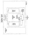
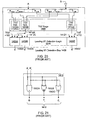
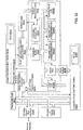
- execution unit 136C/D includes an input unit 210 which receives an add/subtract indication 202 and operands 204A-B.
- Input unit 210 is coupled an add/subtract pipeline 220, which includes a far data path 230 and a close data path 240.
- Far data path 230 and close data path 240 receive inputs from input unit 210 and generate far path result 232 and close path result 242, respectively, which are conveyed to a result multiplexer unit 250.
- Far data path 230 also conveys a select signal to multiplexer unit 250 in one embodiment.
- the select signal is usable to select either far path result 232 or close path result 242 to be conveyed as result value 252, which is the output of add/subtract pipeline 220.
- Input unit 210 receives the operand data, and conveys sufficient information to far data path 230 and close data path 240 to perform the add or subtract operation.
- add/subtract indication 202 is indicative of the operation specified by the opcode of a particular floating point arithmetic instruction. That is, add/subtract indication 202 corresponds to the opcode of an instruction being processed by unit 136C/D (a logic 0 may indicate an add opcode and a logic 1 a subtract opcode in one embodiment).
- Operands 204 are floating point numbers having sign, exponent, and mantissa portions according to a predetermined floating point format (such as IEEE standard 754).
- input unit 210 may be configured to make a determination whether effective addition or subtraction is occurring. (As described above, an subtract opcode value may effectively be an addition operand depending on the signs of operands 204). In one embodiment, input unit 210 determines whether inputs 202 and 204 represent effective addition or subtraction, and conveys outputs to far data path 230 and close data path 240. In an alternate embodiment, the determination of effective addition or subtraction is made prior to conveyance to unit 136C/D. Add/subtract indication 202 is thus reflective of either effective addition or subtraction, and sign bits of incoming operands 204 are adjusted accordingly. In yet another embodiment, the effective addition/subtraction determination may be made separately within far data path 230 and close data path 240.
- the format of the outputs of input unit 210 depends upon the format of unit 210 inputs and also the configuration of far data path 230 and close data path 240.
- unit 210 conveys the full sign, exponent, and mantissa values (S A , S B , E A , E B , M A , and M B ) of operands 204 to far data path 230, while conveying S A , S B , M A , M B , and two least significant bits of both E A and E B to close data path 240.
- the two least significant exponents bits are used for speculative determination of exponent difference (instead of a full subtract).
- far data path 230 and close data path 240 may receive input data of varying formats.
- Far data path 230 is configured to perform addition operations, as well as subtraction operations for operands having absolute exponent difference E diff which is greater than 1.
- Close data path 240 is configured to perform subtraction operations on operands for which E diff ⁇ 1.
- close data path 240 includes a selection unit which is configured to provide improved performance over prior art pipelines such as pipelines 10 and 30 described above.
- Far data path 230 and close data path 240 generate far path result 232 and close path result 242, respectively, which are both conveyed to result multiplexer unit 250. As shown, far data path also generates a select signal for unit 250, which is usable to select either input 232 or 242 as result value 252. In alternate embodiments of add/subtract pipeline 220, the select for multiplexer unit 250 may generated differently.
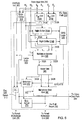
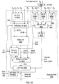
- far data path 230 receives an add/subtract indication, full exponent values (E A and E B ), and full mantissa values (M A and M B ) from input unit 210 in one embodiment.
- data path 230 also receives sign bits SA and S B , although they are not depicted in Fig. 6 for simplicity and clarity.
- Far data path 230 includes exponent difference calculation units 310A-B, which receive input exponent values E A and E B .
- Units 310 are coupled to right shift units 314A-B, which receive mantissa values M A and M B , respectively.
- Shift units 314 are also coupled to multiplexer-inverter unit 330 and logic unit 320 (referred to as "GRS" logic because unit 320 stores the guard (G), round (R), and sticky (S) bits shifted out in units 314).
- G guard
- R round
- S sticky bits shifted out in units 314.
- Multiplexer-inverter unit 330 in response to receiving shifted (316A-B) and unshifted versions of M A and M B , conveys a pair of operands (332A-B) to an adder unit 340.
- Adder unit 340 in turn, generates a pair of outputs 342A and 342B, which are conveyed to multiplexer-shift unit 360.
- Adder unit 340 is additionally coupled to a selection unit 350, which generates a select signal for multiplexer-shift unit 360.
- Selection unit 350 also receives inputs from exponent unit 310 and GRS logic unit 320 in addition to values from adder unit 340.
- select signal 352 conveyed from selection unit 350 multiplexer shift unit 360 conveys a mantissa value which, when coupled with an adjusted exponent value conveyed from an exponent adjust unit 370, is conveyed as far path result 232 to result multiplexer unit 250.
- Exponent adjust unit 370 receives the largest input exponent 309 (which is equal to max(E A , E B )) from an exponent comparator unit 308 coupled to receive E A and E B . Exponent 309 is additionally conveyed to close data path 240 for exponent calculations as is described below.
- exponent difference unit 310A is coupled to receive full exponent values E A and E B .
- Unit 310A is configured to compute the difference E B -E A and convey the resulting shift amount, 312A, to right shift unit 314A.
- Exponent difference unit 310B also receives full exponent values E A and E B , but is configured to compute the difference E A -E B , which is conveyed as shift amount 312B to right shift unit 314B.
- E A E B
- one of result 312 is negative (and therefore ultimately discarded by pipeline 220).
- An embodiment is also contemplated in which only one right shift unit 314 is provided; however, additional multiplexer logic may be needed to convey the proper mantissa value to the single shift unit. By providing two shift units 314, the performance of far data path 230 is increased.
- Shift amount 312A in one embodiment, is conveyed to a final select generation unit 311, along with add/subtract indication 202.
- Unit 311 in turn, generates an exponent difference select signal 313 to be conveyed to result multiplexer unit 250.
- the signal 313 generated by unit 310 is indicative of either far path result 232 or close path result 242.
- Signal 313 may thus be used by result multiplexer unit 250 to select either result 232 or result 242 as result value 252. If add/subtract indication 202 specifies an add operation, signal 313 is generated to be indicative of far path result 232.
- add/subtract indication 202 specifies a subtract operation and E diff (corresponding to the absolute value of shift amount 312A) is greater than one, signal 313 is also generated to be indicative of far path result 232. Conversely, if add/subtract indication 202 specifies a subtract operation and E diff is 0 or 1, signal 313 is generated to be indicative of close path result 242. In one embodiment, signal 313 may be used to cancel the far path result if E diff indicates result 242. E diff is also conveyed to selection unit 350 in one embodiment, as will be described below.
- Right shift units 314A-B generate shift outputs 316A-B, respectively, according to shift amounts 312A-B. These shift outputs are then conveyed to multiplexer-inverter unit 330.
- Unit 330 is also coupled to receive add/subtract indication from input unit 210 and the sign bit of shift amount 312A.
- multiplexer-inverter unit 330 is configured to swap operands 316A and 316B if operand 316B is determined to be greater than operand 316A. This determination may be made in one embodiment from the sign bit of shift amount 312A (or 312B). Additionally, unit 330 is configured to invert the smaller operand if subtraction is indicated by input unit 210. The outputs of unit 330 are conveyed to adder unit 340 as adder inputs 332A-B.
- GRS logic unit 320 receives values which are right-shifted out of units 314A-B. After shift amounts 312 are applied to values in shift units 314, GRS logic unit 320 generates guard, round, and sticky bits corresponding to the smaller mantissa value. As shown, these bit values are forwarded to selection unit 350 for the rounding computation.
- Adder unit 340 receives adder inputs 332A-B and generates a pair of output values 342A-B. Output 342A corresponds to the sum of input values 332 (sum), while output 342B corresponds to output 342A plus one (sum+1). Adder unit 340 also conveys a plurality of signals to selection unit 350, which generates and conveys select signal 352 to multiplexer-shift unit 360. Select signal 352 is usable to select either adder output 342A-B to be conveyed as the mantissa portion of far path result 232. By selecting either sum or sum+1 as the output of multiplexer-shift unit 360, the addition result may effectively be rounded according to the IEEE round-to-nearest mode.
- the exponent portion of far path result 232 is generated by exponent adjustment unit 370.
- Unit 370 generates the adjusted exponent from the original larger exponent value (either E A or E B ) and an indication of whether the adder output is normalized.
- the output of unit 370 is conveyed along with the output of unit 360 as far path result 232.
- Unit 330 includes a control unit 331 which receives shift amount 312A from exponent difference calculation unit 310A.
- Multiplexer-inverter unit 330 also includes a pair of input multiplexers 334A-B.
- Input multiplexer 334A receives unshifted mantissa values M A and M B
- multiplexer 334B receives shifted outputs 316A-B.
- the inputs to multiplexers 334 are configured such that control unit 331 may route a single control signal 333 to both multiplexer 334A and 334B.
- multiplexer 334B is inverted by an inverter 336 if a subtract operation is indicated by signal 202. If a subtract is indicated, a bit-inverted (one's complement) version of the output of multiplexer 334B is conveyed to adder 340 as adder input 342B. If an add operation is indicated by signal 202, inverter 336 is not enabled, and the output of multiplexer 334B is conveyed to adder unit 340 in non-inverted form.
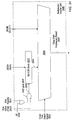
- Adder unit 340 includes adders 400A and 400B, each coupled to receive adder inputs 332A-B.
- Adder 400A is configured to generate adder output 342A (sum), while adder 400B is configured to generate adder output 342B (sum+1).
- adders 400A and 400B are each coupled to receive the sign and mantissa bits of operands 204A-B.
- adders 400 may be implemented using a variety of known adder types. For example, adders 400 may be implemented as ripple-carry adders, carry lookahead adders, carry-select adders, etc.
- adders 400 may combine features of different adder types.
- adders 400 compute the upper n/2 bits of their respective results in two different ways: that the carry in from the lower n/2 bits is 0, and that the carry in from the lower n/2 bits is 1.
- the use of Ling-style pseudo-carry may also be utilized in the lower n/2 bits to further reduce fan-in and gate delay.
- adder unit 340 may be implemented with just a single adder. This may be accomplished by recognizing that many of the terms computed in adders 400A-B are shared. Accordingly, both sum and sum+1 may be produced by a single adder. Although such an adder is larger (in terms of chip real estate) than either of adders 400, the single adder represents a significant space savings vis-a-vis the two adder configuration of Fig. 8.
- S MSB the most significant bit of the output of adder 400A
- select signal 352 the faster select signal 352 is generated, then, the faster result value 252 can be computed.
- S MSB is generated in selection unit 350 concurrently with the MSB computation performed in adder 400A.
- a MSB , B MSB , and C MSB the carry in to adder block 402B which generates S MSB ) are all conveyed to selection unit 350.
- the output of selection unit 350 may be generated more quickly, enhancing the performance of far data path 230.
- the two least significant bits of adder output 342A (S LSB+1 and S LSB ) are also conveyed to selection unit 350. In one embodiment, these values are not generated in parallel in unit 350 (in the manner of S MSB ) since the least significant bits are available relatively early in the addition operation (in contrast to more significant bits such as S MSB ).
- adder 400B operates similarly to adder 400A, except that carry in value 404B is a logical one. Since the carry in value (404A) for adder 400A is a logical zero, adder 400B generates a result equal to the output of adder 400A plus one. As will be described below, by generating the values (sum) and (sum+1) for a given pair of operands, the IEEE round to nearest mode may be effectuated by selecting one of the two values.
- selection unit 350 is shown in one embodiment of far data path 230. The general operation of selection unit 350 is described first, followed by examples of far path computations.
- selection unit 350 receives a plurality of inputs from adder unit 340. These inputs include, in one embodiment, the inputs to adder 400A block 402B (A MSB , B MSB , and C MSB ), the next-to-least significant bit (N) of adder output 342A, the least significant bit (L) of adder output 342B, and the guard (G), round (R), and sticky (S) bits from GRS logic unit 320. A logical-OR of the round and sticky bits, S 1 , is produced by logic gate 502. Bit S 1 is used for calculations in which R is not explicitly needed. Selection unit 350 also includes a selection logic block 510 which includes selection sub-blocks 510A-D.
- sub-blocks 510A-D In response to the inputs received from units 320 and 340, sub-blocks 510A-D generate respective select signals 512A-D. Select signals 512 are conveyed to a far path multiplexer 520, which also receives control signals including add/subtract indication 202, S MSB signal 534, and C S signal 536. S MSB signal 534 is conveyed from a multiplexer 530A, while C S is conveyed from a multiplexer 530B. In response to these control signals, multiplexer 520 conveys one of select signals 512 as far path select signal 352 to multiplexer-shift unit 360.
- adder unit 340 is configured to generate sum and sum+1 for operands 204A and 240B.
- Selection unit 350 is configured to generate far path select signal 352 such that the sum/sum+1 is a) corrected for one's complement subtraction and b) rounded correctly according to the IEEE round-to-nearest mode.
- a number generated by one's complement subtraction must have 1 added in at the LSB to produce a correct result.
- R, and S bits however, such correction may or may not be needed.
- sum+1 is selected in some instances to provide a result which is rounded to the next highest number.
- selection sub-blocks 510A-D speculatively calculate selection values for all possible scenarios. These selection values are conveyed to multiplexer 520 as select signals 512A-D. Control signals 302, 534, and 536 indicate which of the predicted select signals 512 is valid, conveying one of signals 512 as far path select signal 352.
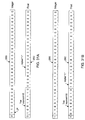
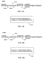
- FIG. 10A-B examples of addition accurately predicted by selection sub-block 510A are shown. Since sub-block 510A only predicts for addition, selection of sum+1 is used for rounding purposes only.
- Fig. 10A depicts an addition example 550A in which sum is selected. Rounding is not performed since G(L+S 1 ) is not true.
- Fig. 10B depicts an addition example 550B in which sum+1 is selected. Because G and S, are set, the result is closer to 1.01011 than to 1.01010. Accordingly, sum+1 (1.01011) is selected.
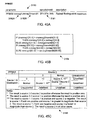
- Figs. 10C-10D examples of addition accurately predicted by selection sub-block 510B are shown. Since sub-block 510B only predicts for addition, selection of sum+1 is used for rounding purposes only.
- the examples shown in Figs. 10C-D are similar to those shown in Figs. 10A-B except that overflow conditions are present in examples 550C-D shown in Figs. 10C-D. Accordingly, the equation for selecting sum+1 is slightly different than for selection sub-block 510A.
- Fig. 10C depicts an addition example 550C in which sum is selected.
- Fig. 10D depicts an addition example 550D in which sum+1 is selected, effectively rounding up the result (after a 1-bit right shift to correct for overflow).
- Selection sub-block 510B selects sum+1 according to the equation L(N+G+S 1 ).
- Figs. 10E-F examples of addition accurately predicted by selection sub-block 510C are shown. Since sub-block 510C is used to predict selection for subtraction operations which have properly normalized results , selection of sum+1 is performed to correct for one's complement subtraction and for rounding purposes. As shown in example 550E, sum is indicated by select signal 512C since the guard and sticky bits are set before the subtract (ensuring that the result of the subtraction is closer to sum than sum+1). Conversely, in example 550F, the guard and sticky bits are both zero. Accordingly, a one-bit addition to the LSB is needed; therefore, sum+1 is selected. Generally speaking, selection sub-block 510C selects sum+1 according to the equation G'+LS 1 ', where G' and S 1 ' represent the complements of the G and S 1 bits.
- Figs. 10G-H examples of addition accurately predicted by selection sub-block 510D are shown. Since sub-block 510D is used to predict selection for subtract operations which require a 1-bit left shift of the result, selection of sum+1 is performed for both one's complement correction and rounding.
- sum is chosen as the result since both the guard and round bits are set before the subtract (ensuring that the result of the subtraction is closer to sum than sum+1). For this particular example, a zero is shifted into the LSB when the result is normalized. (In other examples, a one may be shifted in).
- both the guard and round bits are zero, which causes the result of the subtraction to be closer to sum+1 than sum. Accordingly, sum+1 is selected. A zero is shifted in at the LSB.
- selection sub-block 510D selects sum+1 according to the equation G'(R'+S'), while the shift value is generated according to the equation GR'+G'RS.
- selection unit 350 may also possible.
- the guard and round bit inputs may be inverted if the sticky bit is set, resulting in different rounding equations.
- Various other modifications to the selection logic are possible as well.
- multiplexer-shift unit 360 is depicted in one embodiment of far data path 230.
- multiplexer-shift unit 360 is coupled to receive adder outputs 342A-B and shift value 514.
- a concatenation unit 610 receives outputs 342 and shift value 514, and conveys shifted multiplexer outputs 604A-D to multiplexer 600.
- Multiplexer 600 receives signals 352 (far path select signal), 534 (S MSB ), and 536 (C MSB ) as control inputs. In response to these control signals, multiplexer 600 selects one of signals 342 or 604 as far path mantissa result 612.
- the exponent portion of far path result 232 is conveyed by exponent adjustment unit 370, which adjusts the original larger exponent value, in one embodiment, by the amount of normalization (or correction for overflow) required by the result.
- multiplexer 600 includes three groups of inputs, denoted as A, B, and C.
- Inputs A0 and A1 are adder outputs 342, representing sum and sum+1.
- Inputs B0 and B1 represent adder outputs 342 adjusted for overflow (a '0' is routed as the MSB by concatenation unit 610).
- inputs C0 and C1 represent adder outputs 342 after a one-bit left shift.
- Concatenation unit 610 utilizes the shift value conveyed from selection sub-block 510D to append as the LSB of the conveyed outputs 604C-D.
- signals 534 and 536 are usable to determine whether adder output 342A is normalized properly (input group A), has an overflow condition (input group B), or requires a one-bit left shift (input group C).
- Far path select signal 352 is then usable to determine which input within the selected input group is to be conveyed as far path mantissa result 612.
- close data path 240 is configured to perform effective subtraction operations for operands having an absolute exponent difference of 0 or 1. Subtraction operations with operands having other absolute exponent difference values (and all addition operations) are handled as described above in far data path 230.
- close data path 240 receives a variety of inputs from input unit 210.
- Close data path 240 includes an exponent prediction unit 704, which receives the two least significant exponent bits of exponents E A and E B .
- exponent prediction unit 704 generates a prediction 706 regarding the relationship of the full values of E A and E B .
- exponent prediction unit 704 only operates on the two least significant bits, the prediction may often be incorrect, due to differences in the upper order bits not considered by unit 704. For this reason, in one embodiment, the actual exponent difference is computed in far data path 230 and utilized as a final select signal to determine whether far path 230 or close path 240 includes the correct result value.
- Data path 240 further includes a shift-swap unit 710, which is coupled to receive an exponent prediction from unit 704, as well as mantissa values M A and M B from input unit 210. Shift-swap unit 710, in response to receiving the input mantissa values, generates shifted mantissa values 712A-B, which are conveyed to an adder unit 720. Unit 710 additionally generates a guard bit 714 which is conveyed to selection unit 730.
- Adder unit 720 is configured to generate a plurality of outputs (722A-B), representing sum and sum+1, respectively. Adder unit 720 also conveys a plurality of signals to selection unit 730 as will be described below.
- Selection unit 730 in response to receiving an exponent prediction from unit 704 and a plurality of control signals from adder unit 720 and shift-swap unit 710, generates a close path select signal 732, conveyed to a multiplexer-inverter unit 740.
- Signal 732 is usable to select either adder output 722A or 722B to be conveyed as close path preliminary result 742.
- Result 742 is conveyed to a left shift unit 750, which also receives a shift value from selection unit 730 and a predicted shift amount 772.
- Left shift unit 750 is configured to shift close path preliminary result 742 left by a number of bits indicated by shift amount 772.
- the shift value conveyed by selection unit 730 is shifted in at the LSB.
- the output of left shift unit 750 is the mantissa portion of close path result 242.
- the exponent portion of close path result 242 is generated by an exponent adjustment unit 780, which receives the largest input exponent value 309 from far data path 230.
- Unit 780 is configured to adjust exponent 309 by predicted shift amount 772 to produce the final close path exponent.
- the value of this exponent portion may be off by one in some cases due to the nature of the prediction mechanism. In one embodiment, this possible error is checked and corrected if needed in the final multiplexer stage.
- Predicted shift amount 772 is the output of a shift prediction unit 752.
- Unit 752 in one embodiment, is coupled to receive three sets of inputs at prediction units 754A-C.
- Prediction unit 754A is coupled to receive an unshifted version of mantissa value M A , and a negated version of M B which is right-shifted by one bit (this represents a prediction that operand 204A has an exponent value one greater than the exponent value of operand 204B).
- Prediction unit 754B is coupled to receive unshifted, non-negated versions of M A and M B , representing a prediction that the exponent values of both operands are equal.
- prediction unit 754C is coupled to receive an unshifted version of mantissa value M B and a negated version of M A which is right-shifted by one bit (representing a prediction that operand 204B has an exponent value one greater than the exponent value of operand 204A).
- the predictions of units 754A-C are concurrently conveyed to a shift prediction multiplexer 760, which receives an exponent prediction from unit 704 as a control signal.
- the output of shift prediction multiplexer 760 is conveyed to a priority encoder 770, which generates predicted shift amount 772.
- shift-swap unit 710 is coupled to receive exponent prediction value 706 from exponent prediction unit 704, as well as mantissa values M A and M B from input unit 210. Exponent prediction value 706 is conveyed to a pair of operand multiplexers 802A-B, as well as a guard bit generation unit 804.
- operand multiplexer 802A selects M B to be conveyed as a shift output 712A
- operand multiplexer 802B selects a one-bit-right-shifted version of M A to be conveyed as shift output 712B. Additionally, the bit shifted out of M A is conveyed as guard bit 714. (If exponent prediction value 706 predicts the exponents are not valid close path values, the output of shift-swap unit 710 is undefined in one embodiment since the far path result is selected in such a case).
- shift-swap unit 710 ensures that operand 712A is larger than operand 712B, the exponent difference for subsequent operations within close data path 240 is either 0 or 1 (-1 is no longer applicable).
- logic unit 810 is configured to receive exponent prediction value 706 and generate a corresponding exponent equality signal 812. As will be described below, exponent equality signal is utilized in selection unit 730 in order to generate close path select signal 732.
- close path 240 handles only subtraction operations, the output of multiplexer 802B, 712B, is inverted (one's complemented) before conveyance to adder unit 720.
- adder unit 720 includes a pair of adders units, 900A-B.
- Adder unit 900A receives shift outputs/adder inputs 712A-B and carry in signal 904A, and generates an adder output 722A.
- adder unit 900B receives shift outputs/adder inputs 712A-B and carry in signal 904B, and generates adder output 722B.
- Adder unit 720 generates outputs corresponding to sum and sum+1 by having carry in signal 904A at a logical zero and carry in signal 904B at a logical one.
- selection unit 730 generates a signal which selects either adder output 722A or 722B based upon a number of input signals.
- Adder unit 720 conveys a number of signals to selection unit 730 which are used in this calculation. These signals include sign bits A S and B S of operands 204, most significant bits A MSB and B MSB of operands 204, carry in signal 906 to MSB adder block 902B, and least significant bit S LSB of result 722A.
- adders 900A-B may be implemented as a single adder producing sum and sum+1.
- selection unit 730 receives a number of inputs in the embodiment shown, including least significant bit S LSB (L) from adder unit 720, guard bit (G) 714 from shift-swap unit 710, most significant bit B MSB , C MSB 906, and exponent equality signal 812, indicating whether exponents E A and E B are equal or differ by one.
- Selection unit 730 includes a selection logic block 950, which includes a plurality of selection sub-blocks 950A-D. Each sub-block 950A-D generates a corresponding select signal 952.
- Selection sub-block 950D also generates a shift value 954, which is conveyed to left shift unit 750.
- Select signals 952A-D are conveyed to a close path result multiplexer 960, which also receives a plurality of control signals. These control signals include exponent equality signal 812, an MSB value 956, and a sign value 958.
- MSB value 956 and sign value 958 are generated by a prediction select unit 962.
- prediction select unit 962 includes two multiplexers 970A-B. Multiplexer 970A is coupled to receive BMSB, and also has another input hardwired to receive a logic high signal. The output of multiplexer 970A, C S 957, is selected by C MSB 906. C S 957 is inverted by inverter 972 and conveyed as sign value 958, representing the sign of the output of adder unit 720. Multiplexer 970B, on the other hand, is configured to receive inverted and non-inverted versions of B MSB . C MSB also provides selection for multiplexer 970B. The output of 970B is conveyed to multiplexer 960 as the MSB of the output of adder unit 720.
- a separate zero detect unit may be utilized because in floating point representations such as IEEE standard 754, zero values are treated in a special fashion.
- a zero detect unit is not pictured in Fig. 15 for simplicity and clarity.
- Select signals 952A-D are conveyed to close path result multiplexer 960.
- the control signals also received by multiplexer 960 are usable to convey one of select signals 952 as close path select signal 732.
- these control signals for multiplexer 960 include, in one embodiment, exponent equality value 812, MSB value 956, and sign value 958.
- Exponent equality signal 812 is usable to determine whether close path select signal is one of signals 952A-B (equal exponents) or 952C-D (unequal exponents). If exponent equality signal 812 is indicative of equal exponents, sign value 958 is usable to determine whether adder output 722A is positive or negative. Accordingly, either signal 952A or 952B may be selected. Alternately, if exponent equality signal 812 is indicative of unequal exponents, MSB value 956 may be utilized to determine whether adder output 722A is properly normalized, allowing for selection of either signal 952C or 952D.
- MSB value 956 and sign value 958 are generated in parallel by selection unit 730. This allows close path select signal to be determined more quickly and speed operation of close data path 240.
- prediction selection unit 962 may also contemplated.
- C MSB signal 957 may be directly conveyed from adder unit 900A instead of being generated by prediction selection unit 960.
- unit 960 Various other embodiments of unit 960 are also possible.
- guard bit 714 is zero in this case, so borrowing is not performed.
- M B is larger than M A , however, the subtraction result is negative.
- actual result 1004A is the bit-inverted (one's complement) of computed result 1004B, which corresponds to adder output 722A.
- actual result 1004A may be computed by selecting adder output 722A for this case, inverting the resultant mantissa, and setting the sign bit ofthe result to indicate a negative number.
- adder output 722B (sum+1) is indicated by select signal 952C according to the equation G'.
- actual result 1006A is equal to computed result 1006B plus one. Accordingly, adder output 722B (sum+1) is selected.
- select signal 952C is indicative of adder output 722A (sum). This can be seen from the fact that actual subtraction result 1008A is equal to computed subtraction result 1008B.
- adder output 722B (sum+1) is indicated by select signal 952D according to the equation L+G'.
- a borrow is performed, canceling out the need for the one's complement correction.
- adder output 722A (sum) is selected by select signal 952D. This can be seen from the fact that actual subtraction result 1010A in Fig. 16E is equal to computed subtraction result 1010B.
- no borrow is performed in example 1000F, necessitating a one's complement correction of +1.
- adder output 722B (sum+1) is selected by select signal 952D. This can be seen from the fact that actual subtraction result 1010A in Fig. 16E is equal to computed subtraction result 1010B plus one.
- a borrow is performed from the LSB, cancelling the need for a one's complement correction of +1. Because both the LSB and guard bit are set in the result, however, the subtraction result is rounded up, according to an embodiment in which results are rounded to the nearest number (an even number in the case of a tie).
- adder output 722B is selected, effectively rounding the difference value to the nearest number (which is chosen to be the even number since the computed subtraction result 1014B is halfway between two representable numbers).
- Unit 740 is configured to select one of adder outputs 722 as close path preliminary result 742. Result 7412 is then conveyed to left shifter 750, described below with reference to Fig. 18.
- Multiplexer-inverter unit includes an AND gate 1106, a bit XOR block 1110, and a close path result multiplexer 1100.
- Bit XOR block 1110 is coupled to receive adder output 722A, as well as XOR enable signal 1108 from AND gate 1106.
- Bit XOR block 1110 in one embodiment, includes a two-input XOR gate for each bit in adder output 722A. One input of each XOR gate is a corresponding bit of output 722A; the other bit is XOR enable signal 1108.
- XOR block output 1104 is identical to adder output 722A. If signal 1108 is asserted, however, XOR block output 1104 is equal to the one's complement of adder output 722A. Signal 1108 is only enabled for the case in which the result of the close path subtraction is negative.
- close path result multiplexer 1100 In addition to receiving XOR block output 1104, close path result multiplexer 1100 also receives adder output 722B. Close path select signal 732, calculated in selection unit 730 as described above, is usable to select either output 1104 or 722B to be conveyed as close path preliminary result 742. Result 742 is then conveyed to left shift unit 750, described next with reference to Fig. 18.
- multiplexer-inverter unit 740 is configured to quickly perform the IEEE round-to-nearest operation.
- a result 742 is generated for forwarding to a normalization unit (left shifter).
- the value conveyed to the normalization unit of Fig. 18 is such that shifted output value is correctly rounded to the nearest number.
- This rounding apparatus advantageously eliminates the need to perform an add operation (subsequent to the add operation of adder unit 720) in order to perform rounding. Additionally, recomplementation is also achieved quickly since adder output 722A need only be inverted rather than having to perform a two's complement invert and add.
- left shift unit 750 includes a left shift register 1200 and a shift control unit 1210.
- Shift control unit 1210 receives predicted shift amount 772 from shift prediction unit 752 and shift value 954 from selection logic 950C. In response to these inputs, shift control unit 1210 controls the number of bits the value in register 1200 is shifted leftward. Shift control unit 1210 additionally controls what bit is shifted in at the LSB of register 1200 with each left shift. The result after shifting is conveyed as close path result 242.
- preliminary result 742 is either normalized or requires one or more bits of left shift for normalization. Furthermore, since the loss of precision due to operand alignment is at most one bit, only one value need be generated to shift in at the LSB. This value (shift value 954 in the embodiment shown) is shifted in at the LSB for the first left shift (if needed). If more than a one bit left shift is required, zeroes are subsequently shifted in at the LSB. The output of register 1200 is conveyed as close path result 242.
- result multiplexer unit 250 includes a final result shift control unit 1310, a 1-bit left shift unit 1312, a exponent correction adder 1313, and a pair of final multiplexers 1320.
- Final multiplexer 1320A selects to the exponent portion of result value 252, while final multiplexer 1320B selects the corresponding mantissa portion.
- Final multiplexer 1320A receives the exponent portions of both far path result 232 and close path result 242. Additionally, multiplexer 1320A receives the output of adder 1313, equal to the close path exponent plus one.
- predicted shift amount 772 is one less than the shift value needed to normalize the mantissa portion of close path 242. If this is the case, the close path exponent is one less than its true value. Accordingly, in addition the far and close path exponent values, the output of adder 1313 is also conveyed to multiplexer 1320A. Similarly, multiplexer 1320B receives far and close mantissa portions, along with a corrected close path mantissa value generated by shift unit 1312. The corrected close path mantissa value is generated for the case in which the mantissa of close path result 242 is not properly normalized. Guard bit 714 is shifted into the LSB in such a case.
- Shift control unit 1310 utilized exponent difference select 313 and close path MSB 1314 in order to generate final select signals 1322A-B.
- the actual exponent difference (calculated in far path 230) indicates whether far path result 232 or close path result 242 is to be selected.
- Exponent difference select 313 is thus used (along with signal 1314) to select one of the inputs to each of multiplexers 1320. If signal 313 indicates that the exponent difference is greater than one, far path result 232 exponent and mantissa portions are selected as result value 252.
- close path MSB 1314 selects whether the calculated or corrected versions of close path result 242 are conveyed as result value 252.
- shift prediction unit 752 includes three leading 0/1 prediction units 754.
- units 754A and 754C may be configured to provide improved speed and reduced space requirements.
- Fig. 20 a block diagram of a prior art leading 0/1 prediction unit 1400 is depicted.
- Prediction unit 1400 is configured to receive two operands and generate an indication of the location of the leading 0 (or 1) in the result value. As will be described below, the prediction generated by unit 1400 is accurate to within one bit position. The operation of prediction unit 1400 is described in order to provide a contrast to an improved leading 1 prediction unit described below with reference to Fig. 26.
- prediction unit 1400 includes a pair of operand input registers 1404A-B.
- Operand register 1404A receives operand A, storing bits A' MSB to A' LSB .
- Operand register 1404B receives a bit-inverted version of operand A, storing bits B' MSB to B' LSB .
- Prediction unit 1400 further includes a TGZ logic stage 1408, which includes TGZ generation units 1410A-1410Z.
- the TGZ generation unit which is coupled to A' LSB and B' LSB is denoted as "1410Z" simply to show that this unit is the final sub-block with logic stage 1408.
- the number of TGZ generation units 1410 within logic stage 1408 corresponds to the length of operands A and B).
- Each TGZ generation unit 1410 receives a pair of corresponding bits from operands A and B and produces, in turn, outputs T, G, and Z on a corresponding TGZ bus 1412.
- TGZ generation unit 1410A for example, produces T, G, and Z outputs on TGZ bus 1412A.
- Prediction unit 1400 further includes a leading 0/1 detection logic block 1418, which includes a plurality of sub-blocks 1420A-1420Z.
- Logic block 1418 typically includes either n or n+1 sub-blocks, where n is the number of bits in each of operands 1404.
- Each sub-block 1420 receives three TGZ bus 1412 inputs.
- a given logic sub-block 1420 has a corresponding TGZ generation unit 1410.
- TGZ generation unit 1410B for example, corresponds to logic sub-block 1420B.
- a given logic sub-block 1420 receives TGZ bus values from its corresponding TGZ generation unit, from the TGZ generation unit corresponding to the next most significant sub-block 1420, and from the TGZ generation unit corresponding to the next least significant sub-block 1420.
- logic sub-block 1420B receives TGZ bus 1412B from unit 1410B, TGZ bus 1412A from unit 1410A, and TGZ bus 1412C from unit 1410C. Unit 1410C is not pictured in Fig. 20).
- the first and last sub-blocks 1420 receive predefined TGZ values in one embodiment in order to handle the boundary cases.
- Each logic sub-block 1420 generates a prediction bit value 1430.
- Each value 1430 is usable to indicate the presence of leading 0 or 1 bits in its corresponding bit position. Collectively, values 1430A-Z make up leading 0/1 detection bus 1428.
- prediction unit 1400 may be optimized to reduce space requirements and increase performance. Such an improved prediction unit is described below with reference to Fig. 26. This prediction unit is particularly useful for speeding leading 1 predictions performed in close path 240 of add/subtract pipeline 220.
- Unit 1410 shown in Fig. 21 is representative of units 1410A-Z shown in Fig. 20.
- unit 1410 includes logic gates 1502A, 1502B, and 1502C, each of which receives inputs A' i and B' i , where i indicates a corresponding bit position within A and B.
- logic gate 1502A is an AND gate which generates an asserted value G i when both A' i and B' i are both true.
- Logic gate 1502B is an exclusive-OR gate which generates an asserted T i value if one of A' i and B' i is true.
- logic gate 1502C is a NOR gate which generates an asserted Z i value if A' i and B' i are both zero.
- the values G i , T i , and Z i make up TGZ bus 1412 for bit position i.
- the output of logic stage 1408 may be represented by a string of T's, G's, and Z's. It is known that a leading 1 may be predicted by matching the string T * GZ * , where the "*" may be read as "0 or more occurrences of”. Conversely, a leading 0 may be predicted by matching the string T*ZG*. As stated above, predictions generated by using these strings may be subject to a 1-bit correction.
- the actual leading 1 position is found in the third most significant bit position of the subtraction result.
- This operation is performed in hardware as A'+B', where A' is equal to A and B' is the inverted version of B.
- the resulting T-G-Z string is shown as TTGTT.
- This string stops matching the regular expression T * GZ * in the fourth most significant bit position.
- the leading 1 is thus indicated as being in the last bit position which matches the target string (the third most significant bit), which happens for this case to be the correct prediction.
- the actual leading 1 position is in the fourth most significant bit.
- the resulting T-G-Z string is TTGTZ.
- this string stops matching in the third most significant bit. This results in a leading 1 prediction which is off by one bit position.
- final result multiplexer 250 may be configured to correct this one-bit position error as described above.
- the leading 0 is found in the third most significant bit position.
- the resulting T-G-Z string is TZTGZ. This string stops matching the target string T * ZG * after the second bit position. This results in a leading 0 prediction which is off by one bit position.
- a logic diagram is shown for leading 0/1 detection sub-block 1420 (representative of sub-blocks 1420A-Z in Fig. 20). As shown, sub-block 1420 includes logic gate 1702A-C, 1704A-C, 1706, 1708, and 1710. An asserted prediction bit value 1430 indicates that either a leading 0 or leading 1 is present in this bit position.
- each of AND gates 1702 receives values from the current bit position, the previous bit position, and the next bit position.
- An assertion of one of gates 1702 indicates that the T-G-Z string produced by logic stage 1408 stops matching the target string T * GZ * in the next bit position.
- Each logic sub-block 1420 includes these gates 1702 in order to correspond to each of the possible ways a string match may end. It is noted that only one of the outputs of AND gates 1702 may be asserted at a given time. An assertion of one of the outputs of gates 1702 causes the output of gate 1706, leading 1 prediction 1707, to also be asserted.
- AND gates 1704A-C correspond to leading 0 detection in one embodiment.
- Each of these gates also receives TGZ values from the current bit position, the previous bit position, and the next bit position.
- An assertion of one of gates 1704 indicates that the T-G-Z string produced by logic stage 1408 stops matching the target string T * ZG * in the next bit position.
- Each of sub-blocks 1420 includes three gates in order to correspond to each of the possible ways a string match may end. It is noted that only one of the outputs of AND gates 1704 may be asserted at a given time.
- An assertion of any of the outputs of gates 1704 causes the output of OR gate 1708, leading 0 prediction 1709, to also be asserted.
- OR gate 1710 asserts signal 1430 if either of signals 1707 or 1709 is asserted. The most significant position within result bus 1430A-Z which is asserted indicates the position of the leading 0 or 1.
- sub-block 1420 is typically used when both leading 0 and 1 determination is to be performed. As such, this configuration is used in prediction unit 754B.
- prediction unit 1400 may be configured differently if more information is known regarding operands A and B.
- Sub-block 1800 is another embodiment of logic sub-block 1420 shown in Fig. 20.
- Sub-block 1800 is usable for operands with the restriction A>B.
- Sub-block 1800 receives T and Z values for each bit position in the sum of A'+B'.
- the T and Z values are coupled to inverters 1802A and 1802B, respectively.
- the outputs of inverters 1802, T i and Z i are coupled to an AND gate 1810, which conveys result bus 1820 as an output.
- Sub-block 1800 illustrates an improved method for generating leading 1 prediction when A>B. (Leading 0 prediction is not relevant since the result of subtraction is positive for A>B).
- the configuration of sub-block 1800 is accomplished noting that the leading 1 target string T * GZ * stops matching when the current bit position is not a T and the next bit position is not a Z.
- a prediction unit which includes sub-block 1800 for each bit may omit logic for generating G on a bit-by-bit basis, since this signal is not utilized in order to generate result bus 1820.
- FIG. 25 an illustration 1900 is shown depicting the derivation of an improved prediction unit 754A/C for close data path 240.
- operands in close data path 240 have an exponent difference E diff of either 0, +1, or -1.
- a prediction unit 754 which utilizes this detection technique is described with reference to Fig. 26.
- Unit 754A/C includes input registers 2000A-B. Input register 2000A receives operand A, storing bits A'MSB through A' LSB , while input register 2000B receives a bit-inverted version of operand B, storing bits B' MSB through B' LSB .
- Prediction unit 754A/C further includes a plurality of OR gates 2002A-Z, each coupled to receive a pair of input values from input registers 2000.
- the outputs of OR gates 2002 are conveyed to output register 2010.
- the collective output of register 2010 forms prediction string 2012.
- prediction bit value 2011Z is hardwired to a logic high value in order to produce a default leading 1 value.
- the prediction string 2012 generated by unit 754A/C is conveyed to shift prediction multiplexer 760.
- the contents of output register 2010 may be performed by using a single OR gate for each bit position.
- the first T-G-Z value of the result A'+B' is a G. (This results from A having an MSB of 1 and the inverted version of B, B', also having an MSB of 1).
- the result stops matching the target string of T * GZ * when Z is encountered in a bit position. Therefore, when the first Z value is detected at a particular bit position i, the prediction bit value 2011 for bit position i+1 (where i+1 is one bit more significant than position i) should indicate that a leading one value is present.
- Prediction bit value 2011A is asserted if either the second most significant bit of A' or the most significant bit of B' is set.
- bit values conveyed to OR gates 2002 from operand B' have a 1-bit relative bit position to those bit values conveyed from operand A'. This routing effectively performs the functionality of aligning A' and B'.
- B' may be shifted prior to conveyance to register 2000B. In such a case, the bit values routed to a particular gate 2002 would have common relative bit positions within input registers 2000). If either of these bits is set the second T-G-Z value in the result string is either G or T, but not Z.
- the strings stops matching in the second most significant bit position. This corresponds to a leading one being present in the most significant bit position.
- prediction bit value 2011A is asserted.
- the remaining prediction bit values 2011 are formed similarly.
- the final prediction bit value 2011Z is hardwired to a logical one (as a default in case none of the other bits are set). It is noted that although many bit values within prediction string 2012 may be asserted, typically only the most significant asserted position is utilized in determining the leading 1 position.
- each bit position includes an XOR gate (to generate T i ), a NOR gate (to generate Z i ), two inverters, and a final AND gate.
- Prediction unit 754A/C includes just a single OR gate for each bit position.
- each value within prediction string 2010 is generated using bit values from only a single bit position (two bits) in the input operands.
- far data path 230 and close data path 240 provides an efficient implementation of add/subtract pipeline 220 by eliminating operations not needed for each path.
- the versatility of add/subtract pipeline 220 may also be increased by expanding the pipeline to handle additional operations.
- Figs. 27-30 describe an embodiment of far data path 230 which is configured to perform floating point-to-integer conversions.
- Figs. 31-99 describe an embodiment of close data path 240 which is configured to perform integer-to-floating point conversions. As will be shown below, this additional functionality may be achieved with only a minimal number of hardware changes.
- a floating point number 2100 is shown (in single-precision IEEE format) along with its corresponding integer equivalent, integer number 2102. As shown, number 2100 is equal to 1.00111010011110100001101 x 2 16 . (The exponent field in number 2100 includes a bias value of +128). Integer number 2102 represents the integer equivalent of floating point number 2102, assuming a 32-bit integer format (with one bit designated as the sign bit). Accordingly, to convert floating point number 2100 to its integer equivalent, the floating point mantissa is shifted such that the most significant bit ofthe mantissa (in one embodiment, a leading "1" bit) ends up in the bit position representing the floating point exponent (16) in the integer format. As shown, depending on the value of the floating point exponent, not all bits of the floating point mantissa portion may be included in the integer representation.
- a floating point number 2200 is shown along with corresponding integer representation, integer number 2202. As shown, number 2200 is equal to -1.1 x 2 30 , with an implied leading "1" bit. Because the true exponent of floating point number 2200 (30) is greater than the number of mantissa bits (23+hidden 1), integer number 2202 includes all mantissa bits of the original number.
- Far data path 2300 is similar to far data path 230 described above with reference to Fig. 6; however, far data path 2300 is modified in order to perform floating point-to-integer (f2i) conversions.
- the components of far data path 2300 are numbered similarly to the components of far data path 230 in order to denote similar functionality.
- Exponent difference unit 2310A receives exponent values E B and E A as in far data path 230.
- Exponent difference unit 2310B receives the output of a multiplexer 2302 and exponent value E B , where E B corresponds to the floating point value which is to be converted to integer format.
- Multiplexer 2302 receives an exponent value E A and a maximum integer exponent constant, and selects between these two values based on an f2i signal 2304.
- signal 2304 is generated from the opcode of an float-to-integer conversion instruction. In the case of standard far path addition/subtraction, f2i signal 2304 is inactive, and E A is conveyed to exponent difference unit 2310B.
- multiplexer 2302 conveys the maximum integer exponent constant to exponent difference unit 2310B.
- the maximum integer exponent is indicative of the exponent of largest possible floating point value which may be converted to an integer (without clamping) by far data path 2300. If far data path 2300 is configured to handle the 32-bit signed integer format shown in Figs. 27A-B, the value 31 is used as the maximum integer exponent constant. In one embodiment, far data path 2300 may be configured to convert floating point numbers to different size integer formats. In such a case, a plurality of maximum exponent values may be multiplexed (selected by a size select signal) to provide the second input to multiplexer 2302.
- the entire data path is configured to handle max(m, n) bits, where m is the number of bits in mantissa values M A and M B , and n is the number of bits in the target integer format.
- far data path 2300 is wide enough to handle the largest possible data type for its defined operations.
- right shift units 314 are 32 bits wide.
- Shift units 314A-B receive mantissa values M A and M B , respectively, each of which is left aligned.
- Shift outputs 2316A-B are then conveyed to multiplexer-inverter unit 2330.
- Multiplexer-inverter unit 2330 receives shift outputs 2316, along with M A , M B , and an operand which is set to zero. (It is also noted that in another embodiment, mantissa value M A may itself be set to zero before conveyance to far data path 2300).
- Unit 2330 in response to receiving f2i signal 2304, is configured to convey the zero operand as adder input 2332A and the shifted version of M B as adder input 2332B.
- adder output 2342A is equal to adder input 2332B (M B ).
- Selection unit 2350 is thus configured to select adder output 2342A (sum) to perform the f2i operation.
- Adder unit 2340 produces sum and sum+1 outputs in response to the adder inputs. For f2i conversions, however, since one operand is zero, adder output 2342A is equal to adder input 2332B. Accordingly, selection unit 2350, in response to receiving f2i signal 2232, selects adder output 2342A (sum) within multiplexer-shift unit 2360.
- a multiplexer 2306 coupled between exponent adjust unit 2370 and multiplexer-shift unit 2360 is configured to provide the proper upper order bits for one embodiment of far path result 232.
- 24 bits (in one embodiment) of mantissa value are conveyed as the 24 least significant bits of result 232. Sign and exponent portions are conveyed as the upper order bits.
- f2i signal 2304 when f2i signal 2304 is inactive, the output of exponent adjust unit 2370 and a sign bit (not shown) is conveyed as the upper order bits of far path result 232.
- the upper order bits of adder output 2342A are conveyed as the upper order bits of far path result 232.
- far path result 232 includes one sign bit followed by 31 integer bits.
- floating point values above or below the maximum/minimum integer values are clamped to predetermined values.
- these maximum and minimum integer values are 2 31 -1 and -2 31 , respectively.
- FIG. 29 a block diagram of one embodiment of multiplexer-inverter unit 2330 is depicted.
- Unit 2330 is modified slightly from multiplexer-inverter unit 330 described above with reference to Fig. 7 in order to handle floating point-to-integer conversions.
- multiplexer-inverter unit 2330 includes control unit 2431, input multiplexers 2434A-B, and inverter 2436.
- Input multiplexer 2434A receives three inputs: M A , M B , and an zero operand set to zero, while input multiplexer 2434B receives the outputs 2316A-B of shift units 2314.
- Multiplexer 2434B receives another version of shift output 2316B as described below.
- adder unit 2340 During standard operation of far data path 2300, two 24-bit floating point mantissas are added by adder unit 2340. In order to accommodate 32-bit integer values, however, adder unit 2340 (and other elements of data path 2300) are 32 bits wide. Accordingly, the 24-bit M A and M B values are routed to the least significant 24 bits of the adder (with the upper order bits padded with zeroes) in order to perform addition and subtraction.
- control unit 2431 generates select signals 2433 such that multiplexer 2434A selects M A and multiplexer 2434B selects the 24-bit version of M B (shift output 316B). Conversely, for the case in which E B >E A , select signals 2433 are generated such that multiplexer 2434A selects M B and multiplexer 2434B selects the 24-bit version of M A (shift output 2316A).
- far data path 2300 performs the f2i function by adding zero to an appropriately shifted version of operand B, using the sum as the integer result. If f2i signal 2304 is active, control unit 2431 generates select signals 2433A-B so that the zero operand is selected by multiplexer 2434A as adder input 2332A and that the 32-bit version of shift output 2316B is selected by multiplexer 2434B. For the f2i instruction/function, inverter 2436 is inactive in one embodiment. Hence, the output of multiplexer 2434B is conveyed as adder input 2332B.
- the exponent value of the floating point number may often exceed the maximum representable integer value.
- the converted integer may be clamped at the maximum (or minimum) representable value to provide a usable result for subsequent operations.
- An example of result clamping for the f2i instruction is described below with reference to Fig. 30.
- result multiplexer unit 2500 is similar to multiplexer unit 250 depicted in Fig. 19, with additional hardware added to perform clamping of f2i conversion results.
- result multiplexer unit 2500 includes comparators 2504A-B, a shift control unit 2510, a left shift unit 2512, and a final multiplexer 2520.
- multiplexer 2520 is configured to select result value 252 from a plurality of inputs according to a final select signal 2522 generated by shift control unit 2510.
- Control unit 2510 generates select signal 2522 from exponent difference select 2313, comparator outputs 2504A-B, and the most significant bit of close path result 242 (denoted in Fig. 30 as numeral 2514).
- Exponent difference signal 2313 is indicative of either far path result 232 or close path result 242, with an additional indication of whether far path result 232 is an f2i result. If signal 2313 does indicate that far path result is an f2i result, comparator outputs 2506 indicate whether the f2i result should be clamped.
- far data path 2300 is similar to far data path 230, but with the additional f2i functionality. Because minimal hardware is needed to handle this extra instruction, the versatility of data path 2300 is increased with relativity little overhead. This provides an effective implementation of f2i conversion instructions through re-use of existing hardware. Similarly, integer-to-floating point conversion (i2f) may also be performed within add/subtract pipeline 220. One embodiment of pipeline 220 is described below with reference to Figs. 31-35 in which i2f conversions are performed in close data path 240.
- a 32-bit integer number 2550 is shown along with its corresponding IEEE single-precision equivalent 2552.
- the quantity represented by both numbers is 1.1 x 2 30 . Because the number of significant bits (2) in number 2550 is less than the number of mantissa bits in number 2552, no precision is lost. It is noted that in the embodiment shown, the mantissa portion of floating point number 2552 has a hidden 1 bit.
- a 32-bit integer number 2560 is shown along with its corresponding single-precision IEEE floating point equivalent 2562.
- integer 2560 includes more significant bits than are available in the mantissa portion of floating point number 2562. Accordingly, these extra bits are lost in the conversion process. It is noted that if the target floating point format includes a larger number of bits than are in the source integer format, no precision is lost during integer-to-float conversions.
- Close data path 2600 has a similar structure to that of close data path 240 described above with reference to Fig. 12, but data path 2600 is additionally configured to perform i2f conversions. The differences in functionality between data path 240 and data path 2600 are described below. Other embodiments are possible in which the leading 1 bit is explicit.
- i2f conversions are performed by setting operand A to zero. Accordingly, multiplexer 2601 receives both mantissa value M A and an operand set to zero. An i2f signal 2602 is utilized to select one of these input values to be conveyed as the output of multiplexer 2601. If i2f signal 2602 is inactive, mantissa value M A is conveyed to both shift-swap unit 2610 and prediction 2654B, in which case close data path 2600 operates identically to close data path 240. If i2f signal 2602 is active, however, the zero operand is conveyed to both units 2610 and 2654B.
- Shift-swap unit 2610 in response to receiving i2f signal 2602, selects 0 and M B to be conveyed as adder inputs 2620.
- close data path 2600 is only configured to perform subtraction.
- a positive integer input to close data path 2600 produces a negative result from adder unit 2620 (since the integer is effectively subtracted from zero).
- the "sum" output of adder 2620 may be inverted in order to produce the correct result.
- a negative integer input (in 2's complement form) to close data path 2600 produces a positive result from adder unit 2620.
- the 2's complement integer input is negated in shift-swap unit 2610 by taking the 1's complement. This results in an adder input having a magnitude which is one less than the original negative number. Accordingly, the correct output of adder unit 2620 is obtained by selecting the "sum+1" output, which corrects for the one's complement addition.
- selection unit 2630 selects the output of adder unit 2620 based on the sign of operand B if i2f signal 2602 is active. If an i2f instruction is being performed, adder output 2622A (sum) is chosen (and subsequently inverted) if the sign of operand B is 0 (indicating a positive number). On the other hand, adder output 2622B (sum+1) is chosen if the sign of operand B is 1 (indicating a negative number).
- Multiplexer-inverter unit 2640 in response to receiving close path select signal 2632, conveys the selected adder output 2622 as close path preliminary result 2642.
- Close path preliminary result 2642 is then normalized in left shift unit 2650 according to predicted shift amount 2672. If i2f signal 2602 is active, prediction unit 2654B receives a zero operand and a negated version of M B as inputs. The prediction string generated by unit 2654B is then selected by shift prediction multiplexer 2660 in response to signal 2602. Priority encoder 2670 then generates a predicted shift amount 2672 which is usable to left-align close path preliminary result within left shift unit 2650.
- left shift unit 2650 is an n+1 bit shifter, where n is the width of close data path 2600 (32 bits in one embodiment).
- the shifter is configured to be n+1 bits in order to account for the one bit position prediction error which may occur using the T-G-Z methodology for leading 0/1 detection. All n+1 bits may thus be conveyed to final multiplexer unit 2500. If the most significant bit is set (indicating proper normalization), the most significant n bits of the n+1 bits conveyed to unit 250 are selected as the mantissa portion of result value 252. Conversely, if the most significant bit is not set, the least significant n bits of the n+1 bits conveyed to unit 2500 are selected as the mantissa portion of result value 252.
- the exponent portion of close path result 242 is calculated by an exponent adjustment unit 2680 using either exponent large input 309 or the maximum exponent value for the given integer representation.
- the maximum exponent value is 31 in one embodiment. This corresponds to the largest exponent possible for an integer value within the given format.
- the operation of adjustment unit 2680 is described below with reference to Fig. 35.
- Fig. 33 a block diagram of one embodiment of shift-swap unit 2610 is depicted.
- Shift-swap unit 2610 is similar to unit 710 described above with reference to Fig. 13.
- Unit 2610 is additionally configured, however, to select the proper operands for the i2f operation.
- unit 2610 is coupled to receive i2f signal 2602.
- input multiplexers 2702A is configured to output the zero operand (conveyed as the output of multiplexer 2601) as adder input 2612A
- input multiplexer 2702B is configured to output operand M B .
- Operand M B is then negated by inverter 2708 and conveyed as adder input 2612B.
- Unit 2640 is similar in structure to unit 740 described above with reference to Fig. 17.
- Unit 2640 is additionally configured to provide proper selection for i2f conversions in addition to standard close path subtraction.
- unit 2640 is coupled to receive adder outputs 2622A-B.
- close path select signal 2632 selects of one of the adder inputs to be conveyed as close path preliminary result 2642.
- selection unit 2630 generates close path select signal according to the sign of the integer input number is i2f signal 2602 is active. If the i2f input is a positive number, close path select signal 2632 is generated to be indicative of adder output 2622A (sum). Because a positive i2f input in close path 2600 produces a negative output from adder 2620 in one embodiment, proper recomplementation is provided by inverting adder output 2622A in XOR block 2810. This produces a result of the correct magnitude which may be conveyed as close preliminary result 2642.
- exponent adjustment unit 2680 includes an exponent multiplexer 2902, an inverter 2904, a shift count adjustment multiplexer 29030, a half adder 2910, and a full adder 2920.
- Exponent adjustment unit 2680 is configured to subtract the predicted shift amount from an initial exponent in order to generate the exponent portion of close path result 242. In the case of standard close path subtraction (non-i2f operations), a correction factor is added back into the exponent to account for the difference in width between the integer and floating point formats. This function is described in greater detail below.
- close data path 2600 which is configured to handle a 32-bit integer format and a floating point format with a 24-bit mantissa portion.
- large exponent 309 is calculated within far data path 230 and conveyed to multiplexer 2902.
- predicted shift amount 2672 is calculated by shift prediction unit 2652 and conveyed to inverter 2904.
- the negated shift amount and large exponent 309 may then be added using half adder 2910 and full adder 2920.
- This adder configuration allows a correction constant conveyed from multiplexer 2930 to be added in as the second operand at bit 3 of full adder 2920.
- This correction constant is used since standard close path subtractions are over-shifted by 8 bits by left shift unit 2650.
- shift prediction unit 2652 is configured to generate predicted shift amounts for both integer and floating point values within data path 2600, the shift amounts are based on left-aligning both sets of values with the larger format, which in this embodiment is the 32-bit integer format.
- normalizing the floating point values produced by close path subtraction only requires the MSB of the subtraction result to be left aligned with a 24-bit field. In order to accommodate 32-bit integers, however, all close path results are left-aligned with a 32-bit field. Accordingly, the predicted shift amount minus 8 is subtracted from large exponent 309 in order to produce the adjusted exponent.
- the carry in to bit 0 of full adder 2920 is set in order to compensate for the one's complement addition of shift amount 2672.
- the exponent adjustment calculation is similar to that performed for standard close path subtraction. If i2f signal 2602 is active, however, the output of multiplexer 2902 is 31 and the correction constant conveyed from multiplexer 2930 is 0.
- i2f conversion in which the most significant bit of the adder output is located in bit 28 out of bits [31:0].
- the floating point number resulting from this integer is 1.xxx x 2 28 .
- the floating point exponent may thus be calculated by subtracting the shift amount (3) from the predetermined maximum integer exponent (31) without using a correction constant.
- exponent adjustment unit 2680 is shown in Fig. 35 as being implemented with half adder 2910 and full adder 2920, various other adder configurations are also possible to produce the exponent portion of close path result 242.
- the expansion of close data path 2600 to handle integer-to-floating point conversion also provides extra versatility to add/subtract pipeline 220.
- the additional functionality is included within data path 2600 with a minimum number of changes. Accordingly, i2f conversion capability is achieved with an efficient hardware implementation.
- the embodiments shown above depict a single add/subtract pipeline 220 within each of execution units 136C and 136D. These embodiments allow concurrent execution of floating point add and subtract instructions, advantageously increasingly floating point performance. By configuring pipelines 220 to handle integer-to-float and float-to-integer conversions as described above, execution units 136C-D may concurrently perform these operations as well.
- Performance may further be increased by configuring each of execution units 136C-D to include a plurality of add/subtract pipelines 220. As will be described below, this allows each of execution units 136C-D to perform vector operations (the ability the concurrently perform the same arithmetic/logical operations on more than one set of operands). This configuration also allows a number of other operations to be efficiently implemented by pipelines 220 at a small additional hardware cost. These instructions are particularly useful for the types of operations typically performed by units 136C-D.
- execution unit 136C/D is coupled to receive operands 204A-D and an instruction indication 3002, and includes input unit 3010 and add/subtract pipelines 220A-B.
- Each of pipelines 220 includes a far and close data path which is configured to operate as described above.
- the outputs of each pipeline 220 is selected by one of result multiplexers 250.
- the outputs of multiplexers 250 are conveyed as result values 3008A-B for storage in output register 3006.
- Instruction indication 3002 specifies which operation is performed concurrently in each pipeline 220. For example, if indication 3002 specifies an add operation, both pipelines 220 concurrently execute an add operation on operands 204.
- Pipeline 220A may add operands 204A and 204C, for instance, while pipeline 220B adds operands 204B and 204D. This operation is described in greater detail below.
- indication 3002 may specify any of the instructions described below with reference to Figs. 37-49.
- Additional operand instruction information specifies the input values by referencing one or more storage locations (registers, memory, etc.).
- add, subtract, float-to-integer, and integer-to-float conversion instruction may be performed in add/subtract pipeline 220 using far data path 230 and close data path 240.
- Vectored versions of these instructions for one embodiment of pipeline 220 are described below with reference to Figs. 37-42.
- the configuration of Fig. 36 with a plurality of pipelines 220 may additionally be expanded to handle a number of other vectored instructions such as reverse subtract, accumulate, compares, and extreme value instructions. Specific embodiments of such instructions are described with reference to Figs. 43-49. (Other embodiments of these instructions are also possible).
- PFADD instruction 3100 includes an opcode value 3101 and two operand fields, first operand field 3102A and second operand field 3102B.
- the value specified by first operand field 3102A is shown as being "mmregl", which, in one embodiment, maps to one of the registers on the stack of floating point execution unit 136E. In another embodiment, mmregl specifies a storage location within execution unit 136C or 136D or a location in main memory.
- second operand field 3102B is shown in one embodiment as either being another of the floating point stack registers or a memory location ("mmreg2/mem64"). Similarly, mmreg2 may also specify a register within execution unit 136C or 136D in another embodiment. As used in the embodiment shown in Fig. 36, operand fields 3102A-B each specify a pair of floating point values having a sign value, an exponent value, and a mantissa portion.
- a first vector portion (such as input value 204A in Fig. 36) of the value specified by first operand field 3102A is added to a first vector portion (e.g., 204C) of the input value specified by second operand field 3102B.
- this sum is computed within far path 230A of pipeline 220A.
- this sum is then written back to the upper portion of operand 3102A (mmregl[63:32]).
- a destination storage location may be specified which is different than either of the source operands.
- PFADD instruction 3100 also specifies that a second vector portion of the input value specified by first operand field 3102A (e.g., 204B) is added to a second vector portion (e.g., 204D) of the input value specified by second operand field 3102B. This sum is computed in far data path 230B of add/subtract pipeline 220B. This sum is then written, in one embodiment, to the lower portion of the location specified by operand 3102A (mmregl[31:0]), although an alternate destination location may be specified in another embodiment. In one embodiment, the two add operations specified by instruction 3100 are performed concurrently to improve performance.
- PFSUB floating-point vectored subtract instruction
- the format of PFSUB instruction 3110 is similar to that described above for PFADD instruction 3100.
- PFSUB instruction 3110 includes an opcode value 3111 and two operands, first operand field 3112A and second operand field 3112B.
- the value specified by first operand field 3112A is shown as being "mmregl", which, in one embodiment, maps to one of the registers on the stack of floating point execution unit 136E. In another embodiment, mmregl specifies a register or storage location within execution unit 136C/D.
- second operand field 3112B is shown, in one embodiment, as either being another of the floating point stack registers or a memory location ("mmreg2/mem64"). Similarly, mmreg2 may also specify a register within execution unit 136C/D in another embodiment. As with PFADD instruction 3100, the values specified by operand fields 3112A-B for PFSUB instruction 3110 each specify a pair of floating point numbers each having a sign value, an exponent value, and a mantissa portion.
- a first vector portion (such as input value 204C shown in Fig. 36) of the input value specified by second operand field 3112B is subtracted from a first vector portion of the value (e.g., value 204A) specified by first operand field 3112A.
- this difference may be computed in either far path 230A or close path 240A of pipeline 220A depending on the exponent difference value between the operands.
- this difference value is written back to the upper portion of the value specified by first operand field 3112A (mmregl[63:32]), although an alternate destination may be specified in other embodiments.
- PFSUB instruction 3110 also specifies that a second vector portion (such as value 204D) of the value specified by second operand field 3112B be subtracted from a second vector portion (e.g., 204B) of the input value specified by first operand field 3112A. This difference is written to the lower portion of operand 3112B (mmregl[31:0]) in one embodiment, but may be written to another location in other embodiments. In a configuration such as that shown in Fig. 36, both difference calculations are performed concurrently in respective add/subtract pipelines 220 to improve performance.
- PF2ID vectored floating point-to-integer conversion instruction
- the format of PF2ID instruction 3120 is similar to those described above.
- PF2ID instruction 3120 includes an opcode value 3121 and two operand fields, first operand field 3122A and second operand field 3122B.
- the value specified by first operand field 3122A is shown as being "mmregl", which, in one embodiment, maps to one of the registers on the stack of floating point execution unit 136E. In another embodiment, mmregl specifies a register or storage location within one of execution units 136C-D.
- mmregl specifies a destination location for the result of instruction 3120.
- the value specified by second operand field 3122B is shown as either being another of the floating point stack registers or a memory location ("mmreg2/mem64"). (Operand field 3122B may also specify a register or storage location within one of execution units 136C-D). Operand field 3122B specifies a pair of floating point numbers having a sign value, an exponent value, and a mantissa portion. It is noted that instruction 3120 produces a pair of 32-bit signed integer values in the embodiment shown. A floating point-to-integer instruction which produces a pair of 16-bit signed integers is described below with reference to Figs. 40A-C.
- PF2ID instruction 3120 operates separately on the first and second floating point numbers specified by second operand field 3122B. If the first floating point number specified by operand 3122B is outside the allowable conversion range, the corresponding output value is clamped at either the maximum or minimum value. If the first floating point input value is within the allowable input range, a float-to-integer conversion is performed in far data path 220A as described above. In one embodiment, the resulting integer is written to the upper portion of the storage location specified by operand field 3122A. This storage location may map to a floating point register within execution unit 136E, or may alternately be located within execution unit 136C/D or in main memory.
- Pseudocode 3124 also specifies a similar conversion process for the second floating point input value specified by operand field 3122B. This floating point number is converted to a signed 32-bit integer and written to the upper half of the storage location specified by operand field 3122A in one embodiment. If microprocessor 100 is configured to include a plurality of add/subtract pipelines 220, the second f2i conversion may be performed in add/subtract pipeline 220B concurrently with the first conversion to improve performance.
- a table 3128 is given illustrating the integer output values resulting from various floating point input values. It is noted that the f2i conversion process truncates floating point numbers, such that the source operand is rounded toward zero in this embodiment.
- PF2IW instruction 3130 includes an opcode 3131 and a pair of operands fields 3132A-B.
- Fig. 40-B gives pseudocode 3134 which describes the operation of PF2IW instruction 3130.
- Instruction 3130 operates in a similar fashion to instruction 3120 except that the target integers are signed 16-bit integers rather than signed 32-bit integers. The maximum and minimum values for instruction 3130 reflect this change.
- the f2i conversions are performed in far data paths 230A-B in the configuration of execution unit 136C/D shown in Fig. 36.
- Table 3138 shown in Fig. 40C illustrates the output values of instruction 3130 for various ranges of input values.
- Instruction 3140 includes an opcode value 3141 and a pair of operand fields 3142A-B.
- instruction 3140 is usable to convert a pair of signed 32-bit integers (specified by operand field 3142B) to a pair of corresponding floating point numbers (specified by operand field 3142A).
- instruction 3140 may be used to convert floating point numbers of other sizes.
- instruction 3140 performs integer-to-float conversions on each of the values specified by operand field 3142B.
- execution unit 136C/D shown in Fig. 36 each of the conversions may be performed concurrently within close data paths 240A-B of add/subtract pipelines 220A-B.
- instruction 3150 includes an opcode value 3151, and a pair of operand fields 3152A-B.
- the source values are a pair of floating point numbers specified by operand field 3152B.
- Pseudocode 3154 given in Fig. 42B illustrates the operation of instruction 3150.
- Instruction 3150 operates similarly to PI2FD instruction 3140 described above with reference to Figs. 41A-B, but instruction 3150 converts a pair of 16-bit signed integers to corresponding floating point values. In one embodiment, these floating point output values are written to respective portions of the storage location specified by operand field 3152A.
- Execution unit 136C/D shown in Fig. 36 is configured to handle vectored add, subtract, f2i, and i2f instructions as described above.
- pipelines 220A-B may be enhanced to handle additional vectored instructions as well.
- These instructions include, but are not limited to, additional arithmetic instructions, comparison instructions, and extreme value (min/max) instructions. These instructions may be realized within pipelines 220 with relatively little additional hardware, yielding an efficient implementation. Specific embodiments of such instructions are described below with reference to Figs. 43-49, although other instruction formats are possible in other embodiments.
- PFACC instruction 3160 includes an opcode value 3161 and two operand fields, first operand field 3162A and first operand field 3162B.
- First operand field 3162A (“mmregl") specifies a first pair of floating point input values in one embodiment.
- Operand field 3162A may specify a location which maps to one of the registers on the stack of floating point execution unit 136E.
- operand field 3162A specifies a register or storage location within execution unit 136C/D.
- Second operand field 3162B (“mmreg2") specifies a second pair of floating point input values. These input values may be located on the floating point stack of unit 136E or within a storage location in execution unit 136C/D.
- Fig. 43B pseudocode 3164 illustrating operation of instruction 3160 is shown.
- Accumulate instruction 3160 is slightly different than other floating point vector operations described above (such as PFADD instruction 3100 and PFSUB instruction 3110).
- instructions 3100 and 3110 operate on corresponding parts of two different register values to produce an output value.
- PFADD instruction 3100 forms a first portion of a vector output value by adding a first vector portion of a first input register to a first vector portion of a second input register.
- PFACC instruction 3160 adds the component values of each floating point input register separately. As shown in Fig.
- the first portion of the vector output value produced by instruction 3160 is equal to the sum of the pair of floating point input values within the storage location specified by first operand field 3162A. This addition operation is performed within far data path 230A of add/subtract pipeline 220A. The second portion of the vector output value for instruction 3160 is produced similarly within far data path 230B of add/subtract pipeline 220B.
- PFACC instruction 3160 operates on vectored components of a single input storage location, this instruction is particularly advantageous in matrix multiply operations. Matrix multiply operations may be effectuated by performing vector multiply operations, then summing the resulting values to obtain a sum of products. It is noted that PFACC instruction 3160 provides an advantageous means for summing the result of these vector multiply operations, particularly if these results reside in a single vector register. Because matrix multiply operations are quite prevalent in 3-D graphics operations, the use of instruction 3160 may significantly increase the graphics processing capabilities (particularly with regard to front-end geometry processing) of a system which includes microprocessor 100.
- PFSUBR floating-point vectored reverse subtract instruction
- the format of PFSUBR instruction 3170 is similar to that described above for PFSUB instruction 3110.
- PFSUBR instruction 3110 includes an opcode value 3171 and two operands, first operand field 3172A and second operand field 3172B.
- the floating point input values specified by operand fields 3172A-B may map to the stack of floating point unit 136E in one embodiment. These values may additionally be located within a register or storage location within execution unit 136C/D.
- PFSUBR instruction 3170 portions of the values specified by operand field 3112B are subtracted from corresponding portions of the values specified by operand field 3112A. Conversely, in PFSUBR instruction 3170, portions of the values specified by operand field 3172A are subtracted from the corresponding portions of the values specified by operand field 3172B.
- a first vector portion (such as input value 204A) of the value specified by first operand field 3172A is subtracted from a first vector portion (e.g., 204C) of the value specified by second operand field 3172B.
- This subtraction operation may either be performed within far data path 230A or close data path 240A depending upon the exponent difference value of the operands.
- this difference value is written back to the upper portion of operand 3172A (mmregl[63:32]). In other embodiments, the difference value may be written back to a different destination storage location.
- a second vector portion of the value specified by first operand field 302A is subtracted from a second vector portion of the value specified by second operand field 302B.
- This difference is written, in one embodiment, to the lower portion of the location specified by operand 302A (mmregl [31:0]).
- this second reverse subtract operation is performed either in far data path 230B or close data path 230B of add/subtract pipeline 220B.
- extreme value functions are those functions which return as a result either a maximum or minimum value selected among a plurality of values.
- a minimum value or a maximum value is obtained through the execution of several sequentially executed instructions. For example, a compare instruction may first be executed to determine the relative magnitudes of a pair of operand values, and subsequently a conditional branch instruction may be executed to determine whether a move operation must be performed to move the extreme value to a destination register or other storage location.
- These sequences of commands commonly occur in multimedia applications, such as in clipping algorithms for graphics rendering systems. Since extreme value functions are implemented through the execution of multiple instructions, however, a relatively large amount of processing time may be consumed by such operations. Graphics processing efficiency may be advantageously increased by dedicated extreme value instructions as described below with reference to Figs. 45-46.
- PFMAX instruction 3180 includes an opcode value 3181 and two operands, first operand field 3182A and first operand field 3182B.
- the value specified by first operand field 3182A is shown as being "mmregl", which, in one embodiment, is one of the registers on the stack of floating point execution unit 136E.
- the storage locations specified by operand field 3182A may be located in alternate locations such as execution unit 136C/D.
- second operand field 3182B may also specify the floating point stack registers, a memory location, or a register within unit 136C/D.
- second operand field 3182B specifies an immediate value.
- Fig. 45B pseudocode illustrating operation of PFMAX instruction 3180 is given.
- a comparison of a first vector portion (such as value 204A) of the value specified by first operand field 3182A and a first vector portion of the value specified by second operand 3182B (e.g., 204C) is performed upon execution of PFMAX instruction 3180.
- a comparison of a second vector portion (such as value 204B) of the value specified by first operand field 3182A and a second vector portion of the value specified by second operand field 3182B (e.g., 204D) is also performed.
- first vector portion of the value specified by first operand field 3182A is found to be greater than the first vector portion of the value specified by second operand field 3182B, the value of the first vector portion of the value specified by first operand field 3182A is conveyed as a first portion of a result of instruction 3180. Otherwise, the value of the first vector portion of value specified by second operand field 3182B is conveyed as the first vector portion of the result of instruction 3180.
- the second vector portion of the result of the PFMAX instruction is calculated in a similar fashion using the second vector portions of the values specified by operands fields 3182A-B.
- Table 3188 depicts the output of instruction 3180 for various inputs.
- Table 3188 includes cases in which operands 3182 are set to zero or in unsupported formats.
- Figs. 46A-C the format and operation of a vectored floating point (“PFMIN") instruction 3190 is shown.
- instruction 3190 includes an opcode value 3191, and a pair of operands fields 3192A-B.
- Operation of PFMIN instruction 3190 is similar to that of PFMAX instruction 3180, although instruction 3190 performs a minimum value function instead of a maximum value function.
- the operation of instruction 3190 is given by pseudocode 3194 in Fig. 45B.
- Fig. 45C includes a table 3198 which illustrates outputs of PFMIN instruction 3190 for various input values, including zero values and unsupported formats.
- vectored extreme value functions such as PFMAX instruction 3180 and PFMIN instruction 3190 are particularly useful for performing certain graphics processing functions such as clipping. Because the operands in extreme value functions are compared in order to produce a result value, vectored comparison instructions may also be realized within an execution unit 136C/D which is configured to perform extreme value instructions 3180 and 3190. Three such comparison instructions are described below with reference to Figs. 47-49.
- PFCMPEQ instruction 3200 includes an opcode value 3201 and two operands, first operand field 3202A and first operand field 3202B.
- the value specified by first operand field 3202A is shown as being "mmreg1", which, in one embodiment, is one of the registers on the stack of floating point execution unit 136E.
- First operand field 3202A may also specify a register or storage location within execution unit 136C/D.
- second operand field 3202B, "mmreg2" is shown as either being another of the floating point stack registers or a memory location.
- second operand field 3202B specifies an immediate value or a register/storage location within unit 136C/D.
- Fig. 47B pseudocode 3204 illustrating operation of PFCMPEQ instruction 3200 is given.
- a comparison of a first vector portion (such as value 204A) of the value specified by first operand field 3202A and a first vector portion of the value second operand 3202B (e.g., 204C) is performed upon execution of PFCMPEQ instruction 3200.
- a comparison of a second vector portion (e.g., 204B) of the value specified by first operand field 3202A and a second vector portion of the value specified by second operand field 3202B (204D) is also performed.
- first mask constant is conveyed as a first portion of a result of instruction 3200.
- this first mask constant is all 1's (FFFF_FFFFh), but may be different in other embodiments.
- a second mask constant 0000_0000h in one embodiment is conveyed as the first vector portion of the result of instruction 3200.
- Fig. 47C is a table which shows the output of instruction 3200 given various inputs, including cases in which operands 3202 are zero or in unsupported formats.
- the result (both the first and second vector portions) of instruction 3200 is subsequently written to the storage location specified by operand field 3202A.
- the result value may be stored to mmreg2, a memory location, or a third register specified by an additional operand. It is noted that in other embodiments of operands 3202, these values may include additional vector values beyond the two vector values shown in Fig. 47A.
- Figs. 48A-C the format and operation of a vectored floating point greater than compare operation (“PFCMPGT") instruction 3210 is shown.
- instruction 3210 includes an opcode value 3211, and a pair of operand fields 3212A-B.
- Instruction 3210 is performed in a similar fashion to instruction 3200, although a greater than comparison test is performed instead of an equality test.
- the operation of PFCMPGT instruction 3210 is given by pseudocode listing 3214 in Fig. 48B.
- Fig. 48C includes a table 3218 which gives outputs for various input values of instruction 3210.
- Figs. 49A-C the format and operation of a vectored floating point greater than or equal compare operation (“PFCMPGE") instruction 3220 is shown.
- instruction 3220 includes an opcode value 3221, and a pair of operand fields 3222A-B.
- Instruction 3220 is performed in a similar fashion to instructions 3200 and 3210, although instruction 3220 effectuates a greater than or equal to comparison test.
- the operation of PFCMPGE instruction 3220 is given by pseudocode listing 3224 in Fig. 49B.
- Fig. 49C includes a table 3228 which gives outputs for various input values of instruction 3220.
- execution unit 136C/D includes a pair of add/subtract pipelines 220A-B with respective far and close data paths for performing add, subtract, f2i, and i2f instructions as described above.
- the embodiment of execution unit 136C/D shown in Fig. 50 additionally includes an input unit 3310 and an output unit 3320 which allow implementation of a number of other instructions, particularly those described above with reference to Figs. 37-49.
- execution unit 136C/D is coupled to receive inputs into a pair of input registers 3304A-B.
- each register 3304 is configured to store a first vector value and a second vector value.
- input register 3304A is configured to store first vector portion 204A and second vector portion 204B.
- input register 3304B is configured to store first vector portion 204C and second vector portion 204D.
- these registers may include either integer or floating point values depending upon the type of operation being performed.
- Instruction indication 3302 may specify any number of operations, including those described above (add/subtract, accumulate, f2i, i2f, extreme value, compare). For the embodiment of execution unit 136C/D shown in Fig. 50, all of the instructions described above are performed. In alternate embodiments, a unit 136C/D may only execute a subset of these instructions. In still other embodiments, execution unit 136C/D may also execute additional instructions to those described above (a vectored floating point instruction which performs a less than comparison test, for example).
- input unit 3310 is configured to route the appropriate combination of operand values 204 to add/subtract pipelines 220A-B via operand buses 3012A-D.
- Each data path within each of pipelines 220A-B receives an "A" operand value and a "B" operand value, even if one or more of these values is not utilized within a particular data path.
- an f2i instruction is performed in the far data path 230A of pipeline 220A in one embodiment. Accordingly, the values conveyed to close data path 230B in pipeline 220A are not utilized for that particular instruction.
- different portions of the A and B operands may be conveyed to data paths 230 and 240.
- far data paths 230A-B receive full exponent values
- close data paths 240A-B receive only the two least significant bits of each exponent for performing leading 0/1 prediction.
- instruction indication 3302 may indicate an effective operation (e.g., effective addition or subtraction) rather than an explicit operation denoted by an opcode.
- Add/Subtract Pipeline 220A Add/Subtract Pipeline 220B Op A Op B Op A Op B PFADD A 1 B 1 A 0 B 0 PFSUB A 1 B 1 A 0 B 0 PFSUBR A 0 B 0 A 1 B 1 PFACC A 1 A 0 B 1 B 0 PF2ID, PF2IW - B 1 - B 0 PI2FD, P12FW - B 1 - B 0
- far data paths 230A-B and close data paths 240A-B operate substantially as described above.
- Far data paths 230A-B perform effective addition, as well as effective subtraction for operands with E diff >1.
- close data paths 240A-B perform effective subtraction on operands with E diff ⁇ 1.
- Each pipeline 220 selects its corresponding far path result 232 or close path result 242 to be conveyed as result value 252.
- Pipeline 220A generates result value 252A
- pipeline 220B generates result value 252B.
- Result values 252A-B are conveyed to output unit 3320 and utilized as described below to generate output values 3008A-B.
- output unit 3320 is coupled to receive a maximum integer value 3321, a minimum integer value 3322, first and second mask constants 3324A-B, and operands 204A-D (A 1 , A 0 , B 1 , and B 0 ).
- Output unit 3320 includes clamping comparators 3030A-D, extreme value comparator 3340, output selection logic 3350, and output multiplexer 3360.
- Output multiplexer 3360 is configured to convey output values 3008A-B to output register 3006.
- Result values 252A-B convey output values for add, subtract, f2i, i2f, and accumulate instructions.
- Maximum integer value 3321 and minimum integer value 3322 are used for clamping f2i instruction results if needed.
- Operand values 204A-D are used to generate the output of the extreme value (min/max) instructions.
- First and second mask constants 3324A-B are used as outputs of the comparison instructions such as the equality compare, greater than compare, and greater than or equal to compare instructions described above.
- output selection logic 3350 may be used to select the appropriate multiplexer 3360 inputs to be conveyed as output values 3308A-B. It is noted that because of the vector nature of the input and output registers of execution unit 136C/D, output multiplexer 3360 accordingly selects a pair of output values. Accordingly, multiplexer 3360 is shown in Fig. 50 as having sub-portion 3360A (configured to convey output 3308A) and sub-portion 3360B (configured to convey output 3308B). Output selection logic 3350 generates a pair of corresponding select signals, 3352A-B, to control each of these multiplexer sub-portions.
- Output selection logic receives instruction indication 3302, the outputs of clamping comparators 3030A-D, and the output of extreme value comparator 3340. If instruction indication 3302 specifies that an arithmetic instruction is being performed, result values 252A-B are conveyed as output values 3008A-B to output register 3006.
- result values 252A and 252B (calculated in far data paths 230A-B, respectively) are conveyed as output values 3008A-B unless one or both values exceed maximum integer value 3321 or minimum integer value 3322.
- Overflow and underflow conditions are detected by clamping comparators 3330A-D and conveyed to output selection logic 3350.
- the maximum and minimum integer values are conveyed as output values 3008 in place of the values which caused the overflow/underflow condition.
- the f2i instruction specified by indication 3302 may generate integers of a variety of sizes as described above.
- result values 252A and 252B are conveyed as output values 3008A-B. It is noted that in the embodiment shown, the dynamic range of the floating point format exceeds the maximum and minimum integer values, so overflow/underflow detection logic is not used for the i2f instruction.
- the i2f instruction may specify conversion of integers of a variety of sizes as described above.
- extreme value comparator 3350 If an extreme value instruction is indicated by instruction indication 3302, extreme value comparator 3350 generates a plurality of outputs usable to determine the maximum and minimum values from each input pair. For example, if instruction indication 3302 specifies a maximum value instruction, comparator 3350 tests whether operand 204A is greater than operand 204C. If operand 204A is greater, it is conveyed as output value 3008A. Otherwise, operand 204C is conveyed.
- comparator 3350 The outputs generated by comparator 3350 are also usable to implement the comparison instructions described above. If a comparison instruction is specified by indication 3302, comparator outputs 3350 determine whether first or second mask constant 3324 is conveyed for each output value 3008. It is noted that different mask constants may be generated for each portion of output register 3006 depending upon the particular input values in question.
- execution units 136C/D shown above provide an efficient means for performing floating point arithmetic operations such as add and subtract.
- the improved selection logic implemented in one embodiment of close path 240 results in an add/subtract pipeline 220 with only one full add and one full shift in each of data paths 230 and 240.
- data paths 230 and 240 may additionally be configured to perform floating point-to-integer and integer-to-floating point conversions with little additional hardware. Such a capability is particularly important for an embodiment of execution unit 136C/D which handles both integer and floating point data (which may or may not be vectored).
- vectored floating point instructions may be performed. This capability is advantageous in applications such as geometry processing for graphics primitives, in which identical operations are performed repetitively on large sets of data.
- each of units 136C-D with a pair of add/subtract pipelines 220, up to four vectored floating point operations may be performed concurrently in microprocessor 100.
- execution unit 136C/D may be expanded to handle additional arithmetic operations such as reverse subtract and accumulate functions.
- proper output multiplexing allows execution unit 136C/D to accommodate additional instruction such as extreme value and comparison instructions.
- a block diagram of one embodiment of a computer system 3400 including microprocessor 100 coupled to a variety of system components through a bus bridge 3402 is shown.
- a main memory 3404 is coupled to bus bridge 3402 through a memory bus 3406
- a graphics controller 3408 is coupled to bus bridge 3402 through an AGP bus 3410.
- a plurality of PCI devices 3412A-3412B are coupled to bus bridge 3402 through a PCI bus 3414.
- a secondary bus bridge 3416 may further be provided to accommodate an electrical interface to one or more EISA or ISA devices 3418 through an EISA/ISA bus 3420.
- Microprocessor 100 is coupled to bus bridge 3402 through a CPU bus 3424.
- Bus bridge 3402 provides an interface between microprocessor 100, main memory 3404, graphics controller 3408, and devices attached to PCI bus 3414.
- bus bridge 3402 identifies the target of the operation (e.g. a particular device or, in the case of PCI bus 3414, that the target is on PCI bus 3414).
- Bus bridge 3402 routes the operation to the targeted device.
- Bus bridge 3402 generally translates an operation from the protocol used by the source device or bus to the protocol used by the target device or bus.
- secondary bus bridge 3416 may further incorporate additional functionality, as desired.
- secondary bus bridge 3416 includes a master PCI arbiter (not shown) for arbitrating ownership of PCI bus 3414.
- An input/output controller (not shown), either external from or integrated with secondary bus bridge 3416, may also be included within computer system 3400 to provide operational support for a keyboard and mouse 3422 and for various serial and parallel ports, as desired.
- An external cache unit (not shown) may further be coupled to CPU bus 3424 between microprocessor 100 and bus bridge 3402 in other embodiments. Alternatively, the external cache may be coupled to bus bridge 3402 and cache control logic for the external cache may be integrated into bus bridge 3402.
- Main memory 3404 is a memory in which application programs are stored and from which microprocessor 100 primarily executes.
- a suitable main memory 3404 comprises DRAM (Dynamic Random Access Memory), and preferably a plurality of banks of SDRAM (Synchronous DRAM).
- PCI devices 3412A-3412B are illustrative of a variety of peripheral devices such as, for example, network interface cards, video accelerators, audio cards, hard or floppy disk drives or drive controllers, SCSI (Small Computer Systems Interface) adapters and telephony cards.
- ISA device 3418 is illustrative of various types of peripheral devices, such as a modem, a sound card, and a variety of data acquisition cards such as GPIB or field bus interface cards.
- Graphics controller 3408 is provided to control the rendering of text and images on a display 3426.
- Graphics controller 3408 may embody a typical graphics accelerator generally known in the art to render three-dimensional data structures which can be effectively shifted into and from main memory 3404.
- Graphics controller 3408 may therefore be a master of AGP bus 3410 in that it can request and receive access to a target interface within bus bridge 3402 to thereby obtain access to main memory 3404.
- a dedicated graphics bus accommodates rapid retrieval of data from main memory 3404.
- graphics controller 3408 may further be configured to generate PCI protocol transactions on AGP bus 3410.
- the AGP interface of bus bridge 3402 may thus include functionality to support both AGP protocol transactions as well as PCI protocol target and initiator transactions.
- Display 3426 is any electronic display upon which an image or text can be presented.
- a suitable display 3426 includes a cathode ray tube ("CRT"), a liquid crystal display (“LCD”), etc.
- computer system 3400 may be a multiprocessing computer system including additional microprocessors (e.g. microprocessor 100a shown as an optional component of computer system 3400).
- microprocessor 100a may be similar to microprocessor 100. More particularly, microprocessor 100a may be an identical copy of microprocessor 100.
- Microprocessor 100a may share CPU bus 3424 with microprocessor 100 (as shown in Fig. 51) or may be connected to bus bridge 3402 via an independent bus.
- microprocessor 10 includes a predecode logic block 12 coupled to an instruction cache 14 and a predecode cache 15. Caches 14 and 15 also include an instruction TLB 16. A cache controller 18 is coupled to predecode block 12, instruction cache 14, and predecode cache 15. Controller 18 is additionally coupled to a bus interface unit 24, a level-one data cache 26 (which includes a data TLB 28), and an L2 cache 40. Microprocessor 10 further includes a decode unit 20, which receives instructions from instruction cache 14 and predecode data from cache 15. This information is forwarded to execution engine 30 in accordance with input received from a branch logic unit 22.
- Execution engine 30 includes a scheduler buffer 32 coupled to receive input from decode unit 20.
- Scheduler buffer 32 is coupled to convey decoded instructions to a plurality of execution units 36A-E in accordance with input received from an instruction control unit 34.
- Execution units 36A-E include a load unit 36A, a store unit 36B, an integer X unit 36C, an integer Y unit 36D, and a floating point unit 36E.
- Load unit 36A receives input from data cache 26, while store unit 36B interfaces with data cache 26 via a store queue 38.
- Blocks referred to herein with a reference number followed by a letter will be collectively referred to by the reference number alone.
- execution units 36A-E will be collectively referred to as execution units 36.
- floating point unit 36E within microprocessor 10 includes one or more bipartite look-up tables usable to generate approximate output values of given mathematical functions. As will be described in greater detail below, these bipartite look-up tables are generated such that absolute error is minimized for table output values. In this manner, floating point unit 36E may achieve an efficient implementation of such operations as the reciprocal and reciprocal square root functions, thereby increasing the performance of applications such as three-dimensional graphics rendering.
- floating point unit 36E within microprocessor 10 includes a multi-function look-up table usable to generate approximate output values of a plurality of given mathematical functions. As will be described in greater detail below, this multi-function look-up table is configured such that an efficient implementation of the look-up function is achieved for more than one mathematical function. In this manner, floating point unit 36E may increase the performance of such operations as the reciprocal and reciprocal square root functions, thereby enhancing three-dimensional graphics rendering capabilities of microprocessor 10.
- instruction cache 14 is organized as sectors, with each sector including two 32-byte cache lines.
- the two cache lines of a sector share a common tag but have separate state bits that track the status of the line.
- cache misses and associated cache fills
- sector replacement the miss is due to a tag mismatch in instruction cache 14, with the required cache line being supplied by external memory via bus interface unit 24.
- the cache line within the sector that is not needed is then marked invalid.
- the tag matches the requested address, but the line is marked as invalid.
- the required cache line is supplied by external memory, but, unlike the sector replacement case, the cache line within the sector that was not requested remains in the same state.
- other organizations for instruction cache 14 may be utilized, as well as various replacement policies.
- Microprocessor 10 performs prefetching only in the case of sector replacements in one embodiment. During sector replacement, the required cache line is filled. If this required cache line is in the first half of the sector, the other cache line in the sector is prefetched. If this required cache line is in the second half of the sector, no prefetching is performed. It is noted that other prefetching methodologies may be employed in different embodiments of microprocessor 10.
- predecode logic block 12 When cache lines of instruction data are retrieved from external memory by bus interface unit 24, this data is conveyed to predecode logic block 12.
- the instructions processed by microprocessor 10 and stored in cache 14 are variable-length (e.g., the x86 instruction set). Because decode of variable-length instructions is particularly complex, predecode logic 12 is configured to provide additional information to be stored in instruction cache 14 to aid during decode. In one embodiment, predecode logic 12 generates predecode bits for each byte in instruction cache 14 which indicate the number of bytes to the start of the next variable-length instruction. These predecode bits are stored in predecode cache 15 and are passed to decode unit 20 when instruction bytes are requested from cache 14.
- Instruction cache 14 is implemented as a 32Kbyte, two-way set associative, writeback cache in one embodiment of microprocessor 10.
- the cache line size is 32 bytes in this embodiment.
- Cache 14 also includes a TLB 16, which includes 64 entries used to translate linear addresses to physical addresses. Many other variations of instruction cache 14 and TLB 16 are possible in other embodiments.
- Instruction fetch addresses are supplied by cache controller 18 to instruction cache 14. In one embodiment, up to 16 bytes per clock cycle may be fetched from cache 14. The fetched information is placed into an instruction buffer that feeds into decode unit 20. In one embodiment of microprocessor 10, fetching may occur along a single execution stream with seven outstanding branches taken.
- the instruction fetch logic within cache controller 18 is capable of retrieving any 16 contiguous instruction bytes within a 32-byte boundary of cache 14. There is no additional penalty when the 16 bytes cross a cache line boundary. Instructions are loaded into the instruction buffer as the current instructions are consumed by decode unit 20. (Predecode data from cache 15 is also loaded into the instruction buffer as well). Other configurations of cache controller 18 are possible in other embodiments.
- Decode logic 20 is configured to decode multiple instructions per processor clock cycle.
- decode unit 20 accepts instruction and predecode bytes from the instruction buffer (in x86 format), locates actual instruction boundaries, and generates corresponding "RISC ops".
- RISC ops are fixed-format internal instructions, most of which are executable by microprocessor 10 in a single clock cycle. RISC ops are combined to form every function of the x86 instruction set in one embodiment of microprocessor 10.
- Microprocessor 10 uses a combination of decoders to convert x86 instructions into RISC ops.
- the hardware includes three sets of decoders: two parallel short decoders, one long decoder, and one vectoring decoder.
- the parallel short decoders translate the most commonly-used x86 instructions (moves, shifts, branches, etc.) into zero, one, or two RISC ops each.
- the short decoders only operate on x86 instructions that are up to seven bytes long. In addition, they are configured to decode up to two x86 instructions per clock cycle.
- the commonly-used x86 instructions which are greater than seven bytes long, as well as those semi-commonly-used instructions are up to seven bytes long, are handled by the long decoder.
- the long decoder in decode unit 20 only performs one decode per clock cycle, and generates up to four RISC ops. All other translations (complex instructions, interrupts, etc.) are handled by a combination of the vector decoder and RISC op sequences fetched from an on-chip ROM. For complex operations, the vector decoder logic provides the first set of RISC ops and an initial address to a sequence of further RISC ops. The RISC ops fetched from the on-chip ROM are of the same type that are generated by the hardware decoders.
- decode unit 20 generates a group of four RISC ops each clock cycle. For clock cycles in which four RISC ops cannot be generated, decode unit 20 places RISC NOP operations in the remaining slots of the grouping. These groupings of RISC ops (and possible NOPs) are then conveyed to scheduler buffer 32.
- an instruction format other than x86 may be stored in instruction cache 14 and subsequently decoded by decode unit 20.
- Instruction control logic 34 contains the logic necessary to manage out-of-order execution of instructions stored in scheduler buffer 32. Instruction control logic 34 also manages data forwarding, register renaming, simultaneous issue and retirement of RISC ops, and speculative execution. In one embodiment, scheduler buffer 32 holds up to 24 RISC ops at one time, equating to a maximum of 12 x86 instructions. When possible, instruction control logic 34 may simultaneously issue (from buffer 32) a RISC op to any available one of execution units 36. In total, control logic 34 may issue up to six and retire up to four RISC ops per clock cycle in one embodiment.
- microprocessor 10 includes five execution units (36A-E).
- Store unit 36A and load unit 36B are two-staged pipelined designs.
- Store unit 36A performs data memory and register writes which are available for loading after one clock cycle.
- Load unit 36B performs memory reads. The data from these reads is available after two clock cycles. Load and store units are possible in other embodiments with varying latencies.
- Execution unit 36C (Integer X unit) is a fixed point execution unit which is configured to operate on all ALU operations, as well as multiplies, divides (both signed and unsigned), shifts, and rotates.
- execution unit 36D (Integer Y unit) is a fixed point execution unit which is configured to operate on the basic word and double word ALU operations (ADD, AND, CMP, etc.).
- Execution units 36C and 36D are also configured to accelerate performance of software written using multimedia instructions. Applications that can take advantage of multimedia instructions include graphics, video and audio compression and decompression, speech recognition, and telephony. Units 36C-D are configured to execute multimedia instructions in a single clock cycle in one embodiment. Many of these instructions are designed to perform the same operation of multiple sets of data at once (vector processing). In one embodiment, unit 36C-D uses registers which are mapped on to the stack of floating point unit 36E.
- Execution unit 36E contains an IEEE 754-compatible floating point unit designed to accelerate the performance of software which utilizes the x86 instruction set. Floating point software is typically written to manipulate numbers that are either very large or small, require a great deal of precision, or result from complex mathematical operations such as transcendentals. Floating point unit includes an adder unit, a multiplier unit, and a divide/square root unit. In one embodiment, these low-latency units are configured to execute floating point instructions in as few as two clock cycles.
- Branch resolution unit 35 is separate from branch prediction logic 22 in that it resolves conditional branches such as JCC and LOOP after the branch condition has been evaluated. Branch resolution unit 35 allows efficient speculative execution, enabling microprocessor 10 to execute instructions beyond conditional branches before knowing whether the branch prediction was correct. As described above, microprocessor 10 is configured to handle up to seven outstanding branches in one embodiment.
- Branch prediction logic 22 coupled to decode unit 20, is configured to increase the accuracy with which conditional branches are predicted in microprocessor 10. Ten to twenty percent of the instructions in typical applications include conditional branches. Branch prediction logic 22 is configured to handle this type of program behavior and its negative effects on instruction execution, such as stalls due to delayed instruction fetching. In one embodiment, branch prediction logic 22 includes an 8192-entry branch history table, a 16-entry by 16 byte branch target cache, and a 16-entry return address stack.
- Branch prediction logic 22 implements a two-level adaptive history algorithm using the branch history table.
- This table stores executed branch information, predicts individual branches, and predicts behavior of groups of branches.
- the branch history table does not store predicted target addresses in order to save space. These addresses are instead calculated on-the-fly during the decode stage.
- a branch target cache within branch logic 22 supplies the first 16 bytes at that address directly to the instruction buffer (if a hit occurs in the branch target cache). In one embodiment, this branch prediction logic achieves branch prediction rates of over 95%.
- Branch logic 22 also includes special circuitry designed to optimize the CALL and RET instructions. This circuitry allows the address of the next instruction following the CALL instruction in memory to be pushed onto a return address stack. When microprocessor 10 encounters a RET instruction, branch logic 22 pops this address from the return stack and begins fetching.
- L1 data cache 26 is also organized as two-way set associative 32Kbyte storage.
- data TLB 28 includes 128 entries used to translate linear to physical addresses.
- L1 data cache 26 is also sectored.
- Data cache 26 implements a MESI (modified-exclusive-shared-invalid) protocol to track cache line status, although other variations are also possible.
- microprocessor 10 also includes on-chip L2 cache 40 within the memory subsystem.
- Graph 50 includes a portion 80 of function fix), with output values 82A-E plotted on a vertical axis 60 against corresponding input values on a horizontal axis 70.
- a look-up table for function f(x) is designed by dividing a predetermined input range into one or more various sub-regions. A single value is generated for each of the one or more sub-regions, and then stored into the look-up table. When an input value is presented to the look-up table, an index is formed which corresponds to one of the sub-regions of the input range. This index is then usable to select one of the predetermined output values.
- input range portion 64 corresponds to portion 80 of function f(x). As shown, input range 64 is divided into a plurality of intervals 72. Interval 72A, for example, corresponds to input values located between points 71A and 71B on the horizontal axis. Interval 72B corresponds to input values located between points 71B and 71C, etc. It is noted that while only four intervals are shown in graph 50, many intervals are typically computed for a given function. Only four are shown in Fig. 53 for simplicity.
- each interval 72 has a corresponding range of output values.
- Interval 72A for example, includes a range of output values spanning between points 82A and 82B.
- a single output value is selected for interval 72A which has a value between points 82A and 82B. The method of selecting this output value varies between look-up tables. The method used for selecting output values for various input sub-regions in one embodiment of the present invention is described in detail below.
- Look-up table 100 is configured to receive an input value 102 and generate an output value 112.
- Input value 102 is conveyed to an address control unit 104, which in turn generates an index 106 to a table portion 108.
- Table portion 108 includes a plurality of table entries 110.
- Index 106 selects one of table entries 110 to be conveyed as output value 112.
- index 106 is readily generated from input value 102.
- input value 102 is represented in binary format as a floating point number having a sign bit, a mantissa portion, and an exponent.
- Index 106 is formed by selecting a sufficient number of high-order mantissa bits to table portion 108, which usually includes a number of entries 2 m , where m is some integer value. For example, if table portion 108 includes 64 entries, six high-order bits from the mantissa portion of input value 102 are usable as index 106.
- Another advantage of look-up table 100 is that output value 112 is usable as a output value of function f(x) without the additional step of interpolation (which is used in other look-up tables described below).
- Each table entry 110 corresponds to one of these intervals as shown in Fig. 54.
- table entry 110A corresponds to interval 32A
- table entry 110B corresponds to interval 32B, etc.
- the number of intervals 32 are increased. This decreases the range of input values in each interval, and hence, the maximum possible error. Since a table entry 110 is provided for each interval 32, an increase in the number of intervals leads to a corresponding increase in table size.
- Table size is equal to P*2 index bits, where P is the number of bits per table entry, and 2 index is the number of table entries.
- a graph 120 is depicted of a portion 150 of function f(x).
- the partitioning of function portion 150 corresponds to a prior art look-up table described below with reference to Fig. 56.
- Graph 120 includes a portion 150 of function f(x), with output values 152A-E plotted on a vertical axis 130 against corresponding input values on a horizontal axis 140.
- Fig. 55 illustrates a different input range partitioning for function f(x) than is shown in Fig. 53. This partitioning allows an interpolation scheme to be implemented for the look-up table described below with reference to Fig. 56.
- the input range of function f(x) is, as above, divided into intervals.
- Intervals 142A and 142B are shown in Fig. 55, although a given function may have any number of intervals depending upon the particular embodiment. Each interval 142 is then divided into subintervals.
- Interval 142A for example, is divided into subintervals 144A-D, while interval 142B is divided into subintervals 146A-D.
- a bipartite table look-up may thus be constructed which includes separate base and difference portions.
- the base portion of the bipartite look-up table includes an output value for each interval 142.
- the output value is located somewhere within the range of output values for the interval. For example, the output value selected for interval 142A is located between points 152A and 152E. Which subinterval 144 the base value for interval 142A is located in depends upon the particular embodiment.
- the difference portion of the bipartite look-up table includes an output value difference for each subinterval. This output value difference may then be used (along with the base value for the interval) to compute an output of the bipartite look-up table. Typically, the output value difference is either added to the base value or subtracted from the base value in order to generate the final output.
- an output value is chosen to represent each subinterval 144.
- an output value is chosen for the entire interval 142A.
- the chosen output value for interval 142A may be identical to one of the output values chosen to represent one of subintervals 144.
- the output value chosen to represent interval 142A is then used as the corresponding base portion value.
- the differences between this base portion value and the values chosen to represent each of subintervals 144 are used as the difference portion entries for interval 142A.
- Look-up table 200 is configured to receive an input value 202 and generate an output value 232.
- Input value 202 is conveyed to an address control unit 210, which in turn generates a base table index 212 and a difference table index 214.
- Base table index 212 is conveyed to a base table 220, while difference table index 214 is conveyed to a difference table 224.
- Base table 220 includes a plurality of table entries 222.
- Base table index 212 selects one of entries 222 to be conveyed to an output unit 230 as a base table value 223.
- difference table 224 includes a plurality of entries 226.
- Difference table index 214 selects one of entries 226 to be conveyed to output unit 230 as a difference table value 227.
- Output unit 230 then generates output value 232 in response to receiving base table value 223 and difference table value 227.
- base table index 212 is formed by a number of high-order mantissa bits in the binary representation of input value 202.
- base table 220 includes an entry 222 for each interval 142 in the predetermined input range of function f(x).
- index is the number of bits in base table index 212.
- the bits of index 212 plus an additional number of bits are used to form index 214. If the number of subintervals per interval, s, is a power oftwo, this number of additional bits is equal to log2s. In general, the number of additional bits is sufficient to specify all subintervals per interval s.
- intervals 32A-D of Fig. 53 entries in table portion 108 each include P bits.
- the storage requirement for these four intervals is 4*P bits in a scheme in which no interpolation is utilized.
- intervals 32A-D partitioned as in Fig. 55 however, intervals 32A-D become a single interval having four subintervals.
- the storage requirements for this partitioning would be a single base table entry 222 of P bits (for the one interval) and four difference table entries 226 (one per subinterval) of Q bits each.
- the total storage requirement for this bipartite scheme is P + 4*Q bits, where Q is the number of bits in each difference entry. If Q is sufficiently smaller than P, the bipartite implementation of table 200 results in a reduced storage requirement vis-a-vis table 100. This condition is typically satisfied when function f(x) changes slowly, such that few bits are required to represent the difference values of difference table 224. Note that the above example is only for a single interval of a given function. In typical embodiments of look-up tables, function input ranges are divided into a large number of input sub-regions, and table size savings is applicable over each of these sub-regions.
- Graph 250 includes a portion 280 of function f(x), with output values 282A-Q plotted on a vertical axis 260 against corresponding input values x on a horizontal axis 270.
- Fig. 57 depicts yet another partitioning of the range of inputs for function f(x). This partitioning allows an interpolation scheme to be implemented for the look-up table of Fig. 58 which allows further reduction in table storage from that offered by the configuration of table 200 in Fig. 56.
- the input range of function f(x) is, as above, divided into intervals. Only one interval, 272A, is shown in Fig. 57 for simplicity, although a given function may have any number of intervals, depending upon the embodiment. As shown, interval 272A is divided into a plurality of subintervals 274A-D. Additionally, each subinterval 274 is divided into a plurality of sub-subintervals. Subinterval 274A is divided into sub-subintervals 276A-D, subinterval 274B is divided into sub-subintervals 277A-D, etc.
- a bipartite look-up table 300 may be constructed which is similar to table 200 shown in Fig. 56.
- Table 300 is described in detail below with reference to Fig. 58.
- table 300 includes a base table portion and a difference table portion. The entries of these tables, however, correspond to regions of the input range of function f(x) in a slightly different manner than the entries of table 200.
- the base table portion of table 300 includes an entry for each subinterval in the input range. Each base table entry includes a single output value to represent its corresponding subinterval.
- the base table entry for subinterval 274A for example, is an output value between those represented by points 282A and 282E.
- table 300 has a number of difference table entries for each interval equal to the number of sub-subintervals per subinterval. Each of these entries represents an averaging of difference values for a particular group of sub-subintervals within the interval.
- An output value is determined for each subinterval 274, and each sub-subinterval 276-279.
- the output value for each subinterval and sub-subinterval is chosen such that maximum possible absolute error is minimized for each input region.
- the base table entries are computed by using the assigned output value for each of subintervals 274.
- a separate entry is entered for each of regions 274A-D.
- difference values are computed for each sub-subinterval which are equal to the difference between the output value for the sub-subinterval and the output value assigned for the subinterval.
- the difference values are averaged for sub-subintervals having common relative positions within the subintervals. These values are then used as the difference table entries.
- difference values are computed for each of sub-subintervals 276-279 and their respective subintervals. Then difference values for sub-subintervals 276A, 277A, 278A, and 279A are averaged to form the first difference entry for interval 272. Difference values for sub-subintervals 276B, 277B, 278B, and 279B are averaged to form the second difference entry, etc. This results in a number of difference entries per interval equal to the number of sub-subintervals per interval.
- the base and difference table values may be combined to form a final output value. While the configuration of table 300 may result in a reduced table size, a slight increase in the number of bits in each table may be needed in order to achieve the same result accuracy as table 200.
- Look-up table 300 is configured to receive an input value 302 and generate an output value 332.
- Input value 302 is conveyed to an address control unit 310, which in turn generates a base table index 312 and a difference table index 314.
- Base table index 312 is conveyed to a base table 320, while difference table index 314 is conveyed to a difference table 324.
- Base table 320 includes a plurality of table entries 322.
- Base table index 312 selects one of entries 322 to be conveyed to an output unit 330 as a base table value 323.
- difference table 324 includes a plurality of entries 326.
- Difference table index 314 selects one of entries 326 to be conveyed to output unit 230 as difference table value 327.
- Output unit 330 then generates output value 332 in response to receiving base table value 323 and difference table value 327.
- the indexing scheme of look-up table 300 is slightly different than that used to address table 200.
- three groups of bits from a binary representation of input value 302 are used to generate indices 312 and 314.
- the first group includes a number of high-order mantissa bits sufficient to uniquely specify each interval of the input range of function f(x).
- the first group includes four bits if the input range of function f(x) is divided into 16 intervals.
- the second bit group from the binary representation of input value 302 has a number of bits sufficient to uniquely specify each subinterval included within a given interval. For example, if each interval includes four subintervals (such as is shown in Fig. 57), the second bit group includes two bits.
- the third bit group includes a number of bits sufficient to uniquely identify each group of sub-subintervals within a given interval.
- a group of sub-subintervals includes one sub-subinterval/subinterval, with each sub-subinterval in the group having the same relative position within its respective subinterval.
- the third bit group thus includes a number sufficient to specify the number of sub-subintervals in each subinterval.
- two bits are needed in the third bit group in order to specify each group of sub-subintervals. This addressing scheme is described in greater detail below.
- base table index 312 includes the first and second bit groups described above from the binary representation of input value 302. Base table index 312 is thus able to select one of entries 322, since the first bit group effectively selects an input interval, and the second bit group selects a subinterval within the chosen interval. As shown in Fig. 58, each of table entries 322A-D corresponds to a different subinterval 274 within interval 272A.
- Difference table 324 includes a set of entries for each interval equal to the number of sub-subintervals per subinterval. As shown, difference table 324 includes four entries 326 for interval 272A. Entry 326A corresponds to sub-subintervals 276A, 277A, 278A, and 279A, and includes an average of the actual difference values of each of these sub-subintervals. Difference table index 314 thus includes the first and third bit groups described above from the binary representation of input value 302. The first bit group within index 314 effectively selects an interval within the input range of function f(x), while the third bit group selects a relative position of a sub-subinterval within its corresponding subinterval.
- table 300 may result in a savings in table storage size with respect to tables 100 and 200.
- function portion 280 shown in graph 250.
- Function portion 280 is divided into 16 equal input regions (called “sub-subintervals" with reference to Fig. 58).
- the 16 input regions of Fig. 57 correspond to intervals. Each of the 16 intervals has a corresponding entry of P bits in table portion 108. Thus, the partitioning of Fig. 57 results in a table size of 16*P bits for the configuration of table 100.
- the 16 input regions in Fig. 57 would represent intervals divided into subintervals.
- the 16 input regions are divided into four intervals of four subintervals each.
- Each interval has a corresponding entry of P bits in base table 220, while each of the 16 subintervals has a difference entry of Q bits in difference table 224.
- the table storage size of table 200 is 4*P + 16*Q bits. The configuration of table 200 thus represents a storage savings over table 100 if function f(x) changes slowly enough (Q is greater for functions with steeper slopes, since larger changes are to be represented).
- function portion 280 includes an interval 272A divided into four subintervals 274. Each subinterval 274 is divided into sub-subintervals, for a total of 16 input regions. Each subinterval has a corresponding entry of P' bits in base table 320 (P' is potentially slightly larger than P in order to achieve the same degree of accuracy).
- difference table 224 has four entries of Q' bits each (Q' is potentially slightly larger than Q since averaging is used to compute the difference values).
- the total table storage requirement for table 300 is thus 4*P' + 4*Q' bits. Depending on the slope of function f(x), this represents a potential savings over both tables 100 and 200.
- the configuration of table 300 is well-suited for large, high-precision tables.
- a format 400 for input values used in one embodiment of the invention is illustrated.
- look-up tables according to the present invention are compatible with any binary floating-point format.
- Format 400 (the IEEE single-precision floating-point format) is one such format, and is used below in order to illustrate various aspects of one embodiment of the invention.
- Format 400 includes a sign bit 402, an 8-bit exponent portion 404, and a 23-bit mantissa portion 406.
- the value of sign bit 402 indicates whether the number is positive or negative, while the value of exponent portion 404 includes a value which is a function of the "true" exponent. (One common example is a bias value added to the true exponent such that all exponent 404 values are greater than or equal to zero).
- Mantissa portion 406 includes a 23-bit fractional quantity. If all table inputs are normalized, values represented in format 400 implicitly include a leading "1" bit.
- table input values e.g., input value 302
- mant is restricted to 2 N ⁇ mant ⁇ 2 N +1 , for some fixed N.
- the difficult part of the reciprocal square root function is the computation of 1/sqrt( mant ) or 1/sqrt(2* mant ). Again, this is implemented as a table look-up function. From equations (9) and (10), it can be seen that in one embodiment of a look-up table for the reciprocal square root function, the look-up table inputs may span two consecutive binades in order to handle both odd and even exponents. For true exponent values that are even, then, the input range is [2 N ,2 N+1 ), with odd true exponent values occupying the next binade, [2 N+1 ,2 N+2 ).
- the order of the binades may be reversed for a look-up table that receives biased exponent values with a format that has an odd bias value.
- the lower half of a look-up table for the reciprocal square root function may contain entries for the binade defined by [2,4), while the upper order addresses include entries for the binade [1,2).
- the least significant bit of the biased exponent value may be inverted so that binade [1,2) entries are in the lower half of the look-up table.
- a table look-up mechanism may be constructed for the reciprocal and reciprocal square root functions by extracting some number IDX of high-order bits of mantissa portion 406 of the input value.
- the look-up table includes P bits for each entry, for a total size (in a naive implementation) of P*2 IDX bits.
- the computation of the output sign bit and the output exponent portion are typically computed separately from the table look-up operation and are appropriately combined with the table output to generate the output value (be it a reciprocal or a reciprocal square root). Note that since the numeric value of each mantissa bit is fixed for a given binade, extracting high-order bits automatically ensures equidistant nodes over the binade, such that interpolation may be performed easily.
- the table look-up mechanism for the reciprocal square root has input values ranging over two consecutive binades. If it is desired to have equidistant nodes across both binades, IDX high-order bits may extracted from mantissa value 406 for the lower binade, with IDX+1 bits extracted from value 406 for the upper binade (this is done since the numeric value of each fractional bit in the upper binade is twice that of the same bit in the lower binade).
- the slope decreases rapidly for increasing x, which offsets table quantization error in the upper binade.
- performing table look-up for the reciprocal square root function may be accomplished by making one table for each of the two binades and multiplexing their output based upon the least significant bit of the value of exponent portion 404.
- a single table may be implemented. This single table is addressed such that the IDX leading fractional bits of mantissa value 406 constitute bits ⁇ (IDX-1):0> of the address, with the least significant bit of exponent value 404 bit ⁇ IDX> of the table address. Such a table is discussed in greater detail below.
- Input value 420 includes a sign bit (IS) 422, an exponent value (IEXPO) 424, and a mantissa value (IMANT) 426.
- IS sign bit
- IEXPO exponent value
- IMANT mantissa value
- input value 420 is normalized, and mantissa value 426 does not include the leading one bit.
- mantissa value 426 is shown as having N-1 bits (mantissa value 426 would be shown as having N bits in an embodiment in which the leading one bit is stored explicitly).
- the most significant bit in mantissa value 426 is represented in Fig. 60A as IMANT ⁇ N-2>, while the least significant bit is shown as IMANT ⁇ 0>.
- Fig. 60B an exploded view of mantissa value 426 is shown according to one embodiment of the present invention.
- the bits of mantissa value 426 may be grouped according to the scheme shown in Fig. 60B in order to index into base and difference table portions of a look-up table for the reciprocal function. Other bit grouping are possible in alternate embodiments of the present invention.
- the first group of bits is XHR 430, which is HR consecutive bits from IMANT ⁇ N-2> to IMANT ⁇ N-1-HR>.
- the second group of bits is XMR 432, which includes MR consecutive bits from position IMANT ⁇ N-2-HR> to IMANT ⁇ N-1-HR-MR>
- the third group of bits, XLR 434 includes LR consecutive bits from IMANT ⁇ N-2-HR-MR> to IMANT ⁇ N-1-HR-MR-LR>.
- XHR 430 is used to specify the interval in the input range which includes the input value.
- XMR 432 identifies the subinterval, and XLR the sub-subinterval group.
- the input value range for the reciprocal function for which look-up values are computed is divided into a plurality of intervals, each having a plurality of subintervals that are each divided into a plurality of sub-subintervals.
- XHR 430, XMR 432, and XLR 434 may each be as short as one bit in length (although the representation in Fig. 60B shows that each bit group includes at least two bits). Because each of these quantities occupies at least one bit in mantissa value 426, none of bit groups 430, 432, and 434 may be more than N-3 bits in length.
- index 440 is composed of bit group XHR 430 concatenated with bit group XMR 432.
- index 440 is usable to select a base entry in a bipartite look-up table according to one embodiment of the present invention.
- XHR 430 includes sufficient bits to specify each interval in the input range
- XMR 432 includes sufficient bits to specify each subinterval within a given interval.
- index 440 is usable to address a base table portion which includes an entry for each subinterval of each interval.
- index 450 is composed of bit group XHR 430 concatenated with bit group XLR 434.
- index 450 is usable to select a difference entry in a bipartite look-up table according to one embodiment of the present invention.
- XHR 430 includes sufficient bits to specify each interval in the input range
- XLR 432 includes sufficient bits to specify a group of sub-subintervals within a given interval.
- each group of sub-subintervals includes one sub-subinterval per subinterval, each sub-subinterval having the same relative position within its respective subinterval).
- index 450 is usable to address a difference table portion which includes an entry for each sub-subinterval group of each interval.
- Mantissa value 426 is shown with different groupings of bits. Mantissa value 426 is partitioned in this manner when input value 420 corresponds to a second function, the reciprocal square root.
- the base and difference indices generated from the bit groupings of Fig. 61A are usable to obtain base and difference values for the reciprocal square root function within a bipartite look-up table according to one embodiment of the present invention.
- mantissa value 426 includes a first bit group XHS 460 which includes HS bits. This first group is followed by a second bit group XMS 462, having MS bits, and a third bit group XLS 464, with LS bits.
- groups 460, 462, and 464 have the same length restrictions as groups 430, 432, and 434.
- Fig. 61A is illustrative of the fact that the indices for each function in a multi-function bipartite look-up table do not have to be identical. Instead, the indices may be adjusted according to how the individual input ranges for the different functions are partitioned.
- a reciprocal square root base table index 470 is depicted.
- Fig. 61C depicts a reciprocal square root difference table index 480.
- Both indices 470 and 480 are formed from the bit groups shown in Fig. 61A, and usable in a similar manner to indices 440 and 450 shown in Figs. 8C and 8D.
- Fig. 62 a block diagram of a multi-function bipartite look-up table 500 is shown according to one embodiment of the present invention.
- Look-up table 500 receives input value 420 (depicted above in Fig. 60A) and a function select signal 502, and generates an output value 550 as a result of the table look-up operation.
- Input value 420 and function select signal 502 are conveyed to an address control unit 510, which in turn generates a base table index 512 and a difference table index 514.
- Base table index 512 is conveyed to base table 520, which, in one embodiment, includes base output values for both the reciprocal function and the reciprocal square root function.
- difference table index 514 is conveyed to difference table 530.
- Difference table 530 may also, in one embodiment, include difference output values for both the reciprocal and reciprocal square root functions.
- base table 520 includes output base values for the reciprocal square root function over an input range of two binades. These base values are stored within locations in base table regions 522A and 522B. Table 520 further includes base output values for the reciprocal function over a single binade in entries within base table region 522C. Each region 522 includes a number of entries equal to the number of intervals in the allowable input range times the number of subintervals/interval.
- Difference table 530 is configured similarly to base table 520, only it includes output difference values for the two functions. Like table 520, table 530 includes difference values over two binades for the reciprocal square root function (within entries in difference table regions 532A and 532B), and over a single binade for the reciprocal function (within entries in region 532C). Each of regions 532 includes a number of entries equal to the number of intervals in the input range times the number of sub-subintervals/subinterval.
- base table index 512 and difference table index 514 select entries from base table 520 and difference table 530, respectively.
- the output of base table 520, base table output 524, is conveyed to an adder 540, which also receives difference table output 534, selected from difference table 530 by difference table index 514.
- Adder 540 also receives an optional rounding constant 542 as a third addend. If rounding is not needed, constant 542 is zero.
- Adder 540 adds quantities 524, 534, and 542, generating output value 550.
- an efficient indexing implementation may be achieved by partitioning the input range identically for each function provided by look-up table 500. This allows the entries for both functions within tables 520 and 530 to each be addressed by a single index, even though each table includes values for two functions.
- the input range for the two functions are partitioned such that a single index is generated per table portion.
- the number of index bits is equal to the number of bits necessary to select a table region 522/532, plus the number of bits needed to select an entry within the chosen table region (the number of entries in each storage region for tables 520 and 530 is described above).
- each of the entries in base table 520 is P bits (P > 1).
- Each entry in difference table 530 is Q bits, where Q is less than P.
- the ratio of P to Q depends upon the slope of the function being represented.
- I is the number of intervals in a predetermined input range and J is the number of subintervals/interval
- both the reciprocal and reciprocal square root functions have slopes which allow Q to be less than 0.5*P, while still maintaining a high degree of accuracy.
- Adder 540 is configured to be an R-bit adder, where R is sufficient to represent the maximum value in base table 520 (R may be equal to P in one embodiment).
- Adder 540 is configured to add table outputs 524 and 534, plus optional rounding constant 542, such that the least significant bits of the addends are aligned. This add operation results in an output value 550 being produced.
- optional rounding constant 542 results in a number of least significant bits being discarded from output value 550.
- adder 540 does not generate a carry out signal (a carry out signifies that output value 550 exceeds 2 R ). Since all the entries of tables 520 and 530 have been determined before table 500 is to be used (during operation of a microprocessor in one embodiment), it may be determined if any of the possible combinations of base/difference entries (plus the rounding constant) result in an output value 550 which necessitates providing a carry out signal.
- result 560 for the two functions of table 500 includes an output sign bit portion 562, an output exponent portion 564, and an output mantissa portion 566.
- Output value 550 is usable as mantissa portion 566, although some bits may be discarded from output value 550 in writing output mantissa portion 566.
- the value of output sign bit portion 562 the value of input sign portion 422 is usable as the value of portion 562 for both the reciprocal and reciprocal square root functions.
- the value of output exponent portion 564 is generated from the value of input exponent portion 422 of input value 420, and is calculated differently for the reciprocal function than it is for the reciprocal square root function.
- the true input exponent, TIEXPO is related to the value of field 424 in input value 420, IEXPO.
- the true output exponent, TOEXPO is related to the value to be written to field 564, OEXPO. The value written to OEXPO is dependent upon the particular function being evaluated.
- Address control unit 510 receives input value 420 and function select signal 502 and generates base table index 512 and difference table index 514.
- Input value 420 includes sign bit field 422 having a value IS, exponent field 424 having a value IEXPO (the biased exponent value), and mantissa field 426 having a value IMANT.
- mantissa field 426 includes three bit groups (573, 574, and 575) usable to form indices 512 and 514. Because input value 420 is used to select base/difference values for both the reciprocal and reciprocal square root functions, these bit groups are equivalent to the bit groups of Figs. 8B and 9A. More specifically, group 573 is equivalent to groups 430 and 460, respectively, since group 573 is usable to specify an interval for both functions within table 500.
- bit group 574 is equivalent to groups 432/462, while group 575 is equivalent to groups 434/464.
- Bit groups 573-575 are combined as shown in Figs. 8C-D (and 9B and 9C) in order to form portions of indices 512 and 514.
- the most significant bits of indices 512 and 514 are used for function selection.
- the most significant bit is low when function select signal 502 is high (as signal 502 is conveyed through an inverter 570).
- base table index 512 and difference table index 514 access entries within table regions 522A-B and 532A-B (the reciprocal square root entries).
- indices 512 and 514 access entries within table regions 522C and 532C (the reciprocal entries).
- the second most significant bit of indices 512/514 is used (if applicable) to select one of the two binades for the reciprocal square root entries.
- these bits select between table regions 522A and 522B in base table 520, and between table regions 532A and 532B in difference table 530. Furthermore, these second-most-significant bits are only set (in the embodiment shown) if function select 502 is high and the LSB of the true exponent value is set (meaning the true exponent is odd and the biased exponent, 511, is even). Thus, these bits are not set if function select 502 is low, indicating the reciprocal function.
- Other equations are possible in other embodiments.
- FIG. 64A a graph 578 of an input region 580 is shown according to a prior art method for calculating a midpoint value.
- Input region 580 is bounded by input values A and B, located at points 582 and 584, respectively, on the horizontal axis of graph 578.
- Point A corresponds to an output value (for the reciprocal function) denoted by point 581 on the vertical axis of graph 578.
- Point B likewise, corresponds to an output value denoted by point 583.
- a midpoint X1 is calculated for input region 580 by determining the input value halfway in between A and B.
- This input value X1 is located at point 586, and corresponds to an output value denoted by point 585 on the vertical axis.
- the output value corresponding to point 585 is chosen to represent all values in input region 580.
- An output value calculated in this manner has the effect of minimizing maximum relative error over a given input region.
- a graph 590 of input region 580 is shown according to a method for calculating a midpoint value according to the present invention.
- input region 580 is bounded by input values A and B located at points 582 and 584, respectively.
- Input value A corresponds to an output value denoted by point 581
- input value B corresponds to an output value at point 583.
- both of these output values correspond to the reciprocal function.
- the midpoint calculation in Fig. 64B produces an output value for input region 580 which minimizes absolute error.
- the midpoint calculation is Fig. 64A is independent of the particular function, since the midpoint (X1) is simply calculated to be halfway between the input values (A and B) which bound region 580.
- Midpoint X2 is calculated such that the corresponding output value, denoted by point 587, is halfway between the output values (581 and 583) corresponding to the input region boundaries. That is, the difference between 581 and 587 is equal to the difference between 587 and 583.
- the calculation of X2 (denoted by point 588) is function-specific.
- ulp error is scaled absolute error where the scale factor changes with a) precision of the floating point number and b) the binade of a particular number. For example, for IEEE single-precision floating point format, 1 ulp for a number in binade [1,2) is 2 -23 .
- the ulp method of midpoint calculation is utilized below in a method for computation of base and difference table values in one embodiment of the present invention.
- Fig. 65A a flowchart of a method 600 for calculations of difference table entries is depicted according to one embodiment of the present invention.
- Method 600 is described with further reference to Fig. 65B, which is a graph 640 of a portion 642 of function f(x).
- Method 600 is described generally in relation to Fig. 65A, while Fig. 65B illustrates a particular instance of the use of method 600.
- Method 600 first includes a step 602, in which the input range of f(x) is partitioned into I intervals, J subintervals/interval, and K sub-subintervals/subinterval.
- the partitioning choice directly affects the accuracy of the look-up table, as a more narrowly-partitioned input range generally leads to reduced output error.
- Fig. 65B illustrates a single interval 650 of the input range of f(x). Interval 650 is partitioned into four subintervals, 652A-D, each of which is further partitioned into four sub-subintervals.
- Subinterval 652A for example, includes sub-subintervals 654A, 654B, 654C, and 654D.
- a difference table entry is generated for each group of sub-subintervals in a subinterval of an input range.
- each sub-subinterval group includes one sub-subinterval/subinterval within a given interval, with each sub-subinterval in the group having the same relative position within its respective subinterval. For example, if an interval includes eight subintervals of eight sub-subintervals each, a difference table according to one embodiment of the present invention would include eight entries for the interval.
- Interval 650 is shown as having four subintervals 652 of four sub-subintervals each. Each sub-subinterval within a given subinterval belongs to one of four groups.
- Each group has a number of entries equal to the number of subintervals/interval, and each member of a particular group has the same relative position within its respective subinterval.
- Group 2 for instance, includes sub-subintervals 654C, 655C, 656C, and 657C, all of which are the third sub-subinterval within their respective subintervals.
- a difference table entry is computed for each group within a given interval.
- step 604 a particular interval M is selected for which to calculate K difference table entries.
- interval M is interval 650.
- Method 600 is usable to calculate difference table entries for a single interval; however, the method may be applied repeatedly to calculate entries for each interval in an input range.
- a group of K sub-subintervals (referred to in Fig. 65A as "Group N") are selected for which to calculate a difference entry.
- the groups are selected sequentially. For example, in Fig. 65B, group 0 (consisting of sub-subintervals 654A, 655A, 656A, and 657A) would typically be selected first.
- step 608 a counter variable, SUM, is reset. As will be described, this variable is used to compute an average of the difference values in each group. SUM is reset each time a new group of sub-subintervals is processed.
- Step 610 includes several sub-steps which make up a single iteration in a loop for calculating a single difference entry.
- a subinterval is selected in which to begin computation of the current difference table entry being calculated.
- the current subinterval is referred to as "P" within Fig. 65A.
- Subintervals are also typically selected in sequential order. For example, in calculating table entries for groups 0-3 in Fig. 65B, computations first begin in subinterval 652A, then subinterval 652B, etc.
- midpoint X1 is calculated as shown in Fig. 64B. That is, the midpoint X1 is calculated such that f(X1) is halfway between the maximum and minimum output values for the sub-subinterval for which the midpoint is being calculated.
- the midpoints (660A-660P) are shown in Fig. 65B for each sub-subinterval within interval 650.
- a midpoint(X2) and corresponding output value are calculated for a reference sub-subinterval within current subinterval P.
- This reference sub-subinterval is the sub-subinterval within current subinterval P for which the base value is ultimately calculated (as is described below with reference to Fig. 66A).
- the reference sub-subinterval is the last sub-subinterval within a given subinterval.
- the reference sub-subintervals are those in group 3.
- sub-step 610D the difference between the midpoint output values (R1-R2) is added to the current value of SUM. This effectively keeps a running total of the difference values for the group being calculated.
- the difference values for each sub-subinterval are represented by vertical lines 662 in Fig. 65B. Note that the difference value for the reference sub-subinterval in each subinterval is zero.
- step 612 a determination is made whether current subinterval P is the last (J-lth) subinterval in interval M. If P is not the last subinterval in interval M, processing returns to step 610.
- sub-step 610A the next subinterval (sequential to that previously processed) is selected as subinterval P.
- Computations are made in sub-steps 610B-C of the midpoint and midpoint output values for the group N sub-subinterval and reference sub-subinterval within the newly-selected subinterval P.
- the new R1-R2 computation is performed and added to the SUM variable in sub-step 610D. This processing continues until all subintervals in interval M have been traversed. For example, step 610 is executed four times to calculate a difference table entry for group 0 sub-subintervals in interval 650.
- step 612 When step 612 is performed and current subinterval P is the last subinterval in interval M, method 600 continues with step 620.
- step 620 the current value of SUM is divided by the number of times step 610 was performed (which is equal to the number of subintervals/intervals, or J). This operation produces a value AVG, which is indicative of the average of the difference values for a particular group. Entry 0 of the difference table for interval 650 corresponds to the sub-subintervals in group 0. This entry is calculated by the average of difference values represented by lines 662A, 662D, 662G, and 662J in Fig. 65B. Note that the difference entries for group 3 in this embodiment are zero since group 3 includes the reference sub-subintervals.
- the floating-point value AVG is converted to an integer format for storage in difference table 530. This may be performed, in one embodiment, by multiplying AVG by 2 P+1 , where P is the number of bits in base table 520, and the additional bit accounts for the implicit leading one bit. A rounding constant may also be added to the product of AVG*2 P+1 in one embodiment.
- step 624 the integer computed in step 622 may be stored to the difference table entry for interval M, sub-subinterval group N.
- the entries for an entire table are computed during design of a microprocessor which includes table 500.
- the table values are then encoded as part of a ROM within the microprocessor during manufacture.
- step 630 a determination is made whether group N is the last sub-subinterval group in interval M. If group N is not the last group, method 600 continues with step 606, in which the next sub-subinterval group is selected. The SUM variable is reset in step 608, and difference table entry for the newly-selected sub-subinterval group is computed in steps 610, 612, 620, and 622. When group N is the last sub-subinterval group in interval M, method 600 completes with step 632. As stated above, method 600 is usable to calculate difference tables for a single interval. Method 600 may be repeatedly executed to calculate difference table entries for additional intervals of f(x).
- the base value in look-up table 500 includes an approximate function value for each subinterval. As shown in Fig. 65B, this approximate function value for each subinterval corresponds to the midpoint of the reference sub-subinterval within the subinterval.
- the approximate function value for subinterval 652A in Fig. 65B is the function value at midpoint 660D of sub-subinterval 654D.
- An approximate function value for another sub-subinterval within subinterval 652A may then be calculated by adding the function value at midpoint 660D with the difference table entry for the appropriate interval/sub-subinterval group.
- Difference value error from averaging refers to the difference between a computed midpoint for a sub-subinterval and the actual table output (a base-difference sum) for the group which includes the sub-subinterval. Within the last sub-subinterval in a subinterval, this error is zero. In the first sub-subinterval within the subinterval, however, this error is at its maximum. In one embodiment, it is desirable to compute base table entries for a given subinterval such that maximum error is distributed evenly throughout the subinterval. Graphs illustrating the result of this process are depicted in Figs. 66A-D, with an actual method for this computation described with reference to Fig. 67.
- a graph 700 is shown of a portion of function f(x) (denoted by reference numeral 642) from Fig. 65B. Only subinterval 652A is shown in Fig. 66A. As in Fig. 65B, subinterval 652A includes four sub-subintervals (654A-D), each having a corresponding midpoint 660. Graph 700 further includes a line segment 702, which illustrates the actual look-up table outputs 704 for each sub-subinterval 654 of subinterval 652A.
- Actual look-up table outputs 704B and 704C in sub-subintervals 654B and 654C are also less than their respective computed midpoints, but not by as large a margin as in sub-subinterval 654A.
- Sub-subinterval 654D is used as the reference sub-subinterval, and as a result, actual look-up table output 704D is equal to computed midpoint 660D.
- a graph 710 is shown of a portion of function f(x) (denoted by reference numeral 642) from Fig. 65B. Only subinterval 652D is shown in Fig. 66B. As in Fig. 65B, subinterval 652D includes four sub-subintervals (657A-D), each having a corresponding midpoint 660. Graph 710 further includes a line segment 712, which depicts the actual look-up table outputs 714 for each sub-subinterval 657 of subinterval 652D.
- these actual look-up table outputs are equal to the base entry plus the corresponding difference table entry.
- the result of the base/difference addition is larger than computed midpoints for the sub-subintervals in the subinterval.
- actual look-up table output 714A is greater than computed midpoint 660M.
- the sub-subinterval with the maximum error is within subinterval 652D is sub-subinterval 657A. This difference between computed midpoint 660M and actual look-up table output 714A is shown as maximum error value 716.
- the base value for a subinterval may be adjusted (from the function output value at the midpoint of the reference sub-subinterval) in order to more evenly distribute the maximum error value.
- adjusting the base values increases error within the reference sub-subinterval, overall error is evenly distributed across all sub-subintervals in a subinterval. This ensures that error is minimized within a subinterval no matter which sub-subinterval bounds the input value.
- a graph 720 is depicted which illustrates portion 642 of function f(x) corresponding to subinterval 652A.
- Graph 720 also includes a line segment 724, which is equivalent to line segment 702 with each table value adjusted by an offset. Values making up line segment 724 are adjusted such that the error in sub-subinterval 654A is equal to the error in sub-subinterval 654D.
- the error in sub-subinterval 654A is given by the difference between computed midpoint 660A of sub-subinterval 654A and adjusted look-up table output value 722A. This difference is denoted by - ⁇ f(x) 726A in Fig. 66C.
- the error in sub-subinterval 654D is given by the difference between adjusted look-up table output value 722D and computed midpoint 660D of subinterval 654D. This difference is denoted by ⁇ f(x) 726B.
- ⁇ f(x) 726B the difference between adjusted look-up table output value 722D and computed midpoint 660D of subinterval 654D.
- a graph 730 is depicted which illustrates portion 642 of function f(x) corresponding to subinterval 652D.
- Graph 730 also includes a line segment 734, which is equivalent to line segment 712 with each table value adjusted by an offset. Unlike the offset value in Fig. 66C, which is positive, the offset value in Fig. 66D is negative. With this offset value, the values which make up line segment 734 are adjusted such that the error in sub-subinterval 657A is equal to the error in sub-subinterval 657D. The error in sub-subinterval 657A is given by the difference between adjusted look-up table output value 732A and computed midpoint 660M.
- a flowchart of a method 800 is depicted for computing base table entries for a bipartite look-up table such as look-up table 500 of Fig. 62.
- Method 800 may be performed in conjunction with method 600 of Fig. 65A, or with other methods employed for computation of difference table entries. As needed, method 800 is also described with reference to Figs. 65A-D.
- Method 800 first includes a step 802 in which the input range of f(x) is partitioned. Step 802 is identical to step 602 of method 600, since base and difference values are computed according to the same partitioning. Method 800 next includes step 804, in which difference table entries are calculated. This may be performed using method 600 or other alternate methods. In the embodiment shown in Fig. 67, difference entries are computed prior to base values since difference values are referenced during base value computation (as in step 822 described below).
- step 806 an interval (referred to as "M") is selected for which to calculate the entries.
- method 800 is usable to calculate entries for a single interval of a function input range. The steps of method 800 may be repeatedly performed for each interval in an input range.
- J base tables (one for each subinterval) are calculated for interval M.
- step 810 one of the J subintervals of interval M is selected as a current subinterval P.
- step 808 the first subinterval within interval M is selected as subinterval P.
- Successive subintervals are selected on successive executions of step 808.
- Currently selected subinterval P is the subinterval for which a base table entry is being calculated.
- an initial base value (B) is computed for currently selected subinterval P.
- B corresponds to the function value at the midpoint (X2) of a predetermined reference sub-subinterval, where the midpoint is calculated as described with reference to Fig. 64B.
- the midpoint of the reference sub-subinterval for subinterval P is denoted as X2 in order to be consistent with the terminology of Fig. 65A).
- the reference sub-subinterval (Q) is the last, or (K-1)th, sub-subinterval in each subinterval, where each subinterval includes sub-subintervals 0 to K-1.
- a function value (D) is computed which corresponds to the midpoint (X3) of a sub-subinterval (R) within subinterval P which has the greatest difference value from reference sub-subinterval Q. If reference sub-subinterval Q is the last sub-subinterval in subinterval P, then sub-subinterval R is the first, or 0th, sub-subinterval. For example, in Fig. 66A, sub-subinterval 654D is reference sub-subinterval Q, while sub-subinterval 654A is sub-subinterval R.
- step 820 the difference, (referred to as "actual difference” in Fig. 67), is computed between D and B. This is representative of what the maximum difference value would be for subinterval P if difference value averaging were not employed, since sub-subinterval R has the maximum difference value in relation to sub-subinterval Q as described above.
- step 822 the difference table entry (computed previously in step 804) is referenced for subinterval P, sub-subinterval R. (In method 600, however, a dedicated difference table entry does not exist solely for subinterval P, sub-subinterval R. Rather, a difference table exists for subinterval P and a group of sub-subintervals N within interval M which includes sub-subinterval R).
- the difference table entry referenced in step 822 is referred to as the averaged difference value ("avg. diff.”).
- an adjust value is computed as a fraction of max error in step 826.
- the adjust value is computed as half the maximum error value.
- the final base value is computed from the initial base value B by adding the adjust value.
- step 830 the final value as computed in step 828 is converted to an integer value.
- the conversion of step 830 may be performed in one embodiment by multiplying the final base value by 2 P+1 and adding an optional rounding constant. In alternate embodiments, the integer conversion may be performed differently.
- the converted integer value is ready for storage to the base table entry for interval M, subinterval P.
- the base table entries may be stored to the table one-by-one, but typically they are all computed then stored to the ROM that includes the look-up table.
- step 834 a determination is made of whether subinterval P is the last subinterval in interval M. If more subintervals exist, method 800 continues with step 808. In step 808, a next subinterval within interval M is selected, and the succeeding steps are usable to calculate the base value for the newly-selected subinterval. On the other hand, if P is the last subinterval in interval M, method 800 concludes with step 836.
- sample table portions are given below. These table portions are for the reciprocal function only, although the reciprocal square root table entries are calculated similarly.
- the input range (1.0 inclusive to 2.0 exclusive) for this example is divided into four intervals, four subintervals/interval, and four sub-subintervals/subinterval.
- the table values are only shown for the first interval (1.0 inclusive to 1.25 exclusive) for simplicity.
- the difference table for this example receives a four bit index (two bits for the interval, two bits for the sub-subinterval group).
- the base table also receives a four bit index (two bits for the interval, two bits for the subinterval).
- the base table includes 16 bits, while the difference table includes 13 bits for this embodiment.
- Table 3 illustrates the partitioning of the first interval of the input range of the reciprocal function.
- the binary representation of A only the six high-order mantissa bits are shown since these are the ones that are used to specify the interval, subinterval, and sub-subinterval group of the input sub-region. Note that the first group of mantissa bits of A corresponds to the interval number, the second group corresponds to the subinterval number, and the third group corresponds to the sub-subinterval group.
- Table 4 shows the midpoint of each sub-subinterval (computed as in Fig. 54B), as well as the function evaluation at the midpoint and the difference value with respect to the reference sub-subinterval of the subinterval. (The reference sub-subintervals are those in group 3).
- Subint. Sub-Sub. Midpoint (M) f(M) 1/M Diff.
- Table 5 shows the difference value average for each sub-subinterval group. Additionally, Table 5 includes the difference average value in integer form. This integer value is calculated by multiplying the difference average by 2 17 , where 17 is the number of bits in the output value (including the leading one bit). Sub-Sub. Group Difference Average Integer Value (hex) 0 .03749256619 1332 1 .02464128453 0C9E 2 .01214871834 0638 3 0 0000
- Midpoint X2 is the midpoint for the reference sub-subinterval of each subinterval
- X3 is the midpoint of the sub-subinterval within each subinterval that is furthest from the reference sub-subinterval.
- the table also shows the function values at these midpoints. Subint. Midpoint X2 Init.
- Table 7 below shows the actual error difference for each subinterval, computed as 1/X3-1/X2.
- Table 7 additionally shows the average difference value, which is equal to the previously computed difference value for sub-subinterval group 0.
- the difference between the actual difference and the average difference is equal to the maximum error for the subinterval. Half of this value is the adjust value.
- the bipartite table look-up operation is usable to obtain a starting approximation for mathematical functions such as the reciprocal and reciprocal square root implemented within a microprocessor.
- the table look-up is initiated by a dedicated instruction within the instruction set of the microprocessor. Additional dedicated instructions may be employed in order to implement the iterative evaluations which use the starting approximation to produce the final result for these functions. This, in turn, leads to a faster function evaluation time.
- base and difference values calculated as described in Figs. 65A and 67 result in table output values with minimized absolute error.
- this minimal absolute error is obtained with a bipartite table configuration, which requires less table storage than a naive table of comparable accuracy.
- This configuration also allows the interpolation to be achieved with a simple addition. Thus, a costly multiply or multiply-add is not required to generate the final table output, effectively increasing the performance of the table look-up operation.
- these base and difference tables may be modified to accommodate any monotonically increasing function(such as sqrt(x)), as well as any function which is monotonically increasing over a desired input range.
- the "leftmost" sub-subinterval within an interval becomes the reference point instead of the "rightmost” sub-subinterval, ensuring the values in the difference tables are positive.
- the "rightmost" sub-subinterval may still be used as the reference point if difference values are considered negative and a subtractor is used to combine base and difference table values.
Landscapes
- Engineering & Computer Science (AREA)
- Theoretical Computer Science (AREA)
- Software Systems (AREA)
- Physics & Mathematics (AREA)
- General Physics & Mathematics (AREA)
- General Engineering & Computer Science (AREA)
- Mathematical Physics (AREA)
- Computational Mathematics (AREA)
- Mathematical Analysis (AREA)
- Mathematical Optimization (AREA)
- Pure & Applied Mathematics (AREA)
- Computing Systems (AREA)
- Nonlinear Science (AREA)
- Complex Calculations (AREA)
- Image Generation (AREA)
Applications Claiming Priority (21)
| Application Number | Priority Date | Filing Date | Title |
|---|---|---|---|
| US49851 | 1997-06-17 | ||
| US6360197P | 1997-10-23 | 1997-10-23 | |
| US6360097P | 1997-10-23 | 1997-10-23 | |
| US63601P | 1997-10-23 | ||
| US63600P | 1997-10-23 | ||
| US15084 | 1998-01-29 | ||
| US09/015,084 US6256653B1 (en) | 1997-10-23 | 1998-01-29 | Multi-function bipartite look-up table |
| US09/049,893 US6094668A (en) | 1997-10-23 | 1998-03-27 | Floating point arithmetic unit including an efficient close data path |
| US49893 | 1998-03-27 | ||
| US09/049,851 US6131104A (en) | 1998-03-27 | 1998-03-27 | Floating point addition pipeline configured to perform floating point-to-integer and integer-to-floating point conversion operations |
| US49758 | 1998-03-27 | ||
| US49750 | 1998-03-27 | ||
| US09/049,750 US6088715A (en) | 1997-10-23 | 1998-03-27 | Close path selection unit for performing effective subtraction within a floating point arithmetic unit |
| US09/049,758 US6085208A (en) | 1997-10-23 | 1998-03-27 | Leading one prediction unit for normalizing close path subtraction results within a floating point arithmetic unit |
| US49863 | 1998-03-27 | ||
| US09/049,863 US6085212A (en) | 1997-10-23 | 1998-03-27 | Efficient method for performing close path subtraction in a floating point arithmetic unit |
| US55916 | 1998-04-06 | ||
| US09/055,916 US6298367B1 (en) | 1998-04-06 | 1998-04-06 | Floating point addition pipeline including extreme value, comparison and accumulate functions |
| US09/098,482 US6223192B1 (en) | 1997-10-23 | 1998-06-16 | Bipartite look-up table with output values having minimized absolute error |
| US98482 | 1998-06-16 | ||
| EP98955071A EP1025485B1 (fr) | 1997-10-23 | 1998-10-22 | Table de consultation bipartite mtiltifonctionnelle |
Related Parent Applications (2)
| Application Number | Title | Priority Date | Filing Date |
|---|---|---|---|
| EP98955071.0 Division | 1998-10-22 | ||
| EP98955071A Division EP1025485B1 (fr) | 1997-10-23 | 1998-10-22 | Table de consultation bipartite mtiltifonctionnelle |
Publications (3)
| Publication Number | Publication Date |
|---|---|
| EP1061436A2 true EP1061436A2 (fr) | 2000-12-20 |
| EP1061436A3 EP1061436A3 (fr) | 2003-05-07 |
| EP1061436B1 EP1061436B1 (fr) | 2007-12-19 |
Family
ID=27581585
Family Applications (1)
| Application Number | Title | Priority Date | Filing Date |
|---|---|---|---|
| EP00203249A Expired - Lifetime EP1061436B1 (fr) | 1997-10-23 | 1998-10-22 | Pipeline d'addition/soustraction à virgule flottante multifunction |
Country Status (1)
| Country | Link |
|---|---|
| EP (1) | EP1061436B1 (fr) |
Cited By (4)
| Publication number | Priority date | Publication date | Assignee | Title |
|---|---|---|---|---|
| WO2007025150A1 (fr) * | 2005-08-24 | 2007-03-01 | Qualcomm Incorporated | Moteur graphique à interpolation efficace |
| EP3647939A1 (fr) * | 2018-10-31 | 2020-05-06 | Fujitsu Limited | Appareil de traitement arithmétique et son procédé de commande |
| EP3719639A3 (fr) * | 2019-03-30 | 2020-12-02 | INTEL Corporation | Systèmes et procédés permettant d'effectuer des additions à virgule flottante à arrondi sélectionné |
| CN114462350A (zh) * | 2021-12-21 | 2022-05-10 | 北京百度网讯科技有限公司 | 集成电路芯片验证方法、装置、电子设备及存储介质 |
Families Citing this family (1)
| Publication number | Priority date | Publication date | Assignee | Title |
|---|---|---|---|---|
| US9916130B2 (en) * | 2014-11-03 | 2018-03-13 | Arm Limited | Apparatus and method for vector processing |
Family Cites Families (3)
| Publication number | Priority date | Publication date | Assignee | Title |
|---|---|---|---|---|
| US4639887A (en) * | 1984-02-24 | 1987-01-27 | The United States Of America As Represented By The United States Department Of Energy | Bifurcated method and apparatus for floating point addition with decreased latency time |
| JPH087670B2 (ja) * | 1989-07-28 | 1996-01-29 | 日本電気アイシーマイコンシステム株式会社 | 加算回路 |
| KR960024897A (ko) * | 1994-12-31 | 1996-07-20 | 김주용 | 반올림 구조를 개선한 부동 소수점 산술 연산기 |
-
1998
- 1998-10-22 EP EP00203249A patent/EP1061436B1/fr not_active Expired - Lifetime
Cited By (11)
| Publication number | Priority date | Publication date | Assignee | Title |
|---|---|---|---|---|
| WO2007025150A1 (fr) * | 2005-08-24 | 2007-03-01 | Qualcomm Incorporated | Moteur graphique à interpolation efficace |
| US7436412B2 (en) | 2005-08-24 | 2008-10-14 | Qualcomm Incorporated | Graphics engine with efficient interpolation |
| JP2009506437A (ja) * | 2005-08-24 | 2009-02-12 | クゥアルコム・インコーポレイテッド | 効率的な内挿を有するグラフィックスエンジン |
| CN101292271B (zh) * | 2005-08-24 | 2012-08-29 | 高通股份有限公司 | 具有重要内插的图形引擎 |
| EP3647939A1 (fr) * | 2018-10-31 | 2020-05-06 | Fujitsu Limited | Appareil de traitement arithmétique et son procédé de commande |
| JP2020071642A (ja) * | 2018-10-31 | 2020-05-07 | 富士通株式会社 | 演算処理装置及びその制御方法 |
| CN111124361A (zh) * | 2018-10-31 | 2020-05-08 | 富士通株式会社 | 算术处理装置及其控制方法 |
| JP7087918B2 (ja) | 2018-10-31 | 2022-06-21 | 富士通株式会社 | 演算処理装置及びその制御方法 |
| EP3719639A3 (fr) * | 2019-03-30 | 2020-12-02 | INTEL Corporation | Systèmes et procédés permettant d'effectuer des additions à virgule flottante à arrondi sélectionné |
| US11175891B2 (en) | 2019-03-30 | 2021-11-16 | Intel Corporation | Systems and methods to perform floating-point addition with selected rounding |
| CN114462350A (zh) * | 2021-12-21 | 2022-05-10 | 北京百度网讯科技有限公司 | 集成电路芯片验证方法、装置、电子设备及存储介质 |
Also Published As
| Publication number | Publication date |
|---|---|
| EP1061436A3 (fr) | 2003-05-07 |
| EP1061436B1 (fr) | 2007-12-19 |
Similar Documents
| Publication | Publication Date | Title |
|---|---|---|
| US6131104A (en) | Floating point addition pipeline configured to perform floating point-to-integer and integer-to-floating point conversion operations | |
| US6298367B1 (en) | Floating point addition pipeline including extreme value, comparison and accumulate functions | |
| US6256653B1 (en) | Multi-function bipartite look-up table | |
| US6223192B1 (en) | Bipartite look-up table with output values having minimized absolute error | |
| US6085208A (en) | Leading one prediction unit for normalizing close path subtraction results within a floating point arithmetic unit | |
| US6223198B1 (en) | Method and apparatus for multi-function arithmetic | |
| US6269384B1 (en) | Method and apparatus for rounding and normalizing results within a multiplier | |
| US6094668A (en) | Floating point arithmetic unit including an efficient close data path | |
| US6134574A (en) | Method and apparatus for achieving higher frequencies of exactly rounded results | |
| US6038583A (en) | Method and apparatus for simultaneously multiplying two or more independent pairs of operands and calculating a rounded products | |
| US9298457B2 (en) | SIMD instructions for data compression and decompression | |
| US9891887B2 (en) | Subdivision of a fused compound arithmetic operation | |
| CN107077415B (zh) | 用于执行转换运算的装置和方法 | |
| US6487575B1 (en) | Early completion of iterative division | |
| EP2949047B1 (fr) | Compression et décompression de données au moyen d'instructions simd | |
| US9274802B2 (en) | Data compression and decompression using SIMD instructions | |
| US6085213A (en) | Method and apparatus for simultaneously multiplying two or more independent pairs of operands and summing the products | |
| US6115732A (en) | Method and apparatus for compressing intermediate products | |
| US6115733A (en) | Method and apparatus for calculating reciprocals and reciprocal square roots | |
| US5463574A (en) | Apparatus for argument reduction in exponential computations of IEEE standard floating-point numbers | |
| EP1025485B1 (fr) | Table de consultation bipartite mtiltifonctionnelle | |
| US6088715A (en) | Close path selection unit for performing effective subtraction within a floating point arithmetic unit | |
| WO2020161458A1 (fr) | Codage d'une valeur spéciale dans un élément de données ancrées | |
| US8019805B1 (en) | Apparatus and method for multiple pass extended precision floating point multiplication | |
| JP6886927B2 (ja) | 浮動小数点値の処理のための装置及び方法 |
Legal Events
| Date | Code | Title | Description |
|---|---|---|---|
| PUAI | Public reference made under article 153(3) epc to a published international application that has entered the european phase |
Free format text: ORIGINAL CODE: 0009012 |
|
| AC | Divisional application: reference to earlier application |
Ref document number: 1025485 Country of ref document: EP |
|
| AK | Designated contracting states |
Kind code of ref document: A2 Designated state(s): DE GB |
|
| PUAL | Search report despatched |
Free format text: ORIGINAL CODE: 0009013 |
|
| AK | Designated contracting states |
Designated state(s): DE GB |
|
| 17P | Request for examination filed |
Effective date: 20030813 |
|
| AKX | Designation fees paid |
Designated state(s): DE GB |
|
| 17Q | First examination report despatched |
Effective date: 20040616 |
|
| GRAP | Despatch of communication of intention to grant a patent |
Free format text: ORIGINAL CODE: EPIDOSNIGR1 |
|
| GRAS | Grant fee paid |
Free format text: ORIGINAL CODE: EPIDOSNIGR3 |
|
| GRAA | (expected) grant |
Free format text: ORIGINAL CODE: 0009210 |
|
| AC | Divisional application: reference to earlier application |
Ref document number: 1025485 Country of ref document: EP Kind code of ref document: P |
|
| AK | Designated contracting states |
Kind code of ref document: B1 Designated state(s): DE GB |
|
| REG | Reference to a national code |
Ref country code: GB Ref legal event code: FG4D |
|
| REF | Corresponds to: |
Ref document number: 69838883 Country of ref document: DE Date of ref document: 20080131 Kind code of ref document: P |
|
| PLBE | No opposition filed within time limit |
Free format text: ORIGINAL CODE: 0009261 |
|
| STAA | Information on the status of an ep patent application or granted ep patent |
Free format text: STATUS: NO OPPOSITION FILED WITHIN TIME LIMIT |
|
| 26N | No opposition filed |
Effective date: 20080922 |
|
| REG | Reference to a national code |
Ref country code: GB Ref legal event code: 732E Free format text: REGISTERED BETWEEN 20091210 AND 20091216 |
|
| PGFP | Annual fee paid to national office [announced via postgrant information from national office to epo] |
Ref country code: GB Payment date: 20100923 Year of fee payment: 13 |
|
| PGFP | Annual fee paid to national office [announced via postgrant information from national office to epo] |
Ref country code: DE Payment date: 20101029 Year of fee payment: 13 |
|
| GBPC | Gb: european patent ceased through non-payment of renewal fee |
Effective date: 20111022 |
|
| PG25 | Lapsed in a contracting state [announced via postgrant information from national office to epo] |
Ref country code: GB Free format text: LAPSE BECAUSE OF NON-PAYMENT OF DUE FEES Effective date: 20111022 |
|
| PG25 | Lapsed in a contracting state [announced via postgrant information from national office to epo] |
Ref country code: DE Free format text: LAPSE BECAUSE OF NON-PAYMENT OF DUE FEES Effective date: 20130501 |
|
| REG | Reference to a national code |
Ref country code: DE Ref legal event code: R119 Ref document number: 69838883 Country of ref document: DE Effective date: 20130501 |