EP1061604A1 - Connecteur d'antenne - Google Patents
Connecteur d'antenne Download PDFInfo
- Publication number
- EP1061604A1 EP1061604A1 EP99111164A EP99111164A EP1061604A1 EP 1061604 A1 EP1061604 A1 EP 1061604A1 EP 99111164 A EP99111164 A EP 99111164A EP 99111164 A EP99111164 A EP 99111164A EP 1061604 A1 EP1061604 A1 EP 1061604A1
- Authority
- EP
- European Patent Office
- Prior art keywords
- antenna
- flexprint
- plate
- holding arm
- connector according
- Prior art date
- Legal status (The legal status is an assumption and is not a legal conclusion. Google has not performed a legal analysis and makes no representation as to the accuracy of the status listed.)
- Withdrawn
Links
- 239000002184 metal Substances 0.000 claims abstract description 22
- 229910052751 metal Inorganic materials 0.000 claims abstract description 22
- 239000004020 conductor Substances 0.000 claims description 2
- 229920003223 poly(pyromellitimide-1,4-diphenyl ether) Polymers 0.000 claims description 2
- 239000011248 coating agent Substances 0.000 claims 1
- 238000000576 coating method Methods 0.000 claims 1
- 230000037431 insertion Effects 0.000 claims 1
- 238000003780 insertion Methods 0.000 claims 1
- 238000009434 installation Methods 0.000 claims 1
- 238000005452 bending Methods 0.000 description 7
- PXHVJJICTQNCMI-UHFFFAOYSA-N Nickel Chemical compound [Ni] PXHVJJICTQNCMI-UHFFFAOYSA-N 0.000 description 2
- 238000004519 manufacturing process Methods 0.000 description 2
- 238000005476 soldering Methods 0.000 description 2
- 239000012790 adhesive layer Substances 0.000 description 1
- 239000002390 adhesive tape Substances 0.000 description 1
- 238000010276 construction Methods 0.000 description 1
- 230000009977 dual effect Effects 0.000 description 1
- 238000005530 etching Methods 0.000 description 1
- PCHJSUWPFVWCPO-UHFFFAOYSA-N gold Chemical compound [Au] PCHJSUWPFVWCPO-UHFFFAOYSA-N 0.000 description 1
- 239000010931 gold Substances 0.000 description 1
- 229910052737 gold Inorganic materials 0.000 description 1
- 239000010410 layer Substances 0.000 description 1
- 238000001465 metallisation Methods 0.000 description 1
- 229910052759 nickel Inorganic materials 0.000 description 1
- 238000007747 plating Methods 0.000 description 1
- 230000007704 transition Effects 0.000 description 1
Images


Classifications
-
- H—ELECTRICITY
- H01—ELECTRIC ELEMENTS
- H01R—ELECTRICALLY-CONDUCTIVE CONNECTIONS; STRUCTURAL ASSOCIATIONS OF A PLURALITY OF MUTUALLY-INSULATED ELECTRICAL CONNECTING ELEMENTS; COUPLING DEVICES; CURRENT COLLECTORS
- H01R12/00—Structural associations of a plurality of mutually-insulated electrical connecting elements, specially adapted for printed circuits, e.g. printed circuit boards [PCB], flat or ribbon cables, or like generally planar structures, e.g. terminal strips, terminal blocks; Coupling devices specially adapted for printed circuits, flat or ribbon cables, or like generally planar structures; Terminals specially adapted for contact with, or insertion into, printed circuits, flat or ribbon cables, or like generally planar structures
- H01R12/70—Coupling devices
- H01R12/77—Coupling devices for flexible printed circuits, flat or ribbon cables or like structures
- H01R12/79—Coupling devices for flexible printed circuits, flat or ribbon cables or like structures connecting to rigid printed circuits or like structures
-
- H—ELECTRICITY
- H01—ELECTRIC ELEMENTS
- H01Q—ANTENNAS, i.e. RADIO AERIALS
- H01Q1/00—Details of, or arrangements associated with, antennas
- H01Q1/08—Means for collapsing antennas or parts thereof
- H01Q1/088—Quick-releasable antenna elements
-
- H—ELECTRICITY
- H01—ELECTRIC ELEMENTS
- H01Q—ANTENNAS, i.e. RADIO AERIALS
- H01Q1/00—Details of, or arrangements associated with, antennas
- H01Q1/12—Supports; Mounting means
- H01Q1/22—Supports; Mounting means by structural association with other equipment or articles
- H01Q1/24—Supports; Mounting means by structural association with other equipment or articles with receiving set
- H01Q1/241—Supports; Mounting means by structural association with other equipment or articles with receiving set used in mobile communications, e.g. GSM
- H01Q1/242—Supports; Mounting means by structural association with other equipment or articles with receiving set used in mobile communications, e.g. GSM specially adapted for hand-held use
-
- H—ELECTRICITY
- H01—ELECTRIC ELEMENTS
- H01R—ELECTRICALLY-CONDUCTIVE CONNECTIONS; STRUCTURAL ASSOCIATIONS OF A PLURALITY OF MUTUALLY-INSULATED ELECTRICAL CONNECTING ELEMENTS; COUPLING DEVICES; CURRENT COLLECTORS
- H01R13/00—Details of coupling devices of the kinds covered by groups H01R12/70 or H01R24/00 - H01R33/00
- H01R13/02—Contact members
- H01R13/22—Contacts for co-operating by abutting
- H01R13/24—Contacts for co-operating by abutting resilient; resiliently-mounted
-
- H—ELECTRICITY
- H01—ELECTRIC ELEMENTS
- H01R—ELECTRICALLY-CONDUCTIVE CONNECTIONS; STRUCTURAL ASSOCIATIONS OF A PLURALITY OF MUTUALLY-INSULATED ELECTRICAL CONNECTING ELEMENTS; COUPLING DEVICES; CURRENT COLLECTORS
- H01R2201/00—Connectors or connections adapted for particular applications
- H01R2201/02—Connectors or connections adapted for particular applications for antennas
Definitions
- the invention relates to an antenna connector, especially for antennas of cell phones, according to the generic term of claim 1.
- the invention has for its object a To create antenna connector, its manufacturing price is small and the easily required different Connection conditions can be adjusted.
- the task is based on the characteristics of the Claim 1 solved and by the further features of Subclaims designed and developed.
- a stamped sheet metal part is provided, the one Carrier element represents and for electrical shielding worries.
- This stamped sheet metal part has angled feet, with which it is attached to a circuit board.
- the sheet metal stamped part has an angled holding arm, which serves to support a flexprint plate, which the Connection between the antenna (s) and the Manufactures circuit board.
- the flexprint plate is for the electrical properties of the antenna connector responsible and is easily interchangeable so that you can the requirements of the respective application easily can adjust. For example, you only need the etching pattern to change on the flexprint plate, what with low cost connected is.
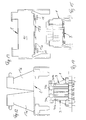
- Fig. 1 shows the cutting of a stamped sheet metal part 1, the has an approximately rectangular base plate region 10, which is limited by bending lines 11, 12, 13, 14. Along the bending line 11, an arm 15 is angled, the one has approximately triangular to trapezoidal outline and one Holding head 16 has. Tabs 17, 18 are on the holding head 16 molded. On the base plate 10 there are extensions 19, 20 provided that beyond the bending line 12 to form Feet 21, 22 are bent. More feet 23, 24 will be by bending longitudinal strips 25, 26 around the bending lines 13, 14 formed.
- Fig. 2 shows a flexprint plate 3, the one Kapton film 30 and a strip-shaped conductor print having a signal path 31 and grounding paths 32 and 33.
- the signal path 31 leads to an antenna contact area 34.
- the tracks 31, 32, 33 each have connection ends 35, 36, 37 with which they connect to corresponding connection areas 45, 46, 47 a circuit board 4 (Fig. 6) are attached.
- the flexprint plate has an approximately T-shaped Outline to accommodate two eyelets 38, 39 adjacent to the Contact field 34 are housed.
- the sheet metal blank 1 receives after bending around the Bending lines 11, 12, 13, 14 and cranking the tabs 17, 18 the form shown in FIGS. 3 to 5.
- This shape forms a frame to support the flexprint plate 3, as from 6 to 8 emerges.
- the feet 21, 22, 23, 24 through holes 41, 42, 43, 44 to the circuit board 4 inserted and anchored in it with conventional means and attached, for example by soldering.
- Fig. 6 shows an antenna 5 which in walls 6 a Housing is fixed and resilient to the abutment or abuts the antenna contact area 34.
- the rear one Antenna tip 51 can be at the level of the contact area 34 Take an angle of 90 ° ⁇ 10 °.
- the Support arm 15 bent at the transition to the head 16 to one Air gap 2 between the stamped sheet metal part 1 or its To create arm 15 and the flexprint plate 3.
- the Signal path 31 is in this way at a certain distance surrounded by metal parts 15, 32 and 33, whereby a Wave resistance of 50 ohms, for example, results as it is desired.
- the ends 35, 36, 37 of the Lanes 31, 32, 33 are with the connection panels 45, 46, 47 of the Circuit board 4 with their respective surfaces connected, which need not be explained in more detail.
- FIG. 9 to 11 show an application of the Antenna connector in the event that the antenna 5 as internal antenna when plugging in an external antenna 7 should be switched off.
- the head of the holding arm 15 points in In this case, a lateral extension 27 by a lateral extension 57 of the flexprint plate is covered on which is an antenna contact field 54, which with the Contact field 34 is connected via a bridge 55. If the external antenna 7 is inserted, it comes on the field 54 to support and bends the holding arm 15 resiliently so that the contact field 34 out of contact with the internal antenna 5 arrives, which is switched off.
- the associated flexprint plate 3 (FIGS. 14, 15) has two signal paths 31a, 31b, each with one Antenna contact field 34a or 34b and two grounding tracks 32a, 32b and 33a, 33b on the respective signal paths accompany.
- the support fields Wear nickel plating with gold layer.
- the areas 35, 36, 37 as well as 45, 46, 47 can be used for superficial reflow soldering to be prepared.
Landscapes
- Engineering & Computer Science (AREA)
- Computer Networks & Wireless Communication (AREA)
- Coupling Device And Connection With Printed Circuit (AREA)
Priority Applications (1)
| Application Number | Priority Date | Filing Date | Title |
|---|---|---|---|
| EP99111164A EP1061604A1 (fr) | 1999-06-08 | 1999-06-08 | Connecteur d'antenne |
Applications Claiming Priority (1)
| Application Number | Priority Date | Filing Date | Title |
|---|---|---|---|
| EP99111164A EP1061604A1 (fr) | 1999-06-08 | 1999-06-08 | Connecteur d'antenne |
Publications (1)
| Publication Number | Publication Date |
|---|---|
| EP1061604A1 true EP1061604A1 (fr) | 2000-12-20 |
Family
ID=8238321
Family Applications (1)
| Application Number | Title | Priority Date | Filing Date |
|---|---|---|---|
| EP99111164A Withdrawn EP1061604A1 (fr) | 1999-06-08 | 1999-06-08 | Connecteur d'antenne |
Country Status (1)
| Country | Link |
|---|---|
| EP (1) | EP1061604A1 (fr) |
Cited By (1)
| Publication number | Priority date | Publication date | Assignee | Title |
|---|---|---|---|---|
| CN110281709A (zh) * | 2019-06-12 | 2019-09-27 | 深圳市永奥图电子有限公司 | 一种外置式胎压监测器 |
Citations (5)
| Publication number | Priority date | Publication date | Assignee | Title |
|---|---|---|---|---|
| US4636016A (en) * | 1985-08-30 | 1987-01-13 | Motorola, Inc. | Accessory connector |
| EP0555949A1 (fr) * | 1992-02-14 | 1993-08-18 | Robert Karst GmbH & Co. KG. | Dispositif de fixation pour connecteur pour appareils des applications mobiles |
| EP0773633A2 (fr) * | 1995-11-08 | 1997-05-14 | Nokia Mobile Phones Ltd. | Boîtier de radio portable |
| US5835071A (en) * | 1996-09-25 | 1998-11-10 | Ericsson, Inc. | Shielded antenna connector |
| US5907817A (en) * | 1996-12-24 | 1999-05-25 | Ericsson Inc. | Radiotelephones with coplanar antenna connectors and related assembly methods |
-
1999
- 1999-06-08 EP EP99111164A patent/EP1061604A1/fr not_active Withdrawn
Patent Citations (5)
| Publication number | Priority date | Publication date | Assignee | Title |
|---|---|---|---|---|
| US4636016A (en) * | 1985-08-30 | 1987-01-13 | Motorola, Inc. | Accessory connector |
| EP0555949A1 (fr) * | 1992-02-14 | 1993-08-18 | Robert Karst GmbH & Co. KG. | Dispositif de fixation pour connecteur pour appareils des applications mobiles |
| EP0773633A2 (fr) * | 1995-11-08 | 1997-05-14 | Nokia Mobile Phones Ltd. | Boîtier de radio portable |
| US5835071A (en) * | 1996-09-25 | 1998-11-10 | Ericsson, Inc. | Shielded antenna connector |
| US5907817A (en) * | 1996-12-24 | 1999-05-25 | Ericsson Inc. | Radiotelephones with coplanar antenna connectors and related assembly methods |
Cited By (2)
| Publication number | Priority date | Publication date | Assignee | Title |
|---|---|---|---|---|
| CN110281709A (zh) * | 2019-06-12 | 2019-09-27 | 深圳市永奥图电子有限公司 | 一种外置式胎压监测器 |
| CN110281709B (zh) * | 2019-06-12 | 2024-01-16 | 深圳市永奥图电子有限公司 | 一种外置式胎压监测器 |
Similar Documents
| Publication | Publication Date | Title |
|---|---|---|
| DE69527817T2 (de) | Flachkabel, Verbindungsvorrichtung dafür und elektrisches Schaltungsapparat | |
| DE69112658T2 (de) | Abgeschirmter Verbinder. | |
| DE69634005T2 (de) | Steckverbinder mit integriertem leiterplattenzusammenbau | |
| DE69112500T2 (de) | Kontaktanordnung. | |
| EP2569827B1 (fr) | Système de bus avec rail de support | |
| DE4217205C2 (de) | Steckverbinder | |
| DE3535923C2 (fr) | ||
| DE112006002517T5 (de) | Chip-Widerstand | |
| DE69619033T2 (de) | Polaritätsempfindliche Schutzvorrichtung | |
| DE60310303T2 (de) | Leiterplattenrandverbinder und Karte | |
| DE69730174T2 (de) | Montagestruktur zur Befestigung eines elektrischen Modules auf einer Platte | |
| DE10153726A1 (de) | Flexible Schaltkreistafel und Verbindung der Struktur davon | |
| DE8008351U1 (de) | Mehradriger Verbinder | |
| DE3545527A1 (de) | Flexible elektrische verbindungsvorrichtung und verfahren zu ihrer herstellung | |
| EP0402739B1 (fr) | Dispositif pour coupler électriquement des unités électriques enfichables | |
| DE29808048U1 (de) | Verbindungsvorrichtung | |
| EP1061604A1 (fr) | Connecteur d'antenne | |
| EP1571735B1 (fr) | Composant électrotechnique | |
| WO1982003723A1 (fr) | Contact electrique, notamment pour circuits imprimes de petits appareils electriques | |
| DE60201537T2 (de) | Elektrische verbindungsanordnung für elektronische bauteile | |
| EP0144413A1 (fr) | Carte imprimee pour le montage en surface de circuits integres miniature et procede de fabrication de telles cartes imprimees | |
| DE8428437U1 (de) | Schaltungshybrid für elektronische Schaltungen | |
| DE69206977T2 (de) | Kontaktvorrichtung für ein elektrisches oder elektronisches bauteil | |
| DE2929612C2 (de) | Schaltungsanordnung in Microstrip-Bauweise für mit Leistungstransistoren bestückte Schaltungen der Höchstfrequenztechnik | |
| DE69701219T2 (de) | Elektronische baugruppe mit einer an einer spule verbundenen elektronischen einheit |
Legal Events
| Date | Code | Title | Description |
|---|---|---|---|
| PUAI | Public reference made under article 153(3) epc to a published international application that has entered the european phase |
Free format text: ORIGINAL CODE: 0009012 |
|
| AK | Designated contracting states |
Kind code of ref document: A1 Designated state(s): DE FR GB IT |
|
| AX | Request for extension of the european patent |
Free format text: AL;LT;LV;MK;RO;SI |
|
| 17P | Request for examination filed |
Effective date: 20010612 |
|
| AKX | Designation fees paid |
Free format text: DE FR GB IT |
|
| STAA | Information on the status of an ep patent application or granted ep patent |
Free format text: STATUS: THE APPLICATION IS DEEMED TO BE WITHDRAWN |
|
| 18D | Application deemed to be withdrawn |
Effective date: 20021231 |