EP1061783A2 - Keramik-Metall-Substrat, insbesondere Mehrfachsubstrat - Google Patents
Keramik-Metall-Substrat, insbesondere Mehrfachsubstrat Download PDFInfo
- Publication number
- EP1061783A2 EP1061783A2 EP00112228A EP00112228A EP1061783A2 EP 1061783 A2 EP1061783 A2 EP 1061783A2 EP 00112228 A EP00112228 A EP 00112228A EP 00112228 A EP00112228 A EP 00112228A EP 1061783 A2 EP1061783 A2 EP 1061783A2
- Authority
- EP
- European Patent Office
- Prior art keywords
- metal
- ceramic
- edge
- predetermined breaking
- substrate
- Prior art date
- Legal status (The legal status is an assumption and is not a legal conclusion. Google has not performed a legal analysis and makes no representation as to the accuracy of the status listed.)
- Granted
Links
Images



Classifications
-
- H—ELECTRICITY
- H10—SEMICONDUCTOR DEVICES; ELECTRIC SOLID-STATE DEVICES NOT OTHERWISE PROVIDED FOR
- H10W—GENERIC PACKAGES, INTERCONNECTIONS, CONNECTORS OR OTHER CONSTRUCTIONAL DETAILS OF DEVICES COVERED BY CLASS H10
- H10W99/00—Subject matter not provided for in other groups of this subclass
-
- B—PERFORMING OPERATIONS; TRANSPORTING
- B23—MACHINE TOOLS; METAL-WORKING NOT OTHERWISE PROVIDED FOR
- B23K—SOLDERING OR UNSOLDERING; WELDING; CLADDING OR PLATING BY SOLDERING OR WELDING; CUTTING BY APPLYING HEAT LOCALLY, e.g. FLAME CUTTING; WORKING BY LASER BEAM
- B23K26/00—Working by laser beam, e.g. welding, cutting or boring
- B23K26/0006—Working by laser beam, e.g. welding, cutting or boring taking account of the properties of the material involved
-
- B—PERFORMING OPERATIONS; TRANSPORTING
- B23—MACHINE TOOLS; METAL-WORKING NOT OTHERWISE PROVIDED FOR
- B23K—SOLDERING OR UNSOLDERING; WELDING; CLADDING OR PLATING BY SOLDERING OR WELDING; CUTTING BY APPLYING HEAT LOCALLY, e.g. FLAME CUTTING; WORKING BY LASER BEAM
- B23K26/00—Working by laser beam, e.g. welding, cutting or boring
- B23K26/352—Working by laser beam, e.g. welding, cutting or boring for surface treatment
- B23K26/359—Working by laser beam, e.g. welding, cutting or boring for surface treatment by providing a line or line pattern, e.g. a dotted break initiation line
-
- B—PERFORMING OPERATIONS; TRANSPORTING
- B23—MACHINE TOOLS; METAL-WORKING NOT OTHERWISE PROVIDED FOR
- B23K—SOLDERING OR UNSOLDERING; WELDING; CLADDING OR PLATING BY SOLDERING OR WELDING; CUTTING BY APPLYING HEAT LOCALLY, e.g. FLAME CUTTING; WORKING BY LASER BEAM
- B23K26/00—Working by laser beam, e.g. welding, cutting or boring
- B23K26/36—Removing material
- B23K26/361—Removing material for deburring or mechanical trimming
-
- B—PERFORMING OPERATIONS; TRANSPORTING
- B23—MACHINE TOOLS; METAL-WORKING NOT OTHERWISE PROVIDED FOR
- B23K—SOLDERING OR UNSOLDERING; WELDING; CLADDING OR PLATING BY SOLDERING OR WELDING; CUTTING BY APPLYING HEAT LOCALLY, e.g. FLAME CUTTING; WORKING BY LASER BEAM
- B23K26/00—Working by laser beam, e.g. welding, cutting or boring
- B23K26/36—Removing material
- B23K26/40—Removing material taking account of the properties of the material involved
-
- C—CHEMISTRY; METALLURGY
- C04—CEMENTS; CONCRETE; ARTIFICIAL STONE; CERAMICS; REFRACTORIES
- C04B—LIME, MAGNESIA; SLAG; CEMENTS; COMPOSITIONS THEREOF, e.g. MORTARS, CONCRETE OR LIKE BUILDING MATERIALS; ARTIFICIAL STONE; CERAMICS; REFRACTORIES; TREATMENT OF NATURAL STONE
- C04B37/00—Joining burned ceramic articles with other burned ceramic articles or other articles by heating
- C04B37/02—Joining burned ceramic articles with other burned ceramic articles or other articles by heating with metallic articles
- C04B37/021—Joining burned ceramic articles with other burned ceramic articles or other articles by heating with metallic articles in a direct manner, e.g. direct copper bonding [DCB]
-
- H—ELECTRICITY
- H05—ELECTRIC TECHNIQUES NOT OTHERWISE PROVIDED FOR
- H05K—PRINTED CIRCUITS; CASINGS OR CONSTRUCTIONAL DETAILS OF ELECTRIC APPARATUS; MANUFACTURE OF ASSEMBLAGES OF ELECTRICAL COMPONENTS
- H05K1/00—Printed circuits
- H05K1/02—Details
- H05K1/0271—Arrangements for reducing stress or warp in rigid printed circuit boards, e.g. caused by loads, vibrations or differences in thermal expansion
-
- H—ELECTRICITY
- H10—SEMICONDUCTOR DEVICES; ELECTRIC SOLID-STATE DEVICES NOT OTHERWISE PROVIDED FOR
- H10W—GENERIC PACKAGES, INTERCONNECTIONS, CONNECTORS OR OTHER CONSTRUCTIONAL DETAILS OF DEVICES COVERED BY CLASS H10
- H10W40/00—Arrangements for thermal protection or thermal control
- H10W40/20—Arrangements for cooling
- H10W40/25—Arrangements for cooling characterised by their materials
- H10W40/255—Arrangements for cooling characterised by their materials having a laminate or multilayered structure, e.g. direct bond copper [DBC] ceramic substrates
-
- H—ELECTRICITY
- H10—SEMICONDUCTOR DEVICES; ELECTRIC SOLID-STATE DEVICES NOT OTHERWISE PROVIDED FOR
- H10W—GENERIC PACKAGES, INTERCONNECTIONS, CONNECTORS OR OTHER CONSTRUCTIONAL DETAILS OF DEVICES COVERED BY CLASS H10
- H10W70/00—Package substrates; Interposers; Redistribution layers [RDL]
- H10W70/60—Insulating or insulated package substrates; Interposers; Redistribution layers
- H10W70/62—Insulating or insulated package substrates; Interposers; Redistribution layers characterised by their interconnections
- H10W70/65—Shapes or dispositions of interconnections
-
- H—ELECTRICITY
- H10—SEMICONDUCTOR DEVICES; ELECTRIC SOLID-STATE DEVICES NOT OTHERWISE PROVIDED FOR
- H10W—GENERIC PACKAGES, INTERCONNECTIONS, CONNECTORS OR OTHER CONSTRUCTIONAL DETAILS OF DEVICES COVERED BY CLASS H10
- H10W72/00—Interconnections or connectors in packages
- H10W72/01—Manufacture or treatment
- H10W72/0198—Manufacture or treatment batch processes
-
- B—PERFORMING OPERATIONS; TRANSPORTING
- B23—MACHINE TOOLS; METAL-WORKING NOT OTHERWISE PROVIDED FOR
- B23K—SOLDERING OR UNSOLDERING; WELDING; CLADDING OR PLATING BY SOLDERING OR WELDING; CUTTING BY APPLYING HEAT LOCALLY, e.g. FLAME CUTTING; WORKING BY LASER BEAM
- B23K2103/00—Materials to be soldered, welded or cut
- B23K2103/16—Composite materials
-
- B—PERFORMING OPERATIONS; TRANSPORTING
- B23—MACHINE TOOLS; METAL-WORKING NOT OTHERWISE PROVIDED FOR
- B23K—SOLDERING OR UNSOLDERING; WELDING; CLADDING OR PLATING BY SOLDERING OR WELDING; CUTTING BY APPLYING HEAT LOCALLY, e.g. FLAME CUTTING; WORKING BY LASER BEAM
- B23K2103/00—Materials to be soldered, welded or cut
- B23K2103/16—Composite materials
- B23K2103/166—Multilayered materials
- B23K2103/172—Multilayered materials wherein at least one of the layers is non-metallic
-
- B—PERFORMING OPERATIONS; TRANSPORTING
- B23—MACHINE TOOLS; METAL-WORKING NOT OTHERWISE PROVIDED FOR
- B23K—SOLDERING OR UNSOLDERING; WELDING; CLADDING OR PLATING BY SOLDERING OR WELDING; CUTTING BY APPLYING HEAT LOCALLY, e.g. FLAME CUTTING; WORKING BY LASER BEAM
- B23K2103/00—Materials to be soldered, welded or cut
- B23K2103/50—Inorganic materials other than metals or composite materials
-
- B—PERFORMING OPERATIONS; TRANSPORTING
- B23—MACHINE TOOLS; METAL-WORKING NOT OTHERWISE PROVIDED FOR
- B23K—SOLDERING OR UNSOLDERING; WELDING; CLADDING OR PLATING BY SOLDERING OR WELDING; CUTTING BY APPLYING HEAT LOCALLY, e.g. FLAME CUTTING; WORKING BY LASER BEAM
- B23K2103/00—Materials to be soldered, welded or cut
- B23K2103/50—Inorganic materials other than metals or composite materials
- B23K2103/52—Ceramics
-
- C—CHEMISTRY; METALLURGY
- C04—CEMENTS; CONCRETE; ARTIFICIAL STONE; CERAMICS; REFRACTORIES
- C04B—LIME, MAGNESIA; SLAG; CEMENTS; COMPOSITIONS THEREOF, e.g. MORTARS, CONCRETE OR LIKE BUILDING MATERIALS; ARTIFICIAL STONE; CERAMICS; REFRACTORIES; TREATMENT OF NATURAL STONE
- C04B2237/00—Aspects relating to ceramic laminates or to joining of ceramic articles with other articles by heating
- C04B2237/30—Composition of layers of ceramic laminates or of ceramic or metallic articles to be joined by heating, e.g. Si substrates
- C04B2237/32—Ceramic
- C04B2237/34—Oxidic
- C04B2237/343—Alumina or aluminates
-
- C—CHEMISTRY; METALLURGY
- C04—CEMENTS; CONCRETE; ARTIFICIAL STONE; CERAMICS; REFRACTORIES
- C04B—LIME, MAGNESIA; SLAG; CEMENTS; COMPOSITIONS THEREOF, e.g. MORTARS, CONCRETE OR LIKE BUILDING MATERIALS; ARTIFICIAL STONE; CERAMICS; REFRACTORIES; TREATMENT OF NATURAL STONE
- C04B2237/00—Aspects relating to ceramic laminates or to joining of ceramic articles with other articles by heating
- C04B2237/30—Composition of layers of ceramic laminates or of ceramic or metallic articles to be joined by heating, e.g. Si substrates
- C04B2237/32—Ceramic
- C04B2237/36—Non-oxidic
- C04B2237/366—Aluminium nitride
-
- C—CHEMISTRY; METALLURGY
- C04—CEMENTS; CONCRETE; ARTIFICIAL STONE; CERAMICS; REFRACTORIES
- C04B—LIME, MAGNESIA; SLAG; CEMENTS; COMPOSITIONS THEREOF, e.g. MORTARS, CONCRETE OR LIKE BUILDING MATERIALS; ARTIFICIAL STONE; CERAMICS; REFRACTORIES; TREATMENT OF NATURAL STONE
- C04B2237/00—Aspects relating to ceramic laminates or to joining of ceramic articles with other articles by heating
- C04B2237/30—Composition of layers of ceramic laminates or of ceramic or metallic articles to be joined by heating, e.g. Si substrates
- C04B2237/40—Metallic
-
- C—CHEMISTRY; METALLURGY
- C04—CEMENTS; CONCRETE; ARTIFICIAL STONE; CERAMICS; REFRACTORIES
- C04B—LIME, MAGNESIA; SLAG; CEMENTS; COMPOSITIONS THEREOF, e.g. MORTARS, CONCRETE OR LIKE BUILDING MATERIALS; ARTIFICIAL STONE; CERAMICS; REFRACTORIES; TREATMENT OF NATURAL STONE
- C04B2237/00—Aspects relating to ceramic laminates or to joining of ceramic articles with other articles by heating
- C04B2237/50—Processing aspects relating to ceramic laminates or to the joining of ceramic articles with other articles by heating
- C04B2237/86—Joining of two substrates at their largest surfaces, one surface being complete joined and covered, the other surface not, e.g. a small plate joined at it's largest surface on top of a larger plate
-
- H—ELECTRICITY
- H05—ELECTRIC TECHNIQUES NOT OTHERWISE PROVIDED FOR
- H05K—PRINTED CIRCUITS; CASINGS OR CONSTRUCTIONAL DETAILS OF ELECTRIC APPARATUS; MANUFACTURE OF ASSEMBLAGES OF ELECTRICAL COMPONENTS
- H05K1/00—Printed circuits
- H05K1/02—Details
- H05K1/03—Use of materials for the substrate
- H05K1/0306—Inorganic insulating substrates, e.g. ceramic, glass
-
- H—ELECTRICITY
- H05—ELECTRIC TECHNIQUES NOT OTHERWISE PROVIDED FOR
- H05K—PRINTED CIRCUITS; CASINGS OR CONSTRUCTIONAL DETAILS OF ELECTRIC APPARATUS; MANUFACTURE OF ASSEMBLAGES OF ELECTRICAL COMPONENTS
- H05K2201/00—Indexing scheme relating to printed circuits covered by H05K1/00
- H05K2201/03—Conductive materials
- H05K2201/0332—Structure of the conductor
- H05K2201/0335—Layered conductors or foils
- H05K2201/0355—Metal foils
-
- H—ELECTRICITY
- H05—ELECTRIC TECHNIQUES NOT OTHERWISE PROVIDED FOR
- H05K—PRINTED CIRCUITS; CASINGS OR CONSTRUCTIONAL DETAILS OF ELECTRIC APPARATUS; MANUFACTURE OF ASSEMBLAGES OF ELECTRICAL COMPONENTS
- H05K2201/00—Indexing scheme relating to printed circuits covered by H05K1/00
- H05K2201/09—Shape and layout
- H05K2201/09009—Substrate related
- H05K2201/09036—Recesses or grooves in insulating substrate
-
- H—ELECTRICITY
- H05—ELECTRIC TECHNIQUES NOT OTHERWISE PROVIDED FOR
- H05K—PRINTED CIRCUITS; CASINGS OR CONSTRUCTIONAL DETAILS OF ELECTRIC APPARATUS; MANUFACTURE OF ASSEMBLAGES OF ELECTRICAL COMPONENTS
- H05K2201/00—Indexing scheme relating to printed circuits covered by H05K1/00
- H05K2201/09—Shape and layout
- H05K2201/09009—Substrate related
- H05K2201/0909—Preformed cutting or breaking line
-
- H—ELECTRICITY
- H05—ELECTRIC TECHNIQUES NOT OTHERWISE PROVIDED FOR
- H05K—PRINTED CIRCUITS; CASINGS OR CONSTRUCTIONAL DETAILS OF ELECTRIC APPARATUS; MANUFACTURE OF ASSEMBLAGES OF ELECTRICAL COMPONENTS
- H05K2201/00—Indexing scheme relating to printed circuits covered by H05K1/00
- H05K2201/09—Shape and layout
- H05K2201/09209—Shape and layout details of conductors
- H05K2201/09654—Shape and layout details of conductors covering at least two types of conductors provided for in H05K2201/09218 - H05K2201/095
- H05K2201/0969—Apertured conductors
-
- H—ELECTRICITY
- H05—ELECTRIC TECHNIQUES NOT OTHERWISE PROVIDED FOR
- H05K—PRINTED CIRCUITS; CASINGS OR CONSTRUCTIONAL DETAILS OF ELECTRIC APPARATUS; MANUFACTURE OF ASSEMBLAGES OF ELECTRICAL COMPONENTS
- H05K2201/00—Indexing scheme relating to printed circuits covered by H05K1/00
- H05K2201/09—Shape and layout
- H05K2201/09209—Shape and layout details of conductors
- H05K2201/09654—Shape and layout details of conductors covering at least two types of conductors provided for in H05K2201/09218 - H05K2201/095
- H05K2201/09745—Recess in conductor, e.g. in pad or in metallic substrate
-
- H—ELECTRICITY
- H05—ELECTRIC TECHNIQUES NOT OTHERWISE PROVIDED FOR
- H05K—PRINTED CIRCUITS; CASINGS OR CONSTRUCTIONAL DETAILS OF ELECTRIC APPARATUS; MANUFACTURE OF ASSEMBLAGES OF ELECTRICAL COMPONENTS
- H05K2201/00—Indexing scheme relating to printed circuits covered by H05K1/00
- H05K2201/09—Shape and layout
- H05K2201/09818—Shape or layout details not covered by a single group of H05K2201/09009 - H05K2201/09809
- H05K2201/09845—Stepped hole, via, edge, bump or conductor
-
- H—ELECTRICITY
- H05—ELECTRIC TECHNIQUES NOT OTHERWISE PROVIDED FOR
- H05K—PRINTED CIRCUITS; CASINGS OR CONSTRUCTIONAL DETAILS OF ELECTRIC APPARATUS; MANUFACTURE OF ASSEMBLAGES OF ELECTRICAL COMPONENTS
- H05K2203/00—Indexing scheme relating to apparatus or processes for manufacturing printed circuits covered by H05K3/00
- H05K2203/30—Details of processes not otherwise provided for in H05K2203/01 - H05K2203/17
- H05K2203/302—Bending a rigid substrate; Breaking rigid substrates by bending
-
- H—ELECTRICITY
- H05—ELECTRIC TECHNIQUES NOT OTHERWISE PROVIDED FOR
- H05K—PRINTED CIRCUITS; CASINGS OR CONSTRUCTIONAL DETAILS OF ELECTRIC APPARATUS; MANUFACTURE OF ASSEMBLAGES OF ELECTRICAL COMPONENTS
- H05K3/00—Apparatus or processes for manufacturing printed circuits
- H05K3/0011—Working of insulating substrates or insulating layers
- H05K3/0044—Mechanical working of the substrate, e.g. drilling or punching
- H05K3/0052—Depaneling, i.e. dividing a panel into circuit boards; Working of the edges of circuit boards
-
- H—ELECTRICITY
- H10—SEMICONDUCTOR DEVICES; ELECTRIC SOLID-STATE DEVICES NOT OTHERWISE PROVIDED FOR
- H10W—GENERIC PACKAGES, INTERCONNECTIONS, CONNECTORS OR OTHER CONSTRUCTIONAL DETAILS OF DEVICES COVERED BY CLASS H10
- H10W72/00—Interconnections or connectors in packages
- H10W72/50—Bond wires
- H10W72/541—Dispositions of bond wires
- H10W72/5445—Dispositions of bond wires being orthogonal to a side surface of the chip, e.g. parallel arrangements
-
- H—ELECTRICITY
- H10—SEMICONDUCTOR DEVICES; ELECTRIC SOLID-STATE DEVICES NOT OTHERWISE PROVIDED FOR
- H10W—GENERIC PACKAGES, INTERCONNECTIONS, CONNECTORS OR OTHER CONSTRUCTIONAL DETAILS OF DEVICES COVERED BY CLASS H10
- H10W72/00—Interconnections or connectors in packages
- H10W72/50—Bond wires
- H10W72/541—Dispositions of bond wires
- H10W72/547—Dispositions of multiple bond wires
- H10W72/5473—Dispositions of multiple bond wires multiple bond wires connected to a common bond pad
-
- H—ELECTRICITY
- H10—SEMICONDUCTOR DEVICES; ELECTRIC SOLID-STATE DEVICES NOT OTHERWISE PROVIDED FOR
- H10W—GENERIC PACKAGES, INTERCONNECTIONS, CONNECTORS OR OTHER CONSTRUCTIONAL DETAILS OF DEVICES COVERED BY CLASS H10
- H10W90/00—Package configurations
- H10W90/701—Package configurations characterised by the relative positions of pads or connectors relative to package parts
- H10W90/751—Package configurations characterised by the relative positions of pads or connectors relative to package parts of bond wires
- H10W90/754—Package configurations characterised by the relative positions of pads or connectors relative to package parts of bond wires between a chip and a stacked insulating package substrate, interposer or RDL
-
- Y—GENERAL TAGGING OF NEW TECHNOLOGICAL DEVELOPMENTS; GENERAL TAGGING OF CROSS-SECTIONAL TECHNOLOGIES SPANNING OVER SEVERAL SECTIONS OF THE IPC; TECHNICAL SUBJECTS COVERED BY FORMER USPC CROSS-REFERENCE ART COLLECTIONS [XRACs] AND DIGESTS
- Y10—TECHNICAL SUBJECTS COVERED BY FORMER USPC
- Y10T—TECHNICAL SUBJECTS COVERED BY FORMER US CLASSIFICATION
- Y10T428/00—Stock material or miscellaneous articles
- Y10T428/15—Sheet, web, or layer weakened to permit separation through thickness
-
- Y—GENERAL TAGGING OF NEW TECHNOLOGICAL DEVELOPMENTS; GENERAL TAGGING OF CROSS-SECTIONAL TECHNOLOGIES SPANNING OVER SEVERAL SECTIONS OF THE IPC; TECHNICAL SUBJECTS COVERED BY FORMER USPC CROSS-REFERENCE ART COLLECTIONS [XRACs] AND DIGESTS
- Y10—TECHNICAL SUBJECTS COVERED BY FORMER USPC
- Y10T—TECHNICAL SUBJECTS COVERED BY FORMER US CLASSIFICATION
- Y10T428/00—Stock material or miscellaneous articles
- Y10T428/24—Structurally defined web or sheet [e.g., overall dimension, etc.]
- Y10T428/24479—Structurally defined web or sheet [e.g., overall dimension, etc.] including variation in thickness
Definitions
- the invention relates to a ceramic-metal substrate according to the preamble Claim 1.
- Ceramic-metal substrates and in particular ceramic-copper substrates are known. These substrates are used to manufacture electrical circuits, in particular power circuits, and form the ones there PCB ".
- such substrates have a ceramic layer on both Surface sides are each provided with a metallization, of which e.g. the Metallization on the top of the ceramic layer using, for example an etching technique is structured such that this metallization is then used for the Circuit forms necessary traces, contact areas, etc.
- a metallization of which e.g. the Metallization on the top of the ceramic layer using, for example an etching technique is structured such that this metallization is then used for the Circuit forms necessary traces, contact areas, etc.
- the metallizations are applied in hot processes, ie in processes in which not insignificant temperatures are used.
- a ceramic for example on an aluminum oxide ceramic
- DCB process Direct-Copper-Bond-Technology
- metal or copper foils or metal or copper sheets forming the metallization which have a layer or a coating (melting layer) of a chemical on their surface sides
- this layer or this coating forms a eutectic with a melting temperature below the melting temperature of the metal (for example copper), so that it can be connected to one another by placing the film on the ceramic and by heating all the layers, specifically by melting the metal or copper only in the area of the melting layer or oxide layer.
- the metal for example copper
- the object of the invention is to avoid this disadvantage.
- the inventive design surprisingly wild or uncontrolled breaks when cutting the ceramic-metal substrate is essential reduced (proven dimensions up to 75%).
- FIGS. 1-13 three are each vertical in FIGS. 1-13 mutually arranged spatial axes (X axis, Y axis and Z axis) specified by where the X and Y axes define the level of the respective multiple substrate (X-Y level) and the Z axis in the thickness direction of the respective multiple substrate lies.
- the multiple substrate shown in FIGS. 1-4 and generally designated 1 (also large card) consists essentially of a ceramic plate or Ceramic layer 2, for example an aluminum nitride ceramic or Alumina ceramic and in the embodiment of Figures 1-3 on both Surface sides is provided with a structured metallization, on the Top with metallization 3 and underside with metallization 4.
- a metal foil for example a Copper foil is connected flat to the ceramic layer 2.
- the structuring of the Metallization 3 and 4 is with the usual means known to those skilled in the art performed, for example using masking and etching techniques.
- the metallization 3 is structured on the upper side in such a way that that this forms several metal surfaces 3 ', which in several, each in the direction of the X axis and adjoining one another in the direction of the Y axis Rows are provided.
- the multiple substrate 1 is in the embodiment shown with a rectangular circumferential line, in such a way that the shorter Peripheral sides in the direction of the X axis and the longer peripheral axes in Extend in the direction of the Y axis.
- the metallization 3 is further structured so that it runs along the edges 5 and 6 each a rectangular or strip-shaped metal surface 3 '' (along the edges 5) and 3 '' '(along the edges 6), the two metal surfaces 3' ' each essentially over the entire width (distance between the two edges 6) of the Multiple substrates 1 extend and the two metal surfaces 3 ′′ at both ends each end near a metal surface (3 '').
- edges of the metal surface 3 ' lie parallel to the edges 5 and 6 and thus also in the X-axis or Y-axis.
- the strip-shaped or elongated rectangular metal surfaces 3 '' and 3 '' ' with their edges parallel to the edges 5 and 6 and thus in the direction of the X axis and Y axis.
- All metal surfaces 3 ', 3' ', 3' '' are each from an adjacent metal surface spaced, as will be discussed in more detail below.
- these predetermined breaking lines 7 and 8 incisions are introduced, in such a way that these predetermined breaking lines are not only between the individual, the individual substrates forming metal surfaces 3 ', but also between the metal surfaces 3' ' and adjacent metal surfaces 3 'and 3' '' and between the metal surfaces 3 '' ' and adjacent metal surfaces 3 '.
- the predetermined breaking line 7 extends in detail in the direction of the X axis and the predetermined breaking lines 8 in the direction of the Y axis, wherein in each case an outside predetermined breaking line 7, which is adjacent to the metal surface 3 ′′, in the illustrated embodiment over the entire width of the Multiple substrates 1 extends, i.e. also in the exposed areas of the top the ceramic layer 2 between the metallizations 3 ′′ and 3 ′′ ′′.
- the two outside lying predetermined breaking lines 8 each extend between the respective Metal surface 3 '' 'and the adjacent metal surfaces 3' and end at illustrated embodiment in each case on the metal surfaces 3 ′′ or on the parallel to outer predetermined breaking lines 7 running these metal surfaces.
- the metallization 4 on the underside of the multiple substrate 1 is structured such that this metallization forms a multiplicity of metal surfaces 4 'which correspond to the metal surfaces 3' correspond and each of which has a metal surface 4 'of a metal surface 3' directly opposite.
- the metal surfaces 4 ' are in the same way as that Metal surfaces 3 'are provided in several rows and are parallel with their edges to the edges 5 and 6.
- the metallization 4 forms metal surfaces 4 ′′ and 4 '' ', which correspond to the metal surfaces 3' 'or 3' '' and each of which metal surface 4 ′′ of a metal surface 3 ′′ and each metal surface 4 ′′ ′′ of a metal surface 3 ′′ ′′ lies.
- the metal surfaces 4 ', 4' 'and 4' '' are at the predetermined breaking lines 7 and 8 spaced from each other so that the underside of the ceramic layer 2 is exposed there.
- the multiple substrate can in particular according to the Structuring the metal surfaces 3 'and after the placement in individual substrates or in electrical components formed by these individual substrates by breaking along the Break lines 7 and 8 are separated, for this purpose first opening the Multiple substrates 1 is necessary in that the metal surfaces 3 '' and 3 '' ' and 4 '' and 4 ''' 'edges are broken off, along the outer predetermined breaking lines 7 and 8.
- This opening is only in a certain Sequences possible, namely in that the metal surfaces 3 ′′ and 4 '' outer edges and then the metal surfaces 3 '' 'and 4' '' having outer edges can be broken off.
- FIG. 3 shows a partial section through the multiple substrate of FIG. 1.
- the planes perpendicular to the XY plane denote the Include predetermined breaking lines 7 and 8.
- have all metal surfaces 4 'from these center planes SE each have a distance d1.
- the Edges of all metal surfaces 3 ', 3' 'and 3' '' have a parallel to that each edge, adjacent plane SE a distance of d2. This applies both for those parallel to the XZ plane and for those parallel to the YZ plane arranged levels SE.
- the thickness of the metallization is 3 and 4 for example 0.15-1.0 mm.
- the respective distance d2 is greater than or equal to d1, e.g. d1 in the order of magnitude from 1.0 to 0.05 mm. In the case of the multiple substrate 1, the distances d2 are larger than 1 mm.
- the predetermined breaking lines 7 and 8 are, for example, by laser treatment, generated for example by laser scribing.
- the predetermined breaking lines 7 and 8 can also be produced in other ways, for example by mechanical processing.
- This edge weakening 10 can, as will be explained in more detail below, in be realized in different ways, but is in any case designed so that in Area of this edge weakening 10, the metal volume or the amount of metal each Volume unit is reduced.
- the width of the edge weakening is shown in FIG a denotes and is for example in the order of magnitude between 0.2 and 6 mm.
- the reduction in the amount of metal or the volume of metal is such that at the Edge weakening 10 the amount of metal only about 10 to 80% of the amount of metal one Is metal surface 4 'without edge weakening, in each case based on one certain volume unit.
- the edge weakening 10 is also on the Metal surfaces 4 '' and 4 '' 'are provided, specifically along the predetermined breaking lines 7 and 8 adjacent edges, i.e. along the levels SE.
- this edge weakening 10 makes it possible for the To provide metal surfaces 4 'with only a small distance d1 from the planes SE and nevertheless greatly reduce uncontrolled breaks 9, so that a total Reduction of scrap compared to conventional multiple substrates 75% is detectable.
- Edge weakening on the metal surfaces 3 ', 3' 'and 3' '' is then necessary or at least makes sense if the distances d2 are less than 1 mm.
- FIGS. 6-15 show various options for the training as examples the edge weakening 10.
- an edge weakening 10a shown, which is formed by the fact that the adjacent edges of the planes SE Metal surfaces 4 ', 4' ', 4' '' are beveled, the bevel formed here Edge surface 11, for example at an angle ⁇ , which is less than 45 °.
- FIGS. 6 and 7 show an edge weakening 10b, which is formed by that along the edges of the metal surfaces 4 ', 4' ', 4' '' adjacent to the planes SE Rows of hole-like depressions 12 are formed, these depressions 12 to reach the underside of the ceramic layer 2 and for example a diameter have from about 0.4 to 0.5 mm.
- the recesses 12 form in this Embodiment a simple row of holes.
- the depressions 12 have a diameter of approximately 0.5 mm.
- the width a of the Edge weakening 10b, within the (width) also the depressions 12 is, for example, 0.8 mm, namely at a distance d1 of about 0.5 mm.
- the width a is defined so that a is the maximum distance that the Have edges of the depressions 12 from the adjacent edge of the metallization.
- FIG. 8 shows a possible embodiment in which the edge weakening 10c from the outside, i.e. the edges of the respective metallization 4 ', 4' ', 4' '' immediately adjacent recesses 12 and further recesses inside 13 is formed.
- the latter are each offset from the recesses 12 and form an inner one in addition to the outer row of holes (depressions 12) Row of holes (wells 13), both the wells 12 and the wells 13 reach to the bottom of the ceramic layer 2.
- the diameter of the In this embodiment, depressions 13 are smaller than the diameter of the Indentations 12.
- the width a of the edge weakening is 10c, all depressions 12 and 13 are located within (width a), approximately 1.4 mm, with the diameter of the outer recesses approximately 0.6 mm and the inner Depressions is about 0.4 mm.
- the width a is defined so that a is the maximum distance is the edges of the recesses 13 from the neighboring one Have edge of the metallization.
- FIG. 9 shows, as a further possibility, an edge weakening 10d, which thereby is formed that the edges or edges of the planes SE
- Metal surfaces 4 ', 4' 'and 4' '' with depressions 14 open towards these edges are provided so that there are meandering edges.
- the wells 14 in turn extend to the underside of the ceramic layer 2.
- edge weakening 10b - 10d Possibility of all or only some of the wells 12, 13 and 14 see above to ensure that they do not reach the bottom of the ceramic layer 2, but still a rest of the Metallization 4 remains.
- FIGS. 10 and 11 show, as a further possibility, an edge weakening 10e, which by a gradation 15 of the edges adjacent to the levels SE Metal surfaces 4 ', 4' ', 4' '' is formed, i.e. within the width a of Edge weakening 10e increases the thickness of the material of the respective metal surface step-wise, in the execution of Figures 9 and 10 in one step.
- an edge weakening 10e which by a gradation 15 of the edges adjacent to the levels SE Metal surfaces 4 ', 4' ', 4' '' is formed, i.e. within the width a of Edge weakening 10e increases the thickness of the material of the respective metal surface step-wise, in the execution of Figures 9 and 10 in one step.
- several stages 15 can also be provided.
- FIGS. 11 and 12 show a further possible embodiment Edge weakening 10f, which is formed in that the metal surfaces 4 ', 4' 'and 4 '' 'are each provided with a groove-like recess 16 which extends along the the edges of the planes SE and adjacent to these planes Metal surfaces extends, the recess 16 on the metal surfaces 4 'as in itself closed groove is executed.
- FIGS. 10-13 Edge weakening 10e and 10f also for the metal surfaces 3 ', 3' 'and 3' '' shown.
- edge weakenings 10a-10f also combine can be on either side of the multiple substrate 1 or on multiple pages. Furthermore, it is understood that edge weakening 10th are of course only provided where corresponding metal surfaces 3 ', 3 '', 3 '' 'or 4', 4 '', 4 '' 'are provided.
- Figures 14 and 15 show in representations similar to Figures 1 and 3 as Another possible embodiment of a multiple substrate 1a, which differs from that Multiple substrate 1 essentially differs only in that the to Edges 5 and 6 provided metal surfaces 4 '' and 4 '' 'are not present but only the metal surfaces 3 '' and 3 '' 'on the top of the Multiple substrates.
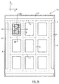
- FIG. 16 shows a multiple substrate 1b which, for example, Corresponds to multiple substrate 1 or 1a, but with the one on the top provided metal surfaces 3 'to form conductor tracks, contact surfaces, etc. for the Individual substrates are structured, as is shown in this figure with the numbers 17, 18 and 19 is indicated schematically.
- the structured surface areas 18 Components applied in the form of semiconductor chips 20, which with the associated, structured contact areas or connections forming structured areas 17 and 18 are electrically connected by wire bonds.
- all metal surfaces 3' are in this way structured and equipped with components, so that thereby a large card or Multiple conductor plate or an assembled multiple substrate is obtained, which only after assembly in the individual substrates or in the individual of these formed assemblies or circuits is separated.
- Edge weakening 10 on the metal surfaces 4 ', 4' 'or 4' '' (of course only insofar as these metal surfaces are present) and possibly also on the metal surfaces 3 ', 3' ' and 3 '' 'along all edges or edges adjacent to a plane SE intended.
- FIG. 17 shows a representation similar to FIG. 2 as a further possibility Multiple substrate 1c, in which edge or edge weakening 10 only along one Part of the edges of the metal surfaces 4 ', 4' 'or 4' '' and possibly also only on part the edges of the metal surfaces 3 ', 3' 'and 3' '' are provided, again of course, only if the metal surface in question actually exists.
- the embodiment shown in FIG. 17 is based on the knowledge that wild breaks 9 preferably occur when separating or breaking the Multiple substrates in individual substrates during the respective breaking process along one Break line 7 or 8 is broken, which extends over several individual substrates extends.
- the multiple substrate 1c is separated after rule or breaking sequence given below, may be on those edges of the metal surfaces 3 'which run between these metal surfaces 3' Break lines 8 or the levels SE are adjacent, which between the Include metal surfaces 4 'running predetermined breaking line 8, on a Edge weakening 10 can be dispensed with.
- edges of the metal surfaces 4 ', 4' ', 4' '' are the (edges) with an edge weakening 10 are provided, additionally hatched.
- the edges, the do not have an edge weakening 10 are shown as a straight line.
- Break lines 8 are carried out, the length of which is only the width of a single substrate corresponds, wild breaks 9 are unlikely to break, so that along the predetermined breaking lines 8 running between the metal surfaces 3 'or 4' an edge weakening 10 can be dispensed with.
- edge weakenings are then 10 in any case also along the predetermined breaking lines 8 running between the individual substrates required while on edge weakening along the between the Break lines 7 running individual substrates can be dispensed with.
- breaking should always be as short as possible
- Predetermined breaking lines should take place, i.e. with a rectangular configuration of the Multiple substrates with the longer length in the direction of the Y axis and the shorter one
- the width in the X-axis is expediently broken into the strips along the shorter breaking lines 8.
Landscapes
- Engineering & Computer Science (AREA)
- Physics & Mathematics (AREA)
- Optics & Photonics (AREA)
- Plasma & Fusion (AREA)
- Mechanical Engineering (AREA)
- Chemical & Material Sciences (AREA)
- Ceramic Engineering (AREA)
- Microelectronics & Electronic Packaging (AREA)
- Materials Engineering (AREA)
- Structural Engineering (AREA)
- Organic Chemistry (AREA)
- Structure Of Printed Boards (AREA)
- Laminated Bodies (AREA)
- Casings For Electric Apparatus (AREA)
Abstract
Description

- Oxidieren einer Kupferfolie derart, daß sich eine gleichmäßige Kupferoxidschicht ergibt;
- Auflegen des Kupferfolie auf die Keramikschicht;
- Erhitzen des Verbundes auf eine Prozeßtemperatur zwischen etwa 1065 bis 1083°C, z.B. auf ca. 1071°C;
- Abkühlen auf Raumtemperatur.
- Fig. 1
- in vereinfachter Darstellung und in Draufsicht ein Keramik-Metall-Substrat in Form eines Mehrfachsubstrates gemäß der Erfindung im unbestückten Zustand;
- Fig. 2
- in vereinfachter Darstellung und in Unteransicht das Mehrfachsubstrat gemäß Fig. 1;
- Fig. 3
- einen Schnitt entsprechend der Linie I - I der Figur 1;
- Fig. 4
- eine vergrößerte Teildarstellung der Rückansicht des Mehrfach-Substrates der Figur 1;
- Fig. 5
- ein Teilschnitt durch das Mehrfach-Substrat bei einer möglichen Ausführungsform;
- Fig. 6
- in vergrößerter Teildarstellung eine Ansicht der Unterseite des Mehrfach-Substrates der Figur 1 im Bereich eines Einzel-Substrates bei einer weiteren möglichen Ausführungsform;
- Fig. 7
- einen Teilschnitt entsprechend der Linie II - II der Figur 6;
- Fig. 8, 9 und 10
- jeweils in vergrößerter Teildarstellung eine Ansicht der Unterseite des Mehrfach-Substrates bei einer weiteren Ausführungsform;
- Fig. 11
- einen Schnitt entsprechend der Linie III - III der Figur 10;
- Fig. 12
- in Darstellung ähnlich Figur 6 eine weitere mögliche Ausführungsform;
- Fig. 13
- einen Schnitt entsprechend der Linie IV - IV der Figur 12;
- Fig. 14
- in vereinfachter Darstellung eine Unteransicht eines Mehrfach-Substrates einer weiteren Ausführungsform der Erfindung;
- Fig. 15
- einen Schnitt durch das Mehrfach-Substrat der Figur 14 entsprechend der Linie V-V der Figur 14;
- Fig. 16
- eine Draufsicht auf ein bestücktes Mehrfach-Substrat;
- Fig. 17
- eine weitere mögliche Ausführungsform in einer Darstellung ähnlich Fig. 2.
- 1, 1a, 1b, 1c
- Mehrfach-Substrat
- 2
- Keramikschicht
- 3, 4
- Metallisierung
- 3', 3'', 3'''
- Metallfläche
- 4', 4'', 4'''
- Metallfläche
- 5, 6
- Rand
- 7, 8
- Sollbruchlinie
- 9
- wilde Bruchlinie
- 10, 10a, 10b, 10c, 10d, 10e, 10f
- Kantenabschwächung
- 11
- Abschrägung oder schräge Randfläche
- 12, 13, 14
- Vertiefung
- 15
- Abstufung
- 16
- Vertiefung
- 17, 18, 19
- strukturierte Metallfläche
- 20
- Bauelement
Claims (14)
- Keramik-Metall-Substrat, insbesondere Mehrfachsubstrat mit einer Keramikplatte oder -schicht (2), die wenigstens zwei aneinander anschließende und einstückig miteinander verbundene Substratbereiche bildet, welche jeweils an wenigstens einer Oberflächenseite der Keramikschicht (2) mit wenigstens einer Metallfläche (3', 3'', 3'''; 4', 4'', 4''') versehen sind und jeweils über wenigstens eine in der Keramikschicht vorgesehene Sollbruchlinie (8, 9) aneinander anschließen, dadurch gekennzeichnet, daß die wenigstens eine Metallfläche (3', 3'', 3'''; 4', 4'', 4''') der Substratbereiche an einem einer Sollbruchlinie (7, 8) benachbarten und entlang dieser Sollbruchlinie (7, 8) verlaufenden Rand zumindest eine Randabschwächung (10) in der Form aufweist, daß dort die Menge des Metalls je Volumeneinheit (spezifische Metallmenge) auf 10 bis 80% reduziert ist, und zwar bezogen auf die spezifische Metallmenge, die die Metallfläche außerhalb der Randabschwächung (10) aufweist.
- Keramik-Metall-Substrat nach Anspruch 1, dadurch gekennzeichnet,daß die Metallflächen der Substratbereiche von wenigstens einer strukturierten Metallisierung (3, 4) an wenigstens einer Oberflächenseite der Keramikschicht (2) gebildet sind, und zwar beispielsweise durch Aufbringen einer Metallschicht oder Metallfolie in einem Heißverfahren, z.B. von mittels des DCB- oder Aktiv-Lot-Verfahrens erzeugt ist,
und/oderdaß zumindest ein Teil der Substratbereiche Einzelsubstrate des Mehrfachsubstrates sind. - Keramik-Metall-Substrat nach einem der vorhergehenden Ansprüche, dadurch gekennzeichnet, daß die Breite (a) der Kantenabschwächung bzw. des in der Metallmenge reduzierten Bereichs etwa 0,2 bis 6 mm beträgt.
- Keramik-Metall-Substrat nach einem der vorhergehenden Ansprüche, gekennzeichnet durch wenigstens eine äußere Metallfläche (3'', 3'''; 4'', 4'''), die an wenigstens einer Oberflächenseite der Keramikschicht (2) zumindest entlang eines Randes (5, 6) des Keramik-Metall-Substrates vorgesehen ist, sowie durch wenigstens eine Sollbruchlinie (7, 8) zwischen dieser äußeren Metallfläche und benachbarten Substratbereichen, wobei auch die wenigstens eine äußere Metallfläche (3'', 3''', 4'', 4''') entlang der Sollbruchlinie (7, 8) eine Randabschwächung (10) aufweist.
- Keramik-Metall-Substrat nach einem der vorhergehenden Ansprüche, dadurch gekennzeichnet,daß der die Randabschwächung aufweisende Rand einen Abstand (d1, d2) von der benachbarten Sollbruchlinie (7, 8) oder der Ebene (SE) dieser Sollbruchlinie aufweist, der deutlich kleiner als 1 mm ist,
und/oderdaß die mit der Kantenabschwächung versehenen Ränder einen Abstand von der jeweiligen Sollbruchlinie (7, 8) von etwa 0,05 bis 1 mm aufweisen,
und/oderdaß die Metallisierungen bzw. die von diesen gebildeten Metallflächen eine Dicke zwischen etwa 0,15 bis 1 mm aufweisen. - Keramik-Metall-Substrat nach einem der vorhergehenden Ansprüche, dadurch gekennzeichnet, daß die Kantenabschwächung von Vertiefungen oder Ausnehmungen (12, 13, 14, 16) im Material der Metallfläche gebildet ist;
wobei beispielsweisedie Vertiefungen oder Ausnehmungen jeweils durchgehend ausgebildet sind, d.h. bis an die der Metallfläche benachbarte Oberflächenseite der Keramikschicht (2) reichen. - Keramik-Metall-Substrat nach einem der vorhergehenden Ansprüche, dadurch gekennzeichnet, daß die Vertiefungen oder Ausnehmungen (12, 13, 14, 16) so ausgeführt sind, daß zwischen der der jeweiligen Metallfläche benachbarten Oberflächenseite der Keramikschicht (2) noch Metall der Metallfläche verblieben ist.
- Keramik-Metall-Substrat nach einem der vorhergehenden Ansprüche, dadurch gekennzeichnet, daß die Kantenabschwächung von einer Vielzahl von lochartigen Vertiefungen (12, 13) gebildet ist, die beispielsweise nach Art einer Lochreihe angeordnet sind und beispielsweise einen Durchmesser von etwa 0,5 bis 0,6 mm aufweisen,
wobei beispielsweiseäußere und innere, jeweils eine äußere und eine weiter innen liegende Lochreihe bildende Vertiefungen (12, 13) vorgesehen sind oderdie eine einfache Lochreihe bildenden Vertiefungen (12) einen Durchmesser von 0,5 mm aufweisen, und zwar bei einer Breite der Kantenabschwächung von etwa 0,8 mm und bei einem Abstand der Kante bzw. des Randes von der Sollbruchlinie von etwa 0,5 mm. - Keramik-Metall-Substrat nach einem der vorhergehenden Ansprüche, dadurch gekennzeichnet, daß bei mehreren Lochreihen (12, 13) die Vertiefungen oder Löcher der jeweils außen liegenden Lochreihe einen Durchmesser aufweisen, der größer ist als der Durchmesser der Vertiefungen der inneren Lochreihe, wobei der Durchmesser der Vertiefungen der äußeren Lochreihe beispielsweise etwa 0,6mm und der Durchmesser der Vertiefungen der inneren Lochreihe etwa 0,4 mm beträgt und die Breite der Kantenabschwächung beispielsweise etwa 1,4 mm beträgt.
- Keramik-Metall-Substrat nach einem der vorhergehenden Ansprüche, dadurch gekennzeichnet, daß die Kantenabschwächung von einer nutenförmigen Vertiefung (16) und/oder zumindest in einem Teilbereich von einer Abstufung (15) und/oder durch eine Abschrägung (11) des betreffenden Randes, beispielsweise durch eine Abschrägung gebildet ist, die mit der Ebene der Keramikschicht (2) einen Winkel kleiner als 45° einschließt.
- Keramik-Metall-Substrat nach einem der vorhergehenden Ansprüche, dadurch gekennzeichnet, daß zumindest im Bereich der Einzelsubstrate an beiden Oberflächenseiten der Keramikschicht (2) jeweils wenigstens eine Metallfläche (3', 4') vorgesehen ist, und daß die Metallflächen (4') an einer ersten Oberflächenseite, beispielsweise an der Unterseite des Keramik-Metall-Substrates einen Randabstand (d1) von der benachbarten Sollbruchlinie (7, 8) bzw. deren Ebene aufweisen, der kleiner ist als der Randabstand (d2) der Metallflächen (3') an der zweiten Oberflächenseite, beispielsweise an der Oberseite des Keramik-Metall-Substrates.
- Keramik-Metall-Substrat nach einem der vorhergehenden Ansprüche, dadurch gekennzeichnet, daß bei mehreren in mehreren Reihen angeordneten Substratbereichen oder Einzelsubstraten zwei Gruppen von sich kreuzenden Sollbruchlinien (7, 8) gebildet sind.
- Keramik-Metall-Substrat nach einem der vorhergehenden Ansprüche, dadurch gekennzeichnet,daß zumindest an einer Oberflächenseite des Keramik-Metall-Substrates sämtliche, jeweils einer Sollbruchlinie (7, 8) benachbarte Ränder der Metallflächen mit einer Randabschwächung (10) versehen sind,
oderdaß die Metallflächen an wenigstens einer Oberflächenseite der Keramikschicht (2) an Rändern, die einer Gruppe von Sollbruchlinien (8) benachbart sind, keine Randabschwächung (10) aufweisen. - Keramik-Metall-Substrat nach einem der vorhergehenden Ansprüche, dadurch gekennzeichnet,daß die von Substratbereichen gebildeten Einzelsubstrate unbestückt sind;
oderdaß die von Substratbereichen gebildeten Einzelsubstrate mit elektrischen Bauelementen (20) bestückt sind.
Applications Claiming Priority (2)
| Application Number | Priority Date | Filing Date | Title |
|---|---|---|---|
| DE19927046 | 1999-06-14 | ||
| DE19927046A DE19927046B4 (de) | 1999-06-14 | 1999-06-14 | Keramik-Metall-Substrat als Mehrfachsubstrat |
Publications (4)
| Publication Number | Publication Date |
|---|---|
| EP1061783A2 true EP1061783A2 (de) | 2000-12-20 |
| EP1061783A3 EP1061783A3 (de) | 2005-11-30 |
| EP1061783B1 EP1061783B1 (de) | 2013-11-20 |
| EP1061783B2 EP1061783B2 (de) | 2019-12-25 |
Family
ID=7911160
Family Applications (1)
| Application Number | Title | Priority Date | Filing Date |
|---|---|---|---|
| EP00112228.2A Expired - Lifetime EP1061783B2 (de) | 1999-06-14 | 2000-06-07 | Keramik-Metall-Substrat, insbesondere Mehrfachsubstrat |
Country Status (3)
| Country | Link |
|---|---|
| US (1) | US6638592B1 (de) |
| EP (1) | EP1061783B2 (de) |
| DE (1) | DE19927046B4 (de) |
Cited By (13)
| Publication number | Priority date | Publication date | Assignee | Title |
|---|---|---|---|---|
| EP1835531A3 (de) * | 2006-03-17 | 2010-08-11 | Hitachi Metals, Ltd. | Halbleiterbauteil |
| WO2012025294A1 (de) * | 2010-08-25 | 2012-03-01 | Robert Bosch Gmbh | Verfahren zur herstellung einer elektrischen schaltung und elektrischen schaltung |
| EP2652784A2 (de) * | 2010-12-14 | 2013-10-23 | Robert Bosch GmbH | Elektronische baugruppe mit verbesserter sinterverbindung |
| AT14114U1 (de) * | 2013-09-20 | 2015-04-15 | Mikroelektronik Ges Mit Beschränkter Haftung Ab | Trägerplatte für ein Leistungselektronikmodul |
| DE102014220650A1 (de) | 2014-10-13 | 2016-04-14 | Heraeus Deutschland GmbH & Co. KG | Optimiertes Leiterbahndesign von metallischen Materialien auf keramischen Substanzen |
| CN107516648A (zh) * | 2016-06-15 | 2017-12-26 | 欣兴电子股份有限公司 | 线路板结构的制造方法 |
| CN110379793A (zh) * | 2019-07-08 | 2019-10-25 | 上海申和热磁电子有限公司 | 一种覆铜陶瓷基板母板结构 |
| DE102018123681A1 (de) * | 2018-09-26 | 2020-03-26 | Rogers Germany Gmbh | Trägersubstrat für elektrische, insbesondere elektronische Bauteile und Verfahren zum Herstellen eines Trägersubstrats |
| EP3745452A4 (de) * | 2018-01-24 | 2021-10-27 | Mitsubishi Materials Corporation | Verfahren zur herstellung eines substrats für leistungsmodul und keramik-kupfer-verbindungskörper |
| EP2788688B1 (de) * | 2011-12-07 | 2022-08-17 | BSH Hausgeräte GmbH | Kochfeld |
| DE102021107872A1 (de) | 2021-03-29 | 2022-09-29 | Rogers Germany Gmbh | Trägersubstrat für elektrische, insbesondere elektronische Bauteile und Verfahren zum Herstellen eines Trägersubstrats |
| EP4531504A1 (de) * | 2023-09-28 | 2025-04-02 | Intel Corporation | Spannungsminderungsarchitekturen für glaskernsubstrate |
| EP4711351A1 (de) * | 2024-09-12 | 2026-03-18 | Heraeus Electronics GmbH & Co. KG | Verfahren zur herstellung von metall-keramik-substraten und metall-keramik-substrat |
Families Citing this family (73)
| Publication number | Priority date | Publication date | Assignee | Title |
|---|---|---|---|---|
| JP2004063803A (ja) * | 2002-07-29 | 2004-02-26 | Ngk Spark Plug Co Ltd | プリント配線基板の製造方法、プリント配線基板製造用金属板、連結プリント配線基板 |
| DE10327360B4 (de) * | 2003-06-16 | 2012-05-24 | Curamik Electronics Gmbh | Verfahren zum Herstellen eines Keramik-Metall-Substrates |
| US7232957B2 (en) * | 2003-09-25 | 2007-06-19 | Sanyo Electric Co., Ltd. | Hybrid integrated circuit device and method of manufacturing the same |
| JP4488733B2 (ja) * | 2003-12-24 | 2010-06-23 | 三洋電機株式会社 | 回路基板の製造方法および混成集積回路装置の製造方法。 |
| JP5022576B2 (ja) * | 2005-07-08 | 2012-09-12 | 株式会社ジャパンディスプレイイースト | 表示パネルおよび表示装置 |
| MY166662A (en) * | 2010-06-15 | 2018-07-18 | Esg Edelmetall Service Gmbh & Co Kg | Bar made of noble metal, and production method |
| DE102012102090A1 (de) * | 2012-01-31 | 2013-08-01 | Curamik Electronics Gmbh | Thermoelektrisches Generatormodul, Metall-Keramik-Substrat sowie Verfahren zum Herstellen eines Metall-Keramik-Substrates |
| DE102012104903B4 (de) | 2012-05-10 | 2023-07-13 | Rogers Germany Gmbh | Verfahren zum Herstellen von Metall-Keramik-Substraten sowie nach diesem Verfahren hergestelltes Metall-Keramik-Substrat |
| DE102012212131A1 (de) * | 2012-07-11 | 2014-06-26 | Semikron Elektronik Gmbh & Co. Kg | Substrat und Verfahren zur Bruchvorbereitung eines Substrats für mindestens ein Leistungshalbleiterbauelement |
| DE102012107876A1 (de) * | 2012-08-27 | 2014-02-27 | Epcos Ag | Trägerplatte, Vorrichtung mit Trägerplatte sowie Verfahren zur Herstellung einer Trägerplatte |
| TWI461127B (zh) * | 2012-12-25 | 2014-11-11 | Univ Nat Taipei Technology | 電子裝置及其製法 |
| DE102013104739B4 (de) * | 2013-03-14 | 2022-10-27 | Rogers Germany Gmbh | Metall-Keramik-Substrate sowie Verfahren zum Herstellen eines Metall-Keramik-Substrates |
| DE102013104567A1 (de) * | 2013-05-03 | 2014-11-06 | Infineon Technologies Ag | Chipanordnung, Chipkartenanordnung und Verfahren zum Herstellen einer Chipanordnung |
| DE102013105528B4 (de) * | 2013-05-29 | 2021-09-02 | Rogers Germany Gmbh | Metall-Keramik-Substrat sowie Verfahren zum Herstellen eines Metall-Keramik-Substrates |
| JP6201761B2 (ja) * | 2014-01-08 | 2017-09-27 | 三菱マテリアル株式会社 | パワーモジュール用基板の製造方法 |
| DE102014101926A1 (de) * | 2014-02-17 | 2015-05-07 | Semikron Elektronik Gmbh & Co. Kg | Leistungshalbleitermodul |
| DE202016008287U1 (de) | 2016-02-26 | 2017-06-21 | Heraeus Deutschland GmbH & Co. KG | Kupfer-Keramik-Verbund |
| DE202016008371U1 (de) | 2016-02-26 | 2017-09-11 | Heraeus Deutschland GmbH & Co. KG | Kupfer-Keramik-Verbund |
| DE102016203030B4 (de) | 2016-02-26 | 2025-05-08 | Heraeus Electronics Gmbh & Co. Kg | Kupfer-Keramik-Verbund und ein diesen Verbund enthaltendes Modul |
| DE202016008307U1 (de) | 2016-02-26 | 2017-07-10 | Heraeus Deutschland GmbH & Co. KG | Kupfer-Keramik-Verbund |
| DE202016008370U1 (de) | 2016-02-26 | 2017-09-11 | Heraeus Deutschland GmbH & Co. KG | Kupfer-Keramik-Verbund |
| EP3210956B1 (de) | 2016-02-26 | 2018-04-11 | Heraeus Deutschland GmbH & Co. KG | Kupfer-keramik-verbund |
| DE202016008286U1 (de) | 2016-02-26 | 2017-06-21 | Heraeus Deutschland GmbH & Co. KG | Kupfer-Keramik-Verbund |
| EP3210957B1 (de) | 2016-02-26 | 2019-01-02 | Heraeus Deutschland GmbH & Co. KG | Kupfer-keramik-verbund |
| US11584696B2 (en) | 2016-02-26 | 2023-02-21 | Heraeus Deutschland GmbH & Co. KG | Copper-ceramic composite |
| EP3210951B9 (de) | 2016-02-26 | 2021-05-19 | Heraeus Deutschland GmbH & Co. KG | Kupfer-keramik-verbund |
| DE102016203058B3 (de) | 2016-02-26 | 2017-05-18 | Heraeus Deutschland GmbH & Co. KG | Kupfer-Keramik-Verbund und Modul |
| DE102016203112B4 (de) | 2016-02-26 | 2019-08-29 | Heraeus Deutschland GmbH & Co. KG | Kupfer-Keramik-Verbund |
| JP6665664B2 (ja) * | 2016-04-27 | 2020-03-13 | 富士電機株式会社 | 半導体装置及びその製造方法 |
| JP6696567B2 (ja) * | 2016-05-16 | 2020-05-20 | 株式会社村田製作所 | セラミック電子部品 |
| BE1023850B1 (nl) * | 2016-06-29 | 2017-08-14 | C-Mac Electromag Bvba | Verbeterde elektronische schakeling en substraat met identificatiepatroon voor afzonderlijke elektronische schakelingen en werkwijze voor het produceren daarvan |
| DE102016125342B4 (de) | 2016-12-22 | 2024-08-14 | Rogers Germany Gmbh | Trägersubstrat für elektrische Bauteile und Verfahren zur Herstellung eines Trägersubstrats |
| DE102017107116B4 (de) | 2017-04-03 | 2026-04-16 | Semikron Danfoss Elektronik Gmbh & Co. Kg | Substrat mit einem Ecken aufweisenden ersten Metallschichtbereich |
| JP2019009333A (ja) * | 2017-06-27 | 2019-01-17 | 三菱マテリアル株式会社 | セラミックス−金属接合体の製造方法、セラミックス回路基板の製造方法及びセラミックス−金属接合体 |
| DE102017215048A1 (de) * | 2017-08-29 | 2019-02-28 | Conti Temic Microelectronic Gmbh | Schaltungsträger für Leistungselektronik und Leistungselektronikmodul mit einem Schaltungsträger |
| DE102018104532B4 (de) * | 2018-02-28 | 2023-06-29 | Rogers Germany Gmbh | Metall-Keramik-Substrat und Verfahren zur Herstellung eines Metall-Keramik-Substrats |
| JP7147232B2 (ja) * | 2018-04-09 | 2022-10-05 | 三菱マテリアル株式会社 | セラミックス-金属接合体の製造方法、多数個取り用セラミックス-金属接合体の製造方法、セラミックス-金属接合体及び多数個取り用セラミックス-金属接合体 |
| CN111385962A (zh) * | 2018-12-29 | 2020-07-07 | 广东生益科技股份有限公司 | 一种pcb板及其制备方法 |
| EP3696851B1 (de) | 2019-02-18 | 2022-10-12 | Infineon Technologies AG | Halbleiteranordnung und verfahren zur herstellung davon |
| DE102019108594A1 (de) | 2019-04-02 | 2020-10-08 | Rogers Germany Gmbh | Verfahren zur Herstellung eines Metall-Keramik-Subtrats und ein solches Metall-Keramik-Substrat. |
| DE102019113308A1 (de) | 2019-05-20 | 2020-11-26 | Rogers Germany Gmbh | Verfahren zur Herstellung eines Metall-Keramik-Substrats und Metall-Keramik- Substrat, hergestellt mit einem solchen Verfahren |
| DE102019126954B4 (de) | 2019-10-08 | 2024-12-05 | Rogers Germany Gmbh | Verfahren zur Herstellung eines Metall-Keramik-Substrats, Lötsystem und Metall-Keramik-Substrat, hergestellt mit einem solchen Verfahren |
| DE102019135171A1 (de) | 2019-12-19 | 2021-06-24 | Rogers Germany Gmbh | Lotmaterial, Verfahren zur Herstellung eines solchen Lotmaterials und Verwendung eines solchen Lotmaterials zur Anbindung einer Metallschicht an eine Keramikschicht |
| DE102019135097A1 (de) | 2019-12-19 | 2021-06-24 | Rogers Germany Gmbh | Verfahren zur Herstellung eines Metall-Keramik-Substrats und Metall-Keramik-Substrat, hergestellt mit einem solchen Verfahren |
| DE102019135099A1 (de) | 2019-12-19 | 2021-06-24 | Rogers Germany Gmbh | Verfahren zur Herstellung eines Metall-Keramik-Substrats und Metall-Keramik-Substrat, hergestellt mit einem solchen Verfahren |
| DE102019135146B4 (de) | 2019-12-19 | 2022-11-24 | Rogers Germany Gmbh | Metall-Keramik-Substrat |
| DE102020106521A1 (de) | 2020-03-10 | 2021-09-16 | Rogers Germany Gmbh | Elektronikmodul und Verfahren zur Herstellung eines Elektronikmoduls |
| DE102020111697A1 (de) | 2020-04-29 | 2021-11-04 | Rogers Germany Gmbh | Trägersubstrat und Verfahren zur Herstellung eines Trägersubstrats |
| DE102020111698A1 (de) | 2020-04-29 | 2021-11-04 | Rogers Germany Gmbh | Verfahren zur Herstellung eines Metall-Keramik-Substrats und ein Metall-Keramik-Substrat hergestellt mit einem solchen Verfahren |
| DE102020111700B4 (de) | 2020-04-29 | 2024-12-05 | Rogers Germany Gmbh | Trägersubstrat und Verfahren zur Herstellung eines Trägersubstrats |
| DE102020119209A1 (de) | 2020-07-21 | 2022-01-27 | Rogers Germany Gmbh | Leistungsmodul und Verfahren zur Herstellung eines Leistungsmoduls |
| DE102020119208A1 (de) | 2020-07-21 | 2022-01-27 | Rogers Germany Gmbh | Verfahren zur Herstellung eines Metall-Keramik-Substrats und Metall-Keramik-Substrat hergestellt mit einem solchen Verfahren |
| DE102020120189A1 (de) | 2020-07-30 | 2022-02-03 | Rogers Germany Gmbh | Verfahren zur Herstellung eines Metall-Keramik-Substrats und ein Metall-Keramik-Substrat hergestellt mit einem solchen Verfahren |
| DE102020120188B4 (de) | 2020-07-30 | 2024-08-01 | Rogers Germany Gmbh | Verfahren zur Herstellung eines Trägersubstrats und ein Trägersubstrat hergestellt mit einem solchen Verfahren |
| DE102020214040A1 (de) | 2020-11-09 | 2021-12-02 | Vitesco Technologies Germany Gmbh | Schaltungsträger für eine elektrische Schaltung, leistungselektrische Schaltung mit einem Schaltungsträger |
| DE102021100463A1 (de) | 2021-01-13 | 2022-07-14 | Rogers Germany Gmbh | Verfahren zum Herstellen eines Metall-Keramik-Substrats und Metall-Keramik-Substrat hergestellt mit einem solchen Verfahren |
| DE102021107690A1 (de) | 2021-03-26 | 2022-09-29 | Rogers Germany Gmbh | Verfahren zur Herstellung eines Metall-Keramik-Substrats und Metall-Keramik-Substrat hergestellt mit einem solchen Verfahren |
| CN113725190B (zh) * | 2021-07-27 | 2024-03-29 | 南瑞联研半导体有限责任公司 | 一种功率器件覆铜陶瓷衬板结构及其封装方法 |
| DE102021125557A1 (de) | 2021-10-01 | 2023-04-06 | Rogers Germany Gmbh | Metall-Keramik-Substrat und Verfahren zur Herstellung eines Metall-Keramik-Substrats |
| DE102021126529B4 (de) | 2021-10-13 | 2025-11-13 | Rogers Germany Gmbh | Verfahren zur Herstellung von Metall-Keramik-Substraten |
| DE102022104156A1 (de) | 2022-02-22 | 2023-08-24 | Rogers Germany Gmbh | Metall-Keramik-Substrat und Verfahren zur Herstellung eines Metall-Keramik-Substrats |
| DE102022119688B3 (de) | 2022-08-05 | 2024-02-08 | Rogers Germany Gmbh | Verfahren zum Herstellen eines Metall-Keramik-Substrats und Anlage für ein solches Verfahren |
| KR102844112B1 (ko) * | 2022-08-10 | 2025-08-07 | 앱솔릭스 인코포레이티드 | 코어기판, 기판 및 반도체 패키징 기판의 용도 |
| DE102022122799A1 (de) | 2022-09-08 | 2024-03-14 | Rogers Germany Gmbh | Elektronikmodul und Verfahren zur Herstellung eines solchen Elektronikmoduls |
| DE102022129493A1 (de) | 2022-11-08 | 2024-05-08 | Rogers Germany Gmbh | Metall-Keramik-Substrat und Verfahren zur Herstellung von Metall-Keramik-Substraten |
| WO2024100894A1 (ja) * | 2022-11-11 | 2024-05-16 | サンケン電気株式会社 | 両面冷却パワーモジュール |
| DE102022134661A1 (de) | 2022-12-23 | 2024-07-04 | Rogers Germany Gmbh | Verfahren zur Herstellung eines Metall-Keramik-Substrats, Keramikelement sowie Metallschicht für ein solches Verfahren und Metall-Keramik-Substrat hergestellt mit einem solchen Verfahren |
| DE102023103509A1 (de) | 2023-02-14 | 2024-08-14 | Rogers Germany Gmbh | Verfahren zur Herstellung eines Metall-Keramik-Substrats und ein Metall-Keramik-Substrat hergestellt mit einem solchen Verfahren |
| DE102023103508A1 (de) | 2023-02-14 | 2024-08-14 | Rogers Germany Gmbh | Verfahren zur Herstellung eines Metall-Keramik-Substrats und ein Metall-Keramik-Substrat hergestellt mit einem solchen Verfahren |
| DE102023103850A1 (de) | 2023-02-16 | 2024-08-22 | Rogers Germany Gmbh | Metall-Keramik-Substrat und Verfahren zur Herstellung eines Metall-Keramik-Substrats |
| DE102023113512A1 (de) | 2023-05-24 | 2024-11-28 | Rogers Germany Gmbh | Trägersubstrat und Verfahren zur Herstellung eines Trägersubstrats |
| DE102023113513A1 (de) | 2023-05-24 | 2024-11-28 | Rogers Germany Gmbh | Metall-Keramik-Substrat und Verfahren zur Herstellung eines Metall-Keramik-Substrats |
| DE102023126070A1 (de) | 2023-09-26 | 2025-03-27 | Rogers Germany Gmbh | Verfahren zur Herstellung eines Metall-Keramik-Substrats und Metall-Keramik-Substrat |
Family Cites Families (22)
| Publication number | Priority date | Publication date | Assignee | Title |
|---|---|---|---|---|
| US3766634A (en) * | 1972-04-20 | 1973-10-23 | Gen Electric | Method of direct bonding metals to non-metallic substrates |
| US3744120A (en) * | 1972-04-20 | 1973-07-10 | Gen Electric | Direct bonding of metals with a metal-gas eutectic |
| JPS55153350A (en) * | 1979-05-18 | 1980-11-29 | Nec Corp | Manufacture of hybrid integrated circuit |
| DE3728096C1 (en) | 1987-07-03 | 1989-01-12 | Duerrwaechter E Dr Doduco | Flat body, especially for use as a heat sink for electronic power components |
| JPS6459986A (en) | 1987-08-31 | 1989-03-07 | Toshiba Corp | Ceramic circuit board |
| JPH0682910B2 (ja) | 1988-04-28 | 1994-10-19 | 北陸電気工業株式会社 | 回路基板の製造方法 |
| DE3906690A1 (de) | 1989-03-02 | 1989-10-12 | Siemens Ag | Keramikplatte fuer leistungshalbleiter-module |
| DE3922485C1 (de) * | 1989-07-08 | 1990-06-13 | Doduco Gmbh + Co Dr. Eugen Duerrwaechter, 7530 Pforzheim, De | |
| JPH0777246B2 (ja) | 1989-10-31 | 1995-08-16 | 株式会社住友金属セラミックス | セラミックス回路基板 |
| DE4004844C1 (de) * | 1990-02-16 | 1991-01-03 | Abb Ixys Semiconductor Gmbh | Verfahren zur Herstellung einer strukturierten Kupfermetallisierung auf einem Keramiksubstrat |
| JPH04124893A (ja) | 1990-09-14 | 1992-04-24 | Mitsubishi Electric Corp | セラミック基板 |
| JP2815498B2 (ja) | 1991-08-06 | 1998-10-27 | 同和鉱業株式会社 | 耐熱衝撃性に優れたセラミックス−銅接合基板 |
| DE4318241C2 (de) | 1993-06-02 | 1995-06-29 | Schulz Harder Juergen | Metallbeschichtetes Substrat mit verbesserter Widerstandsfähigkeit gegen Temperaturwechselbeanspruchung |
| DE4319944C2 (de) * | 1993-06-03 | 1998-07-23 | Schulz Harder Juergen | Mehrfach-Substrat sowie Verfahren zu seiner Herstellung |
| US5770290A (en) * | 1993-12-01 | 1998-06-23 | Mchenry; Robert J. | Easy open end of a metal-plastic construction |
| DE4406397A1 (de) | 1994-02-26 | 1995-08-31 | Curamik Electronics Gmbh | Substrat für elektrische Schaltkreise sowie Verfahren zum Herstellen des Substrates |
| JPH08250823A (ja) | 1995-03-10 | 1996-09-27 | Toshiba Corp | セラミックス回路基板 |
| JPH09162507A (ja) | 1995-12-08 | 1997-06-20 | Nippon Seiki Co Ltd | 金属ベースプリント基板 |
| JP3512977B2 (ja) * | 1996-08-27 | 2004-03-31 | 同和鉱業株式会社 | 高信頼性半導体用基板 |
| US5773764A (en) * | 1996-08-28 | 1998-06-30 | Motorola, Inc. | Printed circuit board panel |
| JP3304828B2 (ja) | 1997-06-10 | 2002-07-22 | 株式会社村田製作所 | 電子部品の製造方法 |
| DE19827414C2 (de) * | 1998-06-19 | 2000-05-31 | Schulz Harder Juergen | Verfahren zum Herstellen eines Metall-Keramik-Substrates |
-
1999
- 1999-06-14 DE DE19927046A patent/DE19927046B4/de not_active Expired - Lifetime
-
2000
- 2000-06-07 EP EP00112228.2A patent/EP1061783B2/de not_active Expired - Lifetime
- 2000-06-08 US US09/589,149 patent/US6638592B1/en not_active Expired - Lifetime
Cited By (21)
| Publication number | Priority date | Publication date | Assignee | Title |
|---|---|---|---|---|
| US7948059B2 (en) | 2006-03-17 | 2011-05-24 | Hitachi Metals, Ltd. | Dividable semiconductor device having ceramic substrate and surface mount components collectively sealed on principle surface of ceramic substrate |
| EP1835531A3 (de) * | 2006-03-17 | 2010-08-11 | Hitachi Metals, Ltd. | Halbleiterbauteil |
| WO2012025294A1 (de) * | 2010-08-25 | 2012-03-01 | Robert Bosch Gmbh | Verfahren zur herstellung einer elektrischen schaltung und elektrischen schaltung |
| EP2652784A2 (de) * | 2010-12-14 | 2013-10-23 | Robert Bosch GmbH | Elektronische baugruppe mit verbesserter sinterverbindung |
| EP2788688B1 (de) * | 2011-12-07 | 2022-08-17 | BSH Hausgeräte GmbH | Kochfeld |
| AT14114U1 (de) * | 2013-09-20 | 2015-04-15 | Mikroelektronik Ges Mit Beschränkter Haftung Ab | Trägerplatte für ein Leistungselektronikmodul |
| DE102014220650A1 (de) | 2014-10-13 | 2016-04-14 | Heraeus Deutschland GmbH & Co. KG | Optimiertes Leiterbahndesign von metallischen Materialien auf keramischen Substanzen |
| WO2016058970A1 (de) | 2014-10-13 | 2016-04-21 | Heraeus Deutschland GmbH & Co. KG | Optimiertes leiterbahndesign von metallischen materialien auf keramischen substanzen |
| CN107516648A (zh) * | 2016-06-15 | 2017-12-26 | 欣兴电子股份有限公司 | 线路板结构的制造方法 |
| CN107516648B (zh) * | 2016-06-15 | 2020-10-16 | 欣兴电子股份有限公司 | 线路板结构的制造方法 |
| EP3745452A4 (de) * | 2018-01-24 | 2021-10-27 | Mitsubishi Materials Corporation | Verfahren zur herstellung eines substrats für leistungsmodul und keramik-kupfer-verbindungskörper |
| US11676882B2 (en) | 2018-01-24 | 2023-06-13 | Mitsubishi Materials Corporation | Method of manufacturing power module substrate board and ceramic-copper bonded body |
| US11330707B2 (en) | 2018-09-26 | 2022-05-10 | Rogers Germany Gmbh | Carrier substrate for electrical, more particularly electronic, components, and method for producing a carrier substrate |
| WO2020064677A1 (de) | 2018-09-26 | 2020-04-02 | Rogers Germany Gmbh | Trägersubstrat für elektrische, insbesondere elektronische bauteile und verfahren zum herstellen eines trägersubstrats |
| EP3998842A1 (de) | 2018-09-26 | 2022-05-18 | Rogers Germany GmbH | Trägersubstrat für elektrische, insbesondere elektronische bauteile und verfahren zum herstellen eines trägersubstrats |
| DE102018123681A1 (de) * | 2018-09-26 | 2020-03-26 | Rogers Germany Gmbh | Trägersubstrat für elektrische, insbesondere elektronische Bauteile und Verfahren zum Herstellen eines Trägersubstrats |
| CN110379793A (zh) * | 2019-07-08 | 2019-10-25 | 上海申和热磁电子有限公司 | 一种覆铜陶瓷基板母板结构 |
| DE102021107872A1 (de) | 2021-03-29 | 2022-09-29 | Rogers Germany Gmbh | Trägersubstrat für elektrische, insbesondere elektronische Bauteile und Verfahren zum Herstellen eines Trägersubstrats |
| WO2022207601A1 (de) | 2021-03-29 | 2022-10-06 | Rogers Germany Gmbh | Trägersubstrat für elektrische, insbesondere elektronische bauteile und verfahren zum herstellen eines trägersubstrats |
| EP4531504A1 (de) * | 2023-09-28 | 2025-04-02 | Intel Corporation | Spannungsminderungsarchitekturen für glaskernsubstrate |
| EP4711351A1 (de) * | 2024-09-12 | 2026-03-18 | Heraeus Electronics GmbH & Co. KG | Verfahren zur herstellung von metall-keramik-substraten und metall-keramik-substrat |
Also Published As
| Publication number | Publication date |
|---|---|
| DE19927046A1 (de) | 2000-12-28 |
| US6638592B1 (en) | 2003-10-28 |
| EP1061783B1 (de) | 2013-11-20 |
| EP1061783A3 (de) | 2005-11-30 |
| EP1061783B2 (de) | 2019-12-25 |
| DE19927046B4 (de) | 2007-01-25 |
Similar Documents
| Publication | Publication Date | Title |
|---|---|---|
| EP1061783B2 (de) | Keramik-Metall-Substrat, insbesondere Mehrfachsubstrat | |
| EP0627760B1 (de) | Mehrfach-Substrat sowie Verfahren zu seiner Herstellung | |
| DE4318241C2 (de) | Metallbeschichtetes Substrat mit verbesserter Widerstandsfähigkeit gegen Temperaturwechselbeanspruchung | |
| DE19506093C2 (de) | Diodenlaserbauelement | |
| DE4318061C2 (de) | Verfahren zum Herstellen eines Metall-Keramik-Substrates | |
| EP2447235A1 (de) | Metall-Keramik-Substrat sowie Verfahren zum Herstellen eines solchen Substrates | |
| DE19956565B4 (de) | Verfahren zum Herstellen einer Wärmesenke für elektrische Bauelemente | |
| EP0632684B1 (de) | Verfahren zum Herstellen eines Metall-Keramik-Substrates | |
| EP0710432B1 (de) | Verfahren zur herstellung von folienleiterplatten oder halbzeugen für folienleiterplatten sowie nach dem verfahren hergestellte folienleiterplatten und halbzeuge | |
| DE19506091B4 (de) | Kühlelement | |
| DE3931551C2 (de) | Verfahren zum Herstellen eines Substrates | |
| EP0240769B1 (de) | Steuerscheibe für Bildwiedergabevorrichtungen | |
| EP0966186A2 (de) | Verfahren zum Herstellen eines Metall-Keramik-Substrates | |
| DE2259133A1 (de) | Verfahren zum kontaktieren einer halbleiteranordnung | |
| DE102012104903B4 (de) | Verfahren zum Herstellen von Metall-Keramik-Substraten sowie nach diesem Verfahren hergestelltes Metall-Keramik-Substrat | |
| DE10007414B4 (de) | Verfahren zur Durchkontaktierung eines Substrats für Leistungshalbleitermodule durch Lot und mit dem Verfahren hergestelltes Substrat | |
| DE102019115573B4 (de) | Leistungselektronische Schalteinrichtung und Verfahren zur Herstellung | |
| DE3913161A1 (de) | Aus kupfer- und keramikschichten bestehendes mehrschichtiges substrat fuer leiterplatten elektrischer schaltungen | |
| DE19504378A1 (de) | Mehrfach-Substrat | |
| EP2230696B1 (de) | Photovoltaik-Modul | |
| DE9310299U1 (de) | Mehrfach-Substrat | |
| DE2252830A1 (de) | Halbleiterbaugruppe und verfahren zu ihrer herstellung | |
| DE10226363A1 (de) | Halbleiterbauelemente | |
| EP4697865A1 (de) | Leiterplatte mit mindestens einem darauf gelöteten bauelement | |
| DE102018217273A1 (de) | Leiterplatte, Anordnung mit einer Leiterplatte und Verfahren zum Sintern von elektrischen Bauteilen auf eine Leiterplatte |
Legal Events
| Date | Code | Title | Description |
|---|---|---|---|
| PUAI | Public reference made under article 153(3) epc to a published international application that has entered the european phase |
Free format text: ORIGINAL CODE: 0009012 |
|
| AK | Designated contracting states |
Kind code of ref document: A2 Designated state(s): AT BE CH CY DE DK ES FI FR GB GR IE IT LI LU MC NL PT SE |
|
| AX | Request for extension of the european patent |
Free format text: AL;LT;LV;MK;RO;SI |
|
| PUAL | Search report despatched |
Free format text: ORIGINAL CODE: 0009013 |
|
| AK | Designated contracting states |
Kind code of ref document: A3 Designated state(s): AT BE CH CY DE DK ES FI FR GB GR IE IT LI LU MC NL PT SE |
|
| AX | Request for extension of the european patent |
Extension state: AL LT LV MK RO SI |
|
| RAP1 | Party data changed (applicant data changed or rights of an application transferred) |
Owner name: ELECTROVAC AG |
|
| RIN1 | Information on inventor provided before grant (corrected) |
Inventor name: DR.-ING. JUERGEN SCHULZ-HARDER |
|
| 17P | Request for examination filed |
Effective date: 20051220 |
|
| AKX | Designation fees paid |
Designated state(s): DE FR GB |
|
| RAP1 | Party data changed (applicant data changed or rights of an application transferred) |
Owner name: CURAMIK ELECTRONICS GMBH |
|
| REG | Reference to a national code |
Ref country code: DE Ref legal event code: R079 Ref document number: 50016339 Country of ref document: DE Free format text: PREVIOUS MAIN CLASS: H05K0001020000 Ipc: H01L0021480000 |
|
| RIC1 | Information provided on ipc code assigned before grant |
Ipc: H01L 23/373 20060101ALI20130130BHEP Ipc: H05K 1/02 20060101ALI20130130BHEP Ipc: H01L 23/498 20060101ALI20130130BHEP Ipc: H01L 21/48 20060101AFI20130130BHEP |
|
| GRAP | Despatch of communication of intention to grant a patent |
Free format text: ORIGINAL CODE: EPIDOSNIGR1 |
|
| INTG | Intention to grant announced |
Effective date: 20130910 |
|
| GRAS | Grant fee paid |
Free format text: ORIGINAL CODE: EPIDOSNIGR3 |
|
| GRAA | (expected) grant |
Free format text: ORIGINAL CODE: 0009210 |
|
| AK | Designated contracting states |
Kind code of ref document: B1 Designated state(s): DE FR GB |
|
| REG | Reference to a national code |
Ref country code: GB Ref legal event code: FG4D Free format text: NOT ENGLISH |
|
| REG | Reference to a national code |
Ref country code: DE Ref legal event code: R096 Ref document number: 50016339 Country of ref document: DE Effective date: 20140116 |
|
| REG | Reference to a national code |
Ref country code: DE Ref legal event code: R082 Ref document number: 50016339 Country of ref document: DE Representative=s name: GRAF GLUECK KRITZENBERGER, DE |
|
| REG | Reference to a national code |
Ref country code: DE Ref legal event code: R026 Ref document number: 50016339 Country of ref document: DE |
|
| PLBI | Opposition filed |
Free format text: ORIGINAL CODE: 0009260 |
|
| REG | Reference to a national code |
Ref country code: DE Ref legal event code: R081 Ref document number: 50016339 Country of ref document: DE Owner name: ROGERS GERMANY GMBH, DE Free format text: FORMER OWNER: SCHULZ-HARDER, JUERGEN, DR.-ING., 91207 LAUF, DE Effective date: 20131122 Ref country code: DE Ref legal event code: R081 Ref document number: 50016339 Country of ref document: DE Owner name: ROGERS GERMANY GMBH, DE Free format text: FORMER OWNER: CURAMIK ELECTRONICS GMBH, 92676 ESCHENBACH, DE Effective date: 20140729 Ref country code: DE Ref legal event code: R082 Ref document number: 50016339 Country of ref document: DE Representative=s name: GRAF GLUECK KRITZENBERGER, DE Effective date: 20140729 Ref country code: DE Ref legal event code: R082 Ref document number: 50016339 Country of ref document: DE Representative=s name: GLUECK - KRITZENBERGER PATENTANWAELTE PARTGMBB, DE Effective date: 20140729 Ref country code: DE Ref legal event code: R082 Ref document number: 50016339 Country of ref document: DE Representative=s name: MUELLER SCHUPFNER & PARTNER PATENT- UND RECHTS, DE Effective date: 20140729 |
|
| PLAX | Notice of opposition and request to file observation + time limit sent |
Free format text: ORIGINAL CODE: EPIDOSNOBS2 |
|
| 26 | Opposition filed |
Opponent name: HERAEUS MATERIALS TECHNOLOGY GMBH & CO. KG Effective date: 20140820 |
|
| REG | Reference to a national code |
Ref country code: DE Ref legal event code: R026 Ref document number: 50016339 Country of ref document: DE Effective date: 20140820 |
|
| PLAB | Opposition data, opponent's data or that of the opponent's representative modified |
Free format text: ORIGINAL CODE: 0009299OPPO |
|
| PLBB | Reply of patent proprietor to notice(s) of opposition received |
Free format text: ORIGINAL CODE: EPIDOSNOBS3 |
|
| R26 | Opposition filed (corrected) |
Opponent name: HERAEUS DEUTSCHLAND GMBH & CO. KG Effective date: 20140820 |
|
| REG | Reference to a national code |
Ref country code: FR Ref legal event code: PLFP Year of fee payment: 16 |
|
| RAP2 | Party data changed (patent owner data changed or rights of a patent transferred) |
Owner name: ROGERS GERMANY GMBH |
|
| REG | Reference to a national code |
Ref country code: FR Ref legal event code: PLFP Year of fee payment: 17 |
|
| PLBI | Opposition filed |
Free format text: ORIGINAL CODE: 0009260 |
|
| 26 | Opposition filed |
Opponent name: KCC CORPORATION Effective date: 20160810 |
|
| APBM | Appeal reference recorded |
Free format text: ORIGINAL CODE: EPIDOSNREFNO |
|
| APBP | Date of receipt of notice of appeal recorded |
Free format text: ORIGINAL CODE: EPIDOSNNOA2O |
|
| APAH | Appeal reference modified |
Free format text: ORIGINAL CODE: EPIDOSCREFNO |
|
| APBM | Appeal reference recorded |
Free format text: ORIGINAL CODE: EPIDOSNREFNO |
|
| APBP | Date of receipt of notice of appeal recorded |
Free format text: ORIGINAL CODE: EPIDOSNNOA2O |
|
| APBM | Appeal reference recorded |
Free format text: ORIGINAL CODE: EPIDOSNREFNO |
|
| APBP | Date of receipt of notice of appeal recorded |
Free format text: ORIGINAL CODE: EPIDOSNNOA2O |
|
| REG | Reference to a national code |
Ref country code: DE Ref legal event code: R082 Ref document number: 50016339 Country of ref document: DE Representative=s name: MUELLER SCHUPFNER & PARTNER PATENT- UND RECHTS, DE |
|
| APBQ | Date of receipt of statement of grounds of appeal recorded |
Free format text: ORIGINAL CODE: EPIDOSNNOA3O |
|
| APBQ | Date of receipt of statement of grounds of appeal recorded |
Free format text: ORIGINAL CODE: EPIDOSNNOA3O |
|
| REG | Reference to a national code |
Ref country code: DE Ref legal event code: R082 Ref document number: 50016339 Country of ref document: DE Representative=s name: MUELLER SCHUPFNER & PARTNER PATENT- UND RECHTS, DE |
|
| REG | Reference to a national code |
Ref country code: FR Ref legal event code: PLFP Year of fee payment: 18 |
|
| REG | Reference to a national code |
Ref country code: FR Ref legal event code: PLFP Year of fee payment: 19 |
|
| APBU | Appeal procedure closed |
Free format text: ORIGINAL CODE: EPIDOSNNOA9O |
|
| PGFP | Annual fee paid to national office [announced via postgrant information from national office to epo] |
Ref country code: DE Payment date: 20190426 Year of fee payment: 20 |
|
| PGFP | Annual fee paid to national office [announced via postgrant information from national office to epo] |
Ref country code: FR Payment date: 20190626 Year of fee payment: 20 |
|
| REG | Reference to a national code |
Ref country code: DE Ref legal event code: R008 Ref document number: 50016339 Country of ref document: DE Ref country code: DE Ref legal event code: R039 Ref document number: 50016339 Country of ref document: DE |
|
| PGFP | Annual fee paid to national office [announced via postgrant information from national office to epo] |
Ref country code: GB Payment date: 20190624 Year of fee payment: 20 |
|
| PUAH | Patent maintained in amended form |
Free format text: ORIGINAL CODE: 0009272 |
|
| STAA | Information on the status of an ep patent application or granted ep patent |
Free format text: STATUS: PATENT MAINTAINED AS AMENDED |
|
| 27A | Patent maintained in amended form |
Effective date: 20191225 |
|
| AK | Designated contracting states |
Kind code of ref document: B2 Designated state(s): DE FR GB |
|
| REG | Reference to a national code |
Ref country code: DE Ref legal event code: R102 Ref document number: 50016339 Country of ref document: DE |
|
| REG | Reference to a national code |
Ref country code: DE Ref legal event code: R071 Ref document number: 50016339 Country of ref document: DE |
|
| REG | Reference to a national code |
Ref country code: GB Ref legal event code: PE20 Expiry date: 20200606 |
|
| PG25 | Lapsed in a contracting state [announced via postgrant information from national office to epo] |
Ref country code: GB Free format text: LAPSE BECAUSE OF EXPIRATION OF PROTECTION Effective date: 20200606 |
|
| REG | Reference to a national code |
Ref country code: DE Ref legal event code: R040 Ref document number: 50016339 Country of ref document: DE |