EP1063567A1 - Méthode et matériau pour la formation de motifs - Google Patents
Méthode et matériau pour la formation de motifs Download PDFInfo
- Publication number
- EP1063567A1 EP1063567A1 EP00112963A EP00112963A EP1063567A1 EP 1063567 A1 EP1063567 A1 EP 1063567A1 EP 00112963 A EP00112963 A EP 00112963A EP 00112963 A EP00112963 A EP 00112963A EP 1063567 A1 EP1063567 A1 EP 1063567A1
- Authority
- EP
- European Patent Office
- Prior art keywords
- group
- pattern formation
- hydrogen
- resist film
- base polymer
- Prior art date
- Legal status (The legal status is an assumption and is not a legal conclusion. Google has not performed a legal analysis and makes no representation as to the accuracy of the status listed.)
- Withdrawn
Links
Images
Classifications
-
- G—PHYSICS
- G03—PHOTOGRAPHY; CINEMATOGRAPHY; ANALOGOUS TECHNIQUES USING WAVES OTHER THAN OPTICAL WAVES; ELECTROGRAPHY; HOLOGRAPHY
- G03F—PHOTOMECHANICAL PRODUCTION OF TEXTURED OR PATTERNED SURFACES, e.g. FOR PRINTING, FOR PROCESSING OF SEMICONDUCTOR DEVICES; MATERIALS THEREFOR; ORIGINALS THEREFOR; APPARATUS SPECIALLY ADAPTED THEREFOR
- G03F7/00—Photomechanical, e.g. photolithographic, production of textured or patterned surfaces, e.g. printing surfaces; Materials therefor, e.g. comprising photoresists; Apparatus specially adapted therefor
- G03F7/004—Photosensitive materials
- G03F7/039—Macromolecular compounds which are photodegradable, e.g. positive electron resists
- G03F7/0392—Macromolecular compounds which are photodegradable, e.g. positive electron resists the macromolecular compound being present in a chemically amplified positive photoresist composition
-
- G—PHYSICS
- G03—PHOTOGRAPHY; CINEMATOGRAPHY; ANALOGOUS TECHNIQUES USING WAVES OTHER THAN OPTICAL WAVES; ELECTROGRAPHY; HOLOGRAPHY
- G03F—PHOTOMECHANICAL PRODUCTION OF TEXTURED OR PATTERNED SURFACES, e.g. FOR PRINTING, FOR PROCESSING OF SEMICONDUCTOR DEVICES; MATERIALS THEREFOR; ORIGINALS THEREFOR; APPARATUS SPECIALLY ADAPTED THEREFOR
- G03F7/00—Photomechanical, e.g. photolithographic, production of textured or patterned surfaces, e.g. printing surfaces; Materials therefor, e.g. comprising photoresists; Apparatus specially adapted therefor
- G03F7/004—Photosensitive materials
- G03F7/0045—Photosensitive materials with organic non-macromolecular light-sensitive compounds not otherwise provided for, e.g. dissolution inhibitors
-
- G—PHYSICS
- G03—PHOTOGRAPHY; CINEMATOGRAPHY; ANALOGOUS TECHNIQUES USING WAVES OTHER THAN OPTICAL WAVES; ELECTROGRAPHY; HOLOGRAPHY
- G03F—PHOTOMECHANICAL PRODUCTION OF TEXTURED OR PATTERNED SURFACES, e.g. FOR PRINTING, FOR PROCESSING OF SEMICONDUCTOR DEVICES; MATERIALS THEREFOR; ORIGINALS THEREFOR; APPARATUS SPECIALLY ADAPTED THEREFOR
- G03F7/00—Photomechanical, e.g. photolithographic, production of textured or patterned surfaces, e.g. printing surfaces; Materials therefor, e.g. comprising photoresists; Apparatus specially adapted therefor
- G03F7/004—Photosensitive materials
- G03F7/039—Macromolecular compounds which are photodegradable, e.g. positive electron resists
- G03F7/0392—Macromolecular compounds which are photodegradable, e.g. positive electron resists the macromolecular compound being present in a chemically amplified positive photoresist composition
- G03F7/0397—Macromolecular compounds which are photodegradable, e.g. positive electron resists the macromolecular compound being present in a chemically amplified positive photoresist composition the macromolecular compound having an alicyclic moiety in a side chain
-
- Y—GENERAL TAGGING OF NEW TECHNOLOGICAL DEVELOPMENTS; GENERAL TAGGING OF CROSS-SECTIONAL TECHNOLOGIES SPANNING OVER SEVERAL SECTIONS OF THE IPC; TECHNICAL SUBJECTS COVERED BY FORMER USPC CROSS-REFERENCE ART COLLECTIONS [XRACs] AND DIGESTS
- Y10—TECHNICAL SUBJECTS COVERED BY FORMER USPC
- Y10S—TECHNICAL SUBJECTS COVERED BY FORMER USPC CROSS-REFERENCE ART COLLECTIONS [XRACs] AND DIGESTS
- Y10S430/00—Radiation imagery chemistry: process, composition, or product thereof
- Y10S430/1053—Imaging affecting physical property or radiation sensitive material, or producing nonplanar or printing surface - process, composition, or product: radiation sensitive composition or product or process of making binder containing
- Y10S430/1055—Radiation sensitive composition or product or process of making
- Y10S430/106—Binder containing
- Y10S430/111—Polymer of unsaturated acid or ester
Definitions
- the present invention relates to a pattern formation method for forming a resist pattern by irradiating a resist film with exposing light of a wavelength of a 1 through 30 nm band or a 110 through 180 nm band, and a pattern formation material to be used in the same.
- a resist pattern is formed by subjecting a chemically amplified resist including a polyhydroxystyrene derivative and an acid generator to pattern exposure using KrF excimer laser (of a wavelength of a 248 nm band).
- a pattern formation method using, as exposing light, ArF excimer laser operated at a shorter wavelength (of a 193 nm band) than the KrF excimer laser is now under development.
- an aromatic ring included in the polyhydroxystyrene derivative has such high absorbance against light of a wavelength of a 193 nm band that the exposing light cannot uniformly reach the bottom of a resist film. Therefore, this chemically amplified resist cannot be suitably used when the ArF excimer laser is employed.
- a chemically amplified resist including a polyacrylic acid derivative having no aromatic ring is being studied as a resist to be used in employing the ArF excimer laser.
- exposing light of a wavelength of a 1 through 180 nm band namely, a wavelength shorter than that of the ArF excimer laser, such as Xe 2 excimer laser (of a wavelength of a 172 nm band), F 2 excimer laser (of a wavelength of a 157 nm band), Kr 2 excimer laser (of a wavelength of a 146 nm band), ArKr excimer laser (of a wavelength of a 134 nm band), Ar 2 excimer laser (of a wavelength of a 126 nm band) or soft-X rays (of a wavelength of a 13 nm, 11 nm or 5 nm band).
- Xe 2 excimer laser of a wavelength of a 172 nm band
- F 2 excimer laser of a wavelength of a 157 nm band
- Kr 2 excimer laser of a wavelength of a 146 nm band
- ArKr excimer laser of
- the present inventors have formed resist patterns by conducting pattern exposure, using exposing light of a wavelength of a 1 through 180 nm band such as F 2 excimer laser, on resist films of known resist materials, specifically, a resist material including a polyhydroxystyrene derivative represented by Chemical Formula 1 and a resist material including a polyacrylic acid derivative.
- the resist pattern cannot be formed in a good pattern shape with a rectangular section and much scum (residue) remains on a substrate.
- the conventional resist materials namely, the resist materials used in employing KrF excimer laser or ArF excimer laser, cannot be used in a pattern formation method using exposing light of a wavelength of a 1 through 30 nm band or a 110 through 180 nm band.
- an object of the invention is providing a pattern formation material and a pattern formation method for obtaining a resist pattern in a good shape by using exposing light of a wavelength of a 1 through 30 nm band or a 110 through 180 nm band.
- a resist pattern has a defective sectional shape when formed from a conventional resist material, such as a resist material including a polyhydroxystyrene derivative as a main component, through pattern exposure using exposing light of a wavelength of a 1 through 180 nm band, resulting in finding the following: Since the exposing light of a wavelength of a 1 through 180 nm band has high energy, the polyhydroxystyrene derivative, that is, the main component of the resist material, is directly reacted with the exposing light.
- the inventors have variously studied on means for preventing the crosslinking reaction of the main chain of the resist material. As a result, it has been found that the crosslinking reaction of the main chain can be prevented by substituting an alkyl group for a hydrogen atom bonded to carbon located at the ⁇ -position and constituting the main chain.
- the first pattern formation material of this invention comprises a base polymer including a unit represented by the following General Formula 1: wherein R 0 is an alkyl group; R 1 is a group that is decomposed through irradiation of light; R 3 and R 4 are the same or different and selected from the group consisting of hydrogen and compounds including hydrogen and carbon.
- an alkyl group is bonded to carbon located at the ⁇ -position and constituting the main chain of the base polymer, and the alkyl group is never eliminated through irradiation of the exposing light of a wavelength of a 1 through 30 nm band or a 110 through 180 nm band. Therefore, a crosslinking reaction of the main chain of the base polymer is never caused in an exposed portion of the resist film.
- the second pattern formation material of this invention comprises a base polymer that includes a unit represented by the following General Formula 2 and is decomposed by an acid; and an acid generator for generating an acid through irradiation of light: wherein R 0 is an alkyl group; R 2 Is a group that is decomposed by an acid; and R 3 and R 4 are the same or different and selected from the group consisting of hydrogen and compounds including hydrogen and carbon.
- an alkyl group is bonded to carbon located at the ⁇ -position and constituting the main chain of the base polymer, and the alkyl group is never eliminated through irradiation of the exposing light of a wavelength of a 1 through 30 nm band or a 110 through 180 nm band. Therefore, the crosslinking reaction of the main chain of the base polymer is never caused in an exposed portion of the resist film.
- the third pattern formation material of this invention comprises a base polymer including a first unit represented by the following General Formula 3 and a second unit represented by the following General Formula 4: wherein R 0 is an alkyl group; R 1 is a group that is decomposed through irradiation of light; R 3 and R 4 are the same or different and selected from the group consisting of hydrogen and compounds including hydrogen and carbon; at least one of R 5 and R 7 is an alkyl group and R 5 or R 7 that is not an alkyl group is hydrogen or a compound including hydrogen and carbon; and R 6 and R 8 are the same or different and selected from the group consisting of hydrogen and compounds including hydrogen and carbon.
- R 0 is an alkyl group
- R 1 is a group that is decomposed through irradiation of light
- R 3 and R 4 are the same or different and selected from the group consisting of hydrogen and compounds including hydrogen and carbon
- at least one of R 5 and R 7 is an alkyl group and R 5 or R 7 that is not an alkyl group
- an alkyl group is bonded to carbon located at the ⁇ -position and constituting the main chain of the first unit and to at least one carbon constituting the main chain of the second unit, and the alkyl groups are never eliminated through irradiation of the exposing light of a wavelength of a 1 through 30 nm band or a 110 through 180 nm band. Therefore, the crosslinking reaction of the main chain of the base polymer is never caused in an exposed portion of the resist film.
- the fourth pattern formation material of this invention comprises a base polymer including a first unit represented by the following General Formula 5 and a second unit represented by the following General Formula 6; and an acid generator for generating an acid through irradiation of light: wherein R 0 is an alkyl group; R 2 is a group that is decomposed by an acid; R 3 and R 4 are the same or different and selected from the group consisting of hydrogen and compounds including hydrogen and carbon; at least one of R 5 and R 7 is an alkyl group and R 5 or R 7 that is not an alkyl group is hydrogen or a compound including hydrogen and carbon; and R 6 and R 8 are the same or different and selected from the group consisting of hydrogen and compounds including hydrogen and carbon.
- an alkyl group is bonded to carbon located at the ⁇ -position and constituting the main chain of the first unit and to at least one carbon constituting the main chain of the second unit, and the alkyl groups are never eliminated through irradiation of the exposing light of a wavelength of a 1 through 30 nm band or a 110 through 180 nm band. Therefore, the crosslinking reaction of the main chain of the base polymer is never caused in an exposed portion of the resist film.
- the solubility of an exposed portion of the resist film in an alkaline developer can be improved, so as to improve contrast between an exposed portion and an unexposed portion of the resist film, resulting in increasing resolution of the resist film.
- the base polymer is preferably an ⁇ -methylstyrene derivative.
- the solubility of the base polymer in an alkaline developer can be definitely improved, so as to definitely increase the resolution of the resist film.
- the first pattern formation method of this invention comprises the steps of forming a resist film from a pattern formation material including a base polymer having a unit represented by the following General Formula 7; and forming a resist pattern by irradiating the resist film with exposing light of a wavelength of a 1 through 30 nm band or a 110 through 180 nm band for pattern exposure and developing the resist film after the pattern exposure: wherein R 0 is an alkyl group; R 1 is a group that is decomposed through irradiation of light; and R 3 and R 4 are the same or different and selected from the group consisting of hydrogen and compounds including hydrogen and carbon.
- the aforementioned first pattern formation material is used, so that the solubility of the base polymer in an alkaline developer can be improved in an exposed portion of the resist film.
- the second pattern formation method of this invention comprises the steps of forming a resist film from a pattern formation material including a base polymer that has a unit represented by the following General Formula 8 and is decomposed by an acid, and an acid generator for generating an acid through irradiation of light; and forming a resist pattern by irradiating the resist film with exposing light of a wavelength of a 1 through 30 nm band or a 110 through 180 nm band for pattern exposure and developing the resist film after the pattern exposure:
- R 0 is an alkyl group;
- R 2 is a group that is decomposed by an acid; and
- R 3 and R 4 are the same or different and selected from the group consisting of hydrogen and compounds including hydrogen and carbon.
- the aforementioned second pattern formation material is used, so that the solubility of the base polymer in an alkaline developer can be improved in an exposed portion of the resist film.
- the third pattern formation method of this invention comprises the steps of forming a resist film from a pattern formation material including a base polymer having a first unit represented by the following General Formula 9 and a second unit represented by the following General Formula 10; and forming a resist pattern by irradiating the resist film with exposing light of a wavelength of a 1 through 30 nm band or a 110 through 180 nm band for pattern exposure and developing the resist film after the pattern exposure: wherein R 0 is an alkyl group; R 1 is a group that is decomposed through irradiation of light; R 3 and R 4 are the same or different and selected from the group consisting of hydrogen and compounds including hydrogen and carbon; at least one of R 5 and R 7 is an alkyl group and R 5 or R 7 that is not an alkyl group is hydrogen or a compound including hydrogen and carbon; and R 6 and R 8 are the same or different and selected from the group consisting of hydrogen and compounds including hydrogen and carbon.
- the aforementioned third pattern formation material is used, so that the solubility of the base polymer in an alkaline developer can be improved in an exposed portion of the resist film.
- the fourth pattern formation method of this invention comprises the steps of forming a resist film from a pattern formation material including a base polymer having a first unit represented by the following General Formula 11 and a second unit represented by the following General Formula 12, and an acid generator for generating an acid through irradiation of light; and forming a resist pattern by irradiating the resist film with exposing light of a wavelength of a 1 through 30 nm band and a 110 through 180 nm band for pattern exposure and developing the resist film after the pattern exposure: wherein R 0 is an alkyl group; R 2 is a group that is decomposed by an acid; R 3 and R 4 are the same or different and selected from the group consisting of hydrogen and compounds including hydrogen and carbon; at least one of R 5 and R 7 is an alkyl group and R 5 or R 7 that is not an alkyl group is hydrogen or a compound including hydrogen and carbon; and R 6 and R 8 are the same or different and selected from the group consisting of hydrogen and compounds including hydrogen and carbon.
- the aforementioned fourth pattern formation material is used, so that the solubility of the base polymer in an alkaline developer can be improved in an exposed portion of the resist film.
- the solubility of the resist film in an alkaline developer can be improved in an exposed portion of the resist film, so as to improve the contrast between an exposed portion and an unexposed portion of the resist film, resulting in increasing the resolution of the resist film.
- the base polymer is preferably an ⁇ -methylstyrene derivative.
- the solubility of the base polymer in an alkaline developer can be definitely improved in an exposed portion of the resist film, so as to definitely increase the resolution of the resist film.
- the exposing light is preferably F 2 excimer laser, Ar 2 excimer laser or soft X-rays
- Embodiment 1 corresponds to the first pattern formation material and the first pattern formation method described above, and specifically, a pattern formation material including the following base polymer is used:
- Base polymer a polymer represented by Chemical Formula 2 2 g
- Solvent diglyme 20 g
- R 0 and R 1 respectively correspond to R 0 and R 1 of General Formula 1 or 7 and R 3 and R 4 of General Formula 1 or 7 are both hydrogen in Chemical Formula 2.
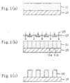
- the resist material having the aforementioned composition is applied by spin coating on a semiconductor substrate 10 , and the resultant is pre-baked, so as to form a resist film 11 with a thickness of 0.3 ⁇ m. Since the base polymer is alkali-refractory, the resist film 11 is alkali-refractory.
- the resist film 11 is irradiated through a mask 12 with F 2 excimer laser 13 for pattern exposure.
- the base polymer is decomposed by the F 2 excimer laser 13 in an exposed portion 11a of the resist film 11 , the exposed portion 11a becomes soluble in an alkaline developer while an unexposed portion 11b of the resist film 11 remains refractory in an alkaline developer.
- the resist film 11 is developed with an alkaline developer such as a tetramethylammonium hydroxide aqueous solution.
- an alkaline developer such as a tetramethylammonium hydroxide aqueous solution.
- the exposed portion 11a of the resist film 11 is dissolved in the developer, resulting in forming a resist pattern 14 from the unexposed portion 11b of the resist film 11 as is shown in Figure 1(c) .
- Embodiment 1 a methyl group is bonded to carbon located at the ⁇ -position and constituting the main chain of the base polymer, and the methyl group is never eliminated through the irradiation of the F 2 excimer laser 13 of a short wavelength. Accordingly, a crosslinking reaction of the main chain of the base polymer is never caused in the exposed portion 11a of the resist film 11 . As a result, the solubility of the base polymer in an alkaline developer can be improved.
- Embodiment 2 corresponds to the second pattern formation material and the second pattern formation method described above, and specifically, a pattern formation material including the following base polymer is used:
- Base polymer a polymer represented by Chemical Formula 3 2 g
- Acid generator triphenylsulfonium triflate 0.04 g
- Solvent diglyme 20 g
- R 0 and R 2 respectively correspond to R 0 and R 2 of General Formula 2 or 8
- R 3 and R 4 of General Formula 2 or 8 are both hydrogen in Chemical Formula 3.
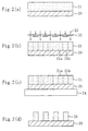
- the resist material having the aforementioned composition is applied by spin coating on a semiconductor substrate 20 , and the resultant is pre-baked, so as to form a resist film 21 with a thickness of 0.3 ⁇ m. Since the base polymer is alkali-refractory, the resist film 21 is alkali-refractory.
- the resist film 21 is irradiated through a mask 22 with F 2 excimer laser 23 for pattern exposure.
- an acid is generated from the acid generator in an exposed portion 21a of the resist film 21 while no acid is generated in an unexposed portion 21b of the resist film 21 .
- the semiconductor substrate 20 together with the resist film 21 are heated with a hot plate 24 .
- the exposed portion 21a of the resist film 21 becomes soluble in an alkaline developer because the acid generated from the acid generator decomposes the base polymer while the unexposed portion 21b of the resist film 21 remains refractory in an alkaline developer.
- the resist film 21 is developed with an alkaline developer such as a tetramethylammonium hydroxide aqueous solution.
- an alkaline developer such as a tetramethylammonium hydroxide aqueous solution.
- the exposed portion 21a of the resist film 21 is dissolved in the developer, resulting in forming a resist pattern 25 from the unexposed portion 21b of the resist film 21 as is shown in Figure 2(d) .
- a methyl group is bonded to carbon located at the ⁇ -position and constituting the main chain of the base polymer, and the methyl group is never eliminated through the irradiation of the F 2 excimer laser 23 of a short wavelength and the generation of the acid from the acid generator. Accordingly, the crosslinking reaction of the main chain of the base polymer is never caused in the exposed portion 21a of the resist film 21 . Accordingly, the solubility of the base polymer in an alkaline developer can be improved.
- R 0 of General Formula 1, 7, 2 or 8 is a methyl group, but the same effect can be attained by replacing the methyl group with another alkyl group such as an ethyl group.
- R 1 of General Formula 1, or 7 can be any group having at least one of an alkyl group, a carboxyl group, a carboxylic ester group, acetal, a group having an aliphatic ring, a group having an aromatic ring and a group having a hetero ring.
- R 2 of General Formula 2 or 8 can be any group having at least one of an alkyl group, a carboxyl group, a carboxylic ester group, acetal, a group having an aliphatic ring, a group having an aromatic ring and a group having a hetero ring, and examples are those represented by Chemical Formulas 4 and 5:
- R 3 and R 4 of General Formula 1, 7, 2 or 8 are not herein specified, and can be widely selected from hydrogen and compounds including hydrogen and carbon. Examples are an alkyl group such as a methyl group and an ethyl group, and a cyano group.
- Embodiment 3 corresponds to the third pattern formation material and the third pattern formation method described above, and is different from Embodiment 1 in the pattern formation material alone, and hence, the pattern formation material alone will be herein described.
- Base polymer a polymer represented by Chemical Formula 6 2 g
- Solvent diglyme 20 g
- R 0 and R 1 respectively correspond to R 0 and R 1 of General Formula 3 or 9, and R 3 and R 4 of General Formula 3 or 9 are both hydrogen in Chemical Formula 6.
- R 5 and R 6 of Chemical Formula 6 respectively correspond to R 5 and R 6 of General Formula 4 or 10, and R 7 and R 8 of General Formula 4 or 10 are both hydrogen in Chemical Formula 6.
- a methyl group is bonded to carbon located at the ⁇ -position and constituting the main chain of a first unit, and a methyl group is also bonded to carbon constituting the main chain of a second unit. Both the methyl groups are never eliminated through the irradiation of the F 2 excimer laser of a short wavelength, and hence, the crosslinking reaction of the main chain of the base polymer is never caused in an exposed portion of the resist film. Accordingly, the solubility of the exposed portion of the resist film in a developer can be improved in Embodiment 3.
- Embodiment 4 corresponds to the fourth pattern formation material and the fourth pattern formation method described above, and is different from Embodiment 2 in the pattern formation material alone, and hence, the pattern formation material alone will be herein described.
- Base polymer a polymer represented by Chemical Formula 7 2 g
- Acid generator triphenylsulfonium triflate 0.04 g
- Solvent diglyme 20 g
- R 0 and R 2 respectively correspond to R 0 and R 2 of General Formula 5 or 11, and R 3 and R 4 of General Formula 5 or 11 are both hydrogen in Chemical Formula 7.
- R 5 and R 6 of Chemical Formula 7 respectively correspond to R 5 and R 6 of General Formula 6 or 12, and R 7 and R 8 of General Formula 6 or 12 are both hydrogen in Chemical Formula 7.
- a methyl group is bonded to carbon located at the ⁇ -position and constituting the main chain of a first unit, and a methyl group is also bonded to carbon constituting the main chain of a second unit.
- Both the methyl groups are never eliminated through the irradiation of the F 2 excimer laser of a short wavelength and the generation of the acid from the acid generator, and hence, the crosslinking reaction of the main chain of the base polymer is never caused in an exposed portion of the resist film. Accordingly, the solubility of the exposed portion of the resist film in a developer can be improved in Embodiment 4.
- R 0 of General Formula 3, 9, 5 or 11 is a methyl group, but the same effect can be attained by replacing the methyl group with another alkyl group such as an ethyl group.
- R 1 of General Formula 3, or 9 can be any group having at least one of an alkyl group, a carboxyl group, a carboxylic ester group, acetal, a group having an aliphatic ring, a group having an aromatic ring and a group having a hetero ring.
- R 2 of General Formula 5 or 11 can be any group having at least one of an alkyl group, a carboxyl group, a carboxylic ester group, acetal, a group having an aliphatic ring, a group having an aromatic ring and a group having a hetero ring, and examples are those represented by Chemical Formulas 8 and 9:
- R 3 and R 4 of General Formula 3, 9, 5 or 11 and R 7 and R 8 of General Formula 4, 10, 6 or 12 are not herein specified, and can be widely selected from hydrogen and compounds including hydrogen and carbon. Examples are an alkyl group such as a methyl group and an ethyl group, and a cyano group.
Landscapes
- Physics & Mathematics (AREA)
- Spectroscopy & Molecular Physics (AREA)
- General Physics & Mathematics (AREA)
- Materials For Photolithography (AREA)
Priority Applications (1)
| Application Number | Priority Date | Filing Date | Title |
|---|---|---|---|
| EP03004858A EP1335246A1 (fr) | 1999-06-21 | 2000-06-20 | Matériau pour la formation de motifs |
Applications Claiming Priority (2)
| Application Number | Priority Date | Filing Date | Title |
|---|---|---|---|
| JP17420299 | 1999-06-21 | ||
| JP17420299 | 1999-06-21 |
Related Child Applications (1)
| Application Number | Title | Priority Date | Filing Date |
|---|---|---|---|
| EP03004858A Division EP1335246A1 (fr) | 1999-06-21 | 2000-06-20 | Matériau pour la formation de motifs |
Publications (1)
| Publication Number | Publication Date |
|---|---|
| EP1063567A1 true EP1063567A1 (fr) | 2000-12-27 |
Family
ID=15974516
Family Applications (2)
| Application Number | Title | Priority Date | Filing Date |
|---|---|---|---|
| EP03004858A Withdrawn EP1335246A1 (fr) | 1999-06-21 | 2000-06-20 | Matériau pour la formation de motifs |
| EP00112963A Withdrawn EP1063567A1 (fr) | 1999-06-21 | 2000-06-20 | Méthode et matériau pour la formation de motifs |
Family Applications Before (1)
| Application Number | Title | Priority Date | Filing Date |
|---|---|---|---|
| EP03004858A Withdrawn EP1335246A1 (fr) | 1999-06-21 | 2000-06-20 | Matériau pour la formation de motifs |
Country Status (2)
| Country | Link |
|---|---|
| US (1) | US6531259B1 (fr) |
| EP (2) | EP1335246A1 (fr) |
Families Citing this family (1)
| Publication number | Priority date | Publication date | Assignee | Title |
|---|---|---|---|---|
| US9077025B2 (en) | 2007-05-24 | 2015-07-07 | Nitto Denko Corporation | Method for production of porous film, porous film, separator for non-aqueous electrolyte battery, and non-aqueous electrolyte battery using the separator |
Citations (10)
| Publication number | Priority date | Publication date | Assignee | Title |
|---|---|---|---|---|
| JPS5639539A (en) * | 1979-09-07 | 1981-04-15 | Chiyou Lsi Gijutsu Kenkyu Kumiai | Pattern forming method |
| JPH02248952A (ja) * | 1989-03-22 | 1990-10-04 | Toshiba Corp | 感光性組成物 |
| EP0704762A1 (fr) * | 1994-09-02 | 1996-04-03 | Wako Pure Chemical Industries Ltd | Matériau pour réserve et formation de motifs structuraux |
| US5506088A (en) * | 1991-09-17 | 1996-04-09 | Fujitsu Limited | Chemically amplified resist composition and process for forming resist pattern using same |
| EP0780732A2 (fr) * | 1995-12-21 | 1997-06-25 | Wako Pure Chemical Industries Ltd | Composition à base de polymère et matériau pour réserve |
| EP0824223A1 (fr) * | 1996-08-15 | 1998-02-18 | Fuji Photo Film Co., Ltd. | Composition photosensible pour l'exposition avec des UV lointains |
| EP0875787A1 (fr) * | 1997-04-30 | 1998-11-04 | Wako Pure Chemical Industries, Ltd. | Méthode pour réduire la substrat-dépendance d'une réserver |
| US5863699A (en) * | 1995-10-12 | 1999-01-26 | Kabushiki Kaisha Toshiba | Photo-sensitive composition |
| US5908732A (en) * | 1996-09-23 | 1999-06-01 | International Business Machines Corporation | Polymer compositions for high resolution resist applications |
| EP1035441A1 (fr) * | 1999-03-09 | 2000-09-13 | Matsushita Electric Industrial Co., Ltd. | Procédé pour la formation de motifs |
Family Cites Families (11)
| Publication number | Priority date | Publication date | Assignee | Title |
|---|---|---|---|---|
| JPS58114033A (ja) * | 1981-12-28 | 1983-07-07 | Fujitsu Ltd | パタ−ン形成方法 |
| JPH03223861A (ja) | 1990-01-30 | 1991-10-02 | Wako Pure Chem Ind Ltd | 新規なレジスト材料 |
| JPH0777799A (ja) * | 1993-03-30 | 1995-03-20 | Nippon Zeon Co Ltd | レジスト組成物 |
| JP3203995B2 (ja) * | 1993-12-24 | 2001-09-04 | ジェイエスアール株式会社 | 感放射線性樹脂組成物 |
| US5861231A (en) | 1996-06-11 | 1999-01-19 | Shipley Company, L.L.C. | Copolymers and photoresist compositions comprising copolymer resin binder component |
| JP3674243B2 (ja) * | 1997-05-21 | 2005-07-20 | Jsr株式会社 | レジストパターン形成方法 |
| JPH11231536A (ja) | 1998-02-10 | 1999-08-27 | Fuji Photo Film Co Ltd | ポジ型感光性組成物 |
| JPH11231537A (ja) | 1998-02-16 | 1999-08-27 | Fuji Photo Film Co Ltd | ポジ型感光性組成物 |
| JP3281612B2 (ja) * | 1999-03-05 | 2002-05-13 | 松下電器産業株式会社 | パターン形成方法 |
| US6280908B1 (en) * | 1999-04-15 | 2001-08-28 | International Business Machines Corporation | Post-development resist hardening by vapor silylation |
| JP2001066780A (ja) * | 1999-06-21 | 2001-03-16 | Matsushita Electric Ind Co Ltd | パターン形成方法 |
-
2000
- 2000-06-13 US US09/592,937 patent/US6531259B1/en not_active Expired - Lifetime
- 2000-06-20 EP EP03004858A patent/EP1335246A1/fr not_active Withdrawn
- 2000-06-20 EP EP00112963A patent/EP1063567A1/fr not_active Withdrawn
Patent Citations (10)
| Publication number | Priority date | Publication date | Assignee | Title |
|---|---|---|---|---|
| JPS5639539A (en) * | 1979-09-07 | 1981-04-15 | Chiyou Lsi Gijutsu Kenkyu Kumiai | Pattern forming method |
| JPH02248952A (ja) * | 1989-03-22 | 1990-10-04 | Toshiba Corp | 感光性組成物 |
| US5506088A (en) * | 1991-09-17 | 1996-04-09 | Fujitsu Limited | Chemically amplified resist composition and process for forming resist pattern using same |
| EP0704762A1 (fr) * | 1994-09-02 | 1996-04-03 | Wako Pure Chemical Industries Ltd | Matériau pour réserve et formation de motifs structuraux |
| US5863699A (en) * | 1995-10-12 | 1999-01-26 | Kabushiki Kaisha Toshiba | Photo-sensitive composition |
| EP0780732A2 (fr) * | 1995-12-21 | 1997-06-25 | Wako Pure Chemical Industries Ltd | Composition à base de polymère et matériau pour réserve |
| EP0824223A1 (fr) * | 1996-08-15 | 1998-02-18 | Fuji Photo Film Co., Ltd. | Composition photosensible pour l'exposition avec des UV lointains |
| US5908732A (en) * | 1996-09-23 | 1999-06-01 | International Business Machines Corporation | Polymer compositions for high resolution resist applications |
| EP0875787A1 (fr) * | 1997-04-30 | 1998-11-04 | Wako Pure Chemical Industries, Ltd. | Méthode pour réduire la substrat-dépendance d'une réserver |
| EP1035441A1 (fr) * | 1999-03-09 | 2000-09-13 | Matsushita Electric Industrial Co., Ltd. | Procédé pour la formation de motifs |
Non-Patent Citations (2)
| Title |
|---|
| PATENT ABSTRACTS OF JAPAN vol. 005, no. 096 (P - 067) 23 June 1981 (1981-06-23) * |
| PATENT ABSTRACTS OF JAPAN vol. 014, no. 577 (P - 1146) 21 December 1990 (1990-12-21) * |
Also Published As
| Publication number | Publication date |
|---|---|
| EP1335246A1 (fr) | 2003-08-13 |
| US6531259B1 (en) | 2003-03-11 |
Similar Documents
| Publication | Publication Date | Title |
|---|---|---|
| JPH07261393A (ja) | ネガ型レジスト組成物 | |
| US6632582B2 (en) | Pattern formation material and pattern formation method | |
| US6753132B2 (en) | Pattern formation material and pattern formation method | |
| US6521393B1 (en) | Pattern formation method | |
| EP1295177B1 (fr) | Compositions de resine de generateur d'acide photosensible fortement hydrosolubles | |
| US6475706B1 (en) | Pattern formation method | |
| EP1063567A1 (fr) | Méthode et matériau pour la formation de motifs | |
| US20040029035A1 (en) | Pattern-forming material and method of forming pattern | |
| US6764811B2 (en) | Pattern formation method | |
| US6511786B2 (en) | Pattern formation material and pattern formation method | |
| US6645694B2 (en) | Pattern formation material and pattern formation method | |
| US6830869B2 (en) | Pattern forming material and method of pattern formation | |
| US6689536B2 (en) | Pattern formation material and pattern formation method | |
| EP1148388A1 (fr) | Matériau et procédé pour la formation de motifs | |
| US6737213B2 (en) | Pattern formation material and method | |
| US20030091930A1 (en) | Pattern formation material and pattern formation method | |
| US6444395B1 (en) | Pattern formation material and method | |
| US6528240B1 (en) | Pattern formation method | |
| US6576398B2 (en) | Pattern formation material and method | |
| JP3285854B2 (ja) | パターン形成方法 | |
| JPH05323590A (ja) | 化学増幅型レジスト組成物 | |
| US6537736B1 (en) | Patten formation method | |
| KR100209371B1 (ko) | 원자외선용 감광막과 반도체소자의 미세패턴 형성방법 | |
| JP2000330288A (ja) | パターン形成方法 |
Legal Events
| Date | Code | Title | Description |
|---|---|---|---|
| PUAI | Public reference made under article 153(3) epc to a published international application that has entered the european phase |
Free format text: ORIGINAL CODE: 0009012 |
|
| AK | Designated contracting states |
Kind code of ref document: A1 Designated state(s): DE FR GB NL |
|
| AX | Request for extension of the european patent |
Free format text: AL;LT;LV;MK;RO;SI |
|
| 17P | Request for examination filed |
Effective date: 20010518 |
|
| AKX | Designation fees paid |
Free format text: DE FR GB NL |
|
| 17Q | First examination report despatched |
Effective date: 20020827 |
|
| RIN1 | Information on inventor provided before grant (corrected) |
Inventor name: SASAGO, MASARU Inventor name: KATSUYAMA, AKIKO Inventor name: KISHIMURA, SHINJI |
|
| 17Q | First examination report despatched |
Effective date: 20020827 |
|
| STAA | Information on the status of an ep patent application or granted ep patent |
Free format text: STATUS: THE APPLICATION IS DEEMED TO BE WITHDRAWN |
|
| 18D | Application deemed to be withdrawn |
Effective date: 20070220 |