EP1063578B1 - Générateur de tension de référence avec dispositif de surveillance et de mise en marche - Google Patents
Générateur de tension de référence avec dispositif de surveillance et de mise en marche Download PDFInfo
- Publication number
- EP1063578B1 EP1063578B1 EP99401555A EP99401555A EP1063578B1 EP 1063578 B1 EP1063578 B1 EP 1063578B1 EP 99401555 A EP99401555 A EP 99401555A EP 99401555 A EP99401555 A EP 99401555A EP 1063578 B1 EP1063578 B1 EP 1063578B1
- Authority
- EP
- European Patent Office
- Prior art keywords
- voltage
- coupled
- terminal
- output terminal
- monitoring means
- Prior art date
- Legal status (The legal status is an assumption and is not a legal conclusion. Google has not performed a legal analysis and makes no representation as to the accuracy of the status listed.)
- Expired - Lifetime
Links
- 238000012544 monitoring process Methods 0.000 title claims abstract description 55
- 238000010200 validation analysis Methods 0.000 claims abstract description 10
- 238000013475 authorization Methods 0.000 claims description 13
- 230000008878 coupling Effects 0.000 claims description 4
- 238000010168 coupling process Methods 0.000 claims description 4
- 238000005859 coupling reaction Methods 0.000 claims description 4
- 230000003213 activating effect Effects 0.000 claims 1
- HBBGRARXTFLTSG-UHFFFAOYSA-N Lithium ion Chemical compound [Li+] HBBGRARXTFLTSG-UHFFFAOYSA-N 0.000 description 1
- 230000003321 amplification Effects 0.000 description 1
- 238000005094 computer simulation Methods 0.000 description 1
- 238000010586 diagram Methods 0.000 description 1
- 231100001261 hazardous Toxicity 0.000 description 1
- 230000010354 integration Effects 0.000 description 1
- 229910001416 lithium ion Inorganic materials 0.000 description 1
- 230000007257 malfunction Effects 0.000 description 1
- 238000003199 nucleic acid amplification method Methods 0.000 description 1
- 238000004513 sizing Methods 0.000 description 1
Images

Classifications
-
- G—PHYSICS
- G05—CONTROLLING; REGULATING
- G05F—SYSTEMS FOR REGULATING ELECTRIC OR MAGNETIC VARIABLES
- G05F1/00—Automatic systems in which deviations of an electric quantity from one or more predetermined values are detected at the output of the system and fed back to a device within the system to restore the detected quantity to its predetermined value or values, i.e. retroactive systems
- G05F1/10—Regulating voltage or current
- G05F1/46—Regulating voltage or current wherein the variable actually regulated by the final control device is DC
- G05F1/56—Regulating voltage or current wherein the variable actually regulated by the final control device is DC using semiconductor devices in series with the load as final control devices
- G05F1/575—Regulating voltage or current wherein the variable actually regulated by the final control device is DC using semiconductor devices in series with the load as final control devices characterised by the feedback circuit
-
- G—PHYSICS
- G05—CONTROLLING; REGULATING
- G05F—SYSTEMS FOR REGULATING ELECTRIC OR MAGNETIC VARIABLES
- G05F3/00—Non-retroactive systems for regulating electric variables by using an uncontrolled element, or an uncontrolled combination of elements, such element or such combination having self-regulating properties
- G05F3/02—Regulating voltage or current
- G05F3/08—Regulating voltage or current wherein the variable is DC
- G05F3/10—Regulating voltage or current wherein the variable is DC using uncontrolled devices with non-linear characteristics
- G05F3/16—Regulating voltage or current wherein the variable is DC using uncontrolled devices with non-linear characteristics being semiconductor devices
- G05F3/20—Regulating voltage or current wherein the variable is DC using uncontrolled devices with non-linear characteristics being semiconductor devices using diode- transistor combinations
- G05F3/30—Regulators using the difference between the base-emitter voltages of two bipolar transistors operating at different current densities
Definitions
- the present invention relates to a voltage reference generator as is described in the preamble of the first claim.
- Such a voltage reference generator is already known in the art, e.g. from the US patent 5 867 013.
- a voltage reference generator is shown, including start-up means, an input terminal of which is coupled to an output terminal of the operational amplifier of the bandgap reference circuit, and which is adapted to compare the voltage signal at the output terminal of the bandgap reference circuit, with a start-up threshold.
- This prior art startup circuit further includes second circuitry responsive to the result of the aforementioned comparison such as to provide a second input voltage to the operational amplifier of the bandgap reference.
- Such a prior art start-up circuit can guarantee a stable operation point of the bandgap reference circuit.
- An object of the present invention is thus to provide a voltage reference generator of the above known kind, but which solves the aforementioned problems.
- the voltage reference generator further includes the features as described by the characteristic portion of the first claim.
- the second output terminal of the monitoring means provides a validation flag indicative of the correct and reliable operation of the voltage reference generator, which can thus be interpreted by further circuitry. Furthermore, by simultaneously monitoring two parameters of the operational amplifier means, a better, more accurate and full-proof indication of the correctness of the operation is obtained compared to the case where only one single parameter, as in the prior art case, is monitored. As will become clear from the descriptive part of this document, very simple embodiments are possible for realising these characteristic features such that the resulting voltage reference generator is at the same time very accurate and yet simple to realise.
- the second parameter thus consists of a current flowing through an output stage of the operational amplifier means. Comparison of this value with a predetermined threshold current level, results in a first authorisation flag, being an internal signal of said monitoring means. Thereby a first indication of the correct operation of the circuit is provided.
- the reference output voltage is compared to a predetermined threshold voltage level within a voltage monitoring means. This results in a second indication of the correct operation of the circuit.
- an AND-type means is a simple means for guaranteeing that both authorisation flags simultaneously have to comply to certain values, such that an unambiguous validation flag is provided to the second output terminal of the voltage reference generator.
- the value of the predetermined threshold voltage level with which the reference output voltage is compared is a design parameter related to the stable operating point, as is stated in claim 6. This will also be further explained in the descriptive part of this document.
- the output stage of the operational amplifier means and the current monitoring means are thereby similar in structure, consisting of a current source in series with an active element, for instance a transistor. Both transistors are grounded and controlled by the same signal, which is delivered at the second output terminal of the operational amplifier means.
- the transistors of the output stage and the current monitor such that their current ratio equals the ratio of a first current and a second current, this first current being related to the current supplied by the first current source, this second current being the current delivered by the second current source, the current comparison function of the current monitor means is obtained.
- the current monitor means has to check whether the current flowing through the output stage exceeds a predetermined threshold current level. This current flowing through the output stage is the current that flows when the first transistor is on.
- the first current is thereby equal to the current delivered by the first current source, minus the current delivered to the feedback circuit, in the stable operating region, and minus a predetermined current to a load.
- the first transistor When the first transistor is on, it will thus carry the first current. Since the first and second transistors both receive the same driving signal, and since the ratios of their currents match with the ratio of the first and second currents, the output of the current monitor indicates whether the first current is sunk by the first transistor, thereby thus providing the current comparison function envisaged.
- Bandgap voltage reference generators such as the voltage reference generator VRG of the present invention are widely used in electronics, in all cases where a fully integrated, precise and stable voltage reference is needed. This is a very general need in analog integrated circuits such as analog/digital or digital/analog converters, supply regulators, level detectors, power-on reset functions, analog timers, charger circuits, etc.
- Bandgap voltage reference generators are known for a long time and extensively described in the specialised literature, such as in the referenced prior art document.
- a bandgap voltage reference circuit consisting of an operational amplifier means, and a feedback means, as is shown in their figure 4.49c, may have several operating points. This is highly undesirable, and provisions have to be taken in order to guarantee operation in only one of these points.
- an indication is to be foreseen as to the validity of the bandgap output signal. Indeed, in case the circuit is still not in its desired stable operating point, the value of the provided output voltage reference signal may be wrong.
- the complete circuit still needs to be small for integration, especially e.g. into a GSM integrated circuit, where each ⁇ m2 is important.
- the bandgap voltage reference circuit of the present invention fulfills the aforementioned requirements.
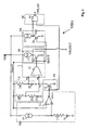
- a basic scheme is shown in Fig. 1, wherein a voltage reference generator VRG is depicted. It includes a supply voltage terminal, denoted VDD, for coupling to a power supply, having a value of for instance 3.3 V, and a reference terminal, denoted VSS, for coupling to a reference potential, for instance the ground reference.
- This voltage reference generator further includes an operational amplifier means, denoted 7, of which a first, respectively a second input terminal, NA, resp. NB, are coupled to two output terminals of a feedback circuit, denoted 8.
- An input terminal of the feedback circuit is coupled to a first amplifier output terminal, denoted VOAOUT, of the operational amplifier means 7.
- This first amplifier output terminal VOAOUT is also coupled to a first output terminal VBGOUT of the voltage reference generator and provides the reference output voltage, hereafter denoted VBG.
- the voltage reference generator further includes a start-up means, 10, of which the operation is controlled by a first output signal provided by a monitoring means, denoted 9.
- This first output signal is provided at a first output terminal VOUT1 of this monitoring means, the control terminal of the start-up means 9 is denoted VC.
- An output terminal, denoted VO, of the start-up means is coupled to the second input terminal of the operational amplifier means 7, thereby controlling its operation.
- a third terminal of the start-up means is coupled to the reference terminal VSS.
- the monitoring means 9 is further coupled between the supply and the reference terminals, VDD, resp. VSS, and includes two input terminals, a first one being coupled to the first ouput terminal VOAOUT of the operational amplifier means 7, and a second one coupled to a second output terminal, denoted ISOUT, of the operational amplifier means 7.
- this monitoring means includes a second output terminal, denoted VOUT2, which provides a validation flag, the value of which is indicative of a correct value of the reference output voltage VBG.
- This second output terminal VOUT2 is coupled to a second output terminal, denoted VFLAG, of the voltage reference generator itself. At this output terminal, the indication of the correct operation of the complete structure is thus provided by means of a validation flag .
- the monitoring means further includes 3 main building blocks : a current monitoring means, denoted 9A, a voltage monitoring means, denoted 9B, and an AND-type means, denoted 9C.
- the current monitoring means 9A includes an input terminal which is coupled to the second input terminal of the monitoring means, and consequently to the second output terminal ISOUT of the operational amplifier means 7.
- the current monitoring means is adapted to compare a first current flowing internally through an output stage of the operational amplifier means, thus from the supply to the reference terminal, with a predetermined threshold current level. Thereby an output signal at an output terminal, denoted CMO, is provided, this output signal corresponding to a first authorisation flag in case this first current exceeds this predetermined threshold current level. How this is performed will be described in a further paragraph of this document.
- the voltage monitoring means includes an input terminal which is coupled to the first input terminal of the monitoring means, and consequently to the first amplifier output terminal VOAOUT of the operational amplifier means. It further includes an output terminal which is coupled to the first output terminal VOUT1 of the monitoring means.
- the voltage monitoring means is adapted to compare the signal provided at VOAOUT, being the reference output voltage VBG, with a predetermined threshold voltage level, the result of the comparison being the signal provided at terminal VOUT1.
- the latter signal being such that in case VBG exceeds the predetermined threshold voltage level, the start-up means is not activated while the level of the signal itself provides a second authorisation flag.
- the output signal is such that the start-up means is activated, while at the same time having a logical level such that the second authorisation flag is not provided.
- AND-type means are such that both authorisation flags are to be simultaneously present in order to obtain a valid output signal.
- the output terminal of the AND-type means is coupled to the second output terminal VOUT2 of the monitoring means; the signal provided thereon thus being indicative of a simultaneous compliance of both the sensed current and the sensed voltage with the criterion of being larger than the predetermined threshold current, resp. voltage. Since this signal also corresponds to the validation flag, provided at terminal VFLAG, two parameters of the operational amplifier means are thus monitored for providing an indication of the correct operation.
- the reference terminal VSS corresponds to the ground terminal, as is as such depicted.
- the operational amplifier means 7 of Fig. 2 consists of an input amplifier stage 12, having a first and a second input terminal, respectively denoted with - and + and respectively coupled to the first NA and second NB input terminal of the operational amplifier means.
- the input amplifier stage further includes an output terminal , which is coupled to the second amplifier output terminal ISOUT.
- this input amplifier stage is as well coupled between the VDD and the ground terminal.
- the second output terminal ISOUT of the amplifier means is coupled to a control input terminal of an output stage denoted 30, also included in the operational amplifier means 7.
- This output stage 30 consists of a first current source 13 in series with a first transistor 22, and coupled between the power supply terminal VDD and the ground reference terminal.
- the control terminal of the first transistor 22 is coupled to the output terminal of the input amplifier stage, whereas the intersection point between the first current source 13 and the conductive path of the first transistor, constitutes the first amplifier output terminal VOAOUT, which also constitutes the first output terminal VBGOUT of the embodiment of the voltage reference generator depicted in Fig. 2.
- the feedback circuit 8 of Fig. 2 corresponds to the one referred to in the prior art document. It is coupled in a feedback configuration between the first amplifier output terminal VOAOUT, and both input terminals NA and NB of the operational amplifier means.
- Feedback circuit 8 includes resistor 24, coupled between VOAOUT and NA, whereby the latter junction point to NA is also further coupled via a diode 25 to the ground terminal.
- Feedback circuit 8 also includes two other resistors 20 and 21, the intersection point between them being coupled to NB, the other terminal of resistor 20 being coupled to VOAOUT, and the other terminal of resistor 21 being as well coupled to the ground terminal via another diode 23.
- the operation of the combination of an amplifier means and a feedback circuit as depicted in the embodiment of Fig. 2 is common prior art knowlegde concerning bandgap voltage generators, and will therefore not be discussed in this document.
- Current monitoring means 9A has a structure similar to the output stage 30 of the operational amplifier means 7 . It includes a second current source 27 coupled in series with a second transistor 26 between the supply voltage terminal VDD and the ground reference terminal. The control terminal of the second transistor 26 is as well coupled to the second output terminal ISOUT of the amplifier means. This means that both first and second transistors are driven by the same voltage. By virtue of the operation of transistor 22, the value of this voltage relates to the current flowing through the output stage 30, in between VDD and the ground terminal. Indeed, in case the voltage at terminal ISOUT is lower than the threshold voltage of transistor 22, all current provided by current source 13 is fed to the feedback circuit 8 and possibly to a load coupled to output terminal VGBOUT (this load is not shown on Fig.
- Transistors 26 and 22 are designed such that the currents they carry comply with a predetermined ratio. In case of MOS transistors such as shown in Fig. 2, this is accomplished by means of selecting the width/length ratios of these transistors to match this predetermined ratio. In case of bipolar transistors, this is for instance accomplished by a sizing in the area of their emitters.
- This predetermined ratio is thereby the same as the one between a first current related to the current supplied by the first current source, and a second current, which is supplied by the second current source.
- the first current is thereby equal to the current supplied by the first current source, minus the current flowing in the feedback circuit in the stable operating point of the voltage reference generator, and minus the current flowing through a load coupled to the first output terminal VBGOUT (this load is not shown on Fig. 2).
- the start-up means 10 consists of an active device, for instance a transistor such as transistor 11, having a control terminal, in the embodiment of Fig. 2 constituting the control terminal VC of the start-up means.
- the conductive path of transistor 11 is coupled between the output terminal VO of the start-up means and the ground reference terminal.
- transistor 11 consists of a nMOS transistor
- the output terminal VO of the start-up means which is further coupled to input terminal NB of the operational amplifier means, corresponds to the drain terminal of this transistor.
- the AND-means 9C corresponds to a NAND-gate 19. This means that the output signal generated by it will only have a logical "high” value, in case its inputs both have a logical "low” or "zero” value.
- the voltage monitoring means 9B mainly consists of a comparator, which, in the embodiment depicted in Fig. 2, consists of another operational amplifier 15.
- This comparator receives at its negative input terminal the voltage provided at the first output terminal VOAOUT of the operational amplifier means 7, and at its positive input terminal a predetermined threshold voltage which is generated by the series connection of a third current source 18, a resistor 17 and a diode, coupled between the supply voltage terminal VDD and the ground terminal.
- This series connection thereby constitutes a threshold voltage providing means.
- the value of the predetermined threshold voltage provided by this threshold voltage providing means is selected such as to lie in between the desired stable operating point, and its closest lower metastable operating point of the voltage reference generator, and taken into account all possible temperature and processing variations of the constituting components.
- a threshold voltage of 0.9 V in chosen as lying in between both values, thereby taking into account these fluctuations in temperature, processing, etc.
- This value of 0.9 V is then obtained by selecting the current through 18 and the value of resistor 17 to be such that their product equals 0.3 V, provided that the built-in forward junction voltage of diode 16 is 0.6 V.
- amplifier 15 is a differential amplifier with a high amplification factor, the difference between voltage at its input, corresponding to the difference between VBG, and this predetermined threshold voltage, is amplified, thereby providing an output signal at VOUT1.
- the current monitoring circuit 9A realises a current comparator function, generating a digital output signal at CMO.
- the CMO output of the current comparator is pulled up to VDD (high digital level). Because the width/length ratios between transistors 26 and 22, and consequently their saturation currents they carry, correspond to the ratios between the second and first currents, CMO being pulled high indicates as well that still most current sourced by 13, into the output stage of the amplifier 7, is flowing into the feedback network, and possibly to the load (not shown in Fig. 2), thereby trying to raise the VBG output voltage at output terminal VBGOUT.
- the start-up means releases the internal voltage reference circuit consisting of amplifier means 7 and feedback circuit 8, because now it is guaranteed that the VBG voltage has passed all undesired (meta)stable operating points, and can only evolve to the final VBG level of for instance 1.2V.
- the actual core of the reference voltage generator (7 and 8) is now allowed to 'settle'. While it is doing so, it will gradually turn on transistor 22 in the output stage. This is where the current monitoring comes into the picture, because this will now detect a certain amount of current flowing through transistor 22, high enough to ensure that the feedback loop is completely in regulation, and hence the output reference voltage VBGOUT is within a predetermined percentage, for instance 0.5% ,of its final accuracy.
- the AND-means consisting of the NAND-gate 19 thereby checks the presence of two logical low values, one delivered by the current monitoring means and consisting of a first authorisation flag, a second by the voltage monitoring means and consisting of a second authorisation flag. When both flags are present, the output of the NAND-gate has a logical high-value and provides the final validation flag, indicative of the correct operation of the voltage reference generator.
Landscapes
- Engineering & Computer Science (AREA)
- Physics & Mathematics (AREA)
- Microelectronics & Electronic Packaging (AREA)
- Radar, Positioning & Navigation (AREA)
- Automation & Control Theory (AREA)
- Electromagnetism (AREA)
- General Physics & Mathematics (AREA)
- Nonlinear Science (AREA)
- Power Engineering (AREA)
- Continuous-Control Power Sources That Use Transistors (AREA)
- Control Of Electrical Variables (AREA)
- Control Of Charge By Means Of Generators (AREA)
- Control Of Voltage And Current In General (AREA)
- Control Of Eletrric Generators (AREA)
- Power Steering Mechanism (AREA)
- Details Of Television Scanning (AREA)
- Semiconductor Integrated Circuits (AREA)
Claims (10)
- Générateur de référence de tension (VRC) comprenant une borne de tension d'alimentation (VDD) pour le couplage à une alimentation, une borne de référence (VSS) pour le couplage à un potentiel de référence, des moyens formant amplificateur opérationnel (7) comportant une première borne d'entrée (NA), une deuxième borne d'entrée (NB) et une première borne de sortie d'amplificateur (VOAOUT) qui est couplée à une borne d'entrée d'un circuit de rétroaction (8) dudit générateur de référence de tension, ledit générateur de référence de tension (VRG) comprenant une première borne de sortie (VBGOUT) couplée à ladite première borne de sortie d'amplificateur (VOAOUT) pour fournir une tension de sortie de référence,caractérisé en ce queledit générateur de référence de tension comprend en outre des moyens de surveillance (9), adaptés pour surveiller ladite tension de sortie de référence, une première borne d'entrée desdits moyens de surveillance étant, de ce fait, couplée à ladite première borne de sortie d'amplificateur (VOAOUT),lesdits moyens de surveillance (9) comprenant, de ce fait, une première borne de sortie (VOUT1) qui est couplée à une borne de commande (VC) de moyens de démarrage (10) compris en outre dans ledit générateur de référence de tension (VRG), lesdits moyens de démarrage (10) comprenant une borne de sortie (VO) qui est couplée à ladite deuxième borne d'entrée (NB) desdits moyens formant amplificatcur opérationnel (7),lesdits moyens de surveillance (9) comprennent une deuxième borne de sortie (VOUT2) couplée à une deuxième borne de sortie (VELAG) dudit générateur de référence de tension (VRG) pour la fourniture d'un indicateur de validation indicatif du fonctionnement correct dudit générateur de référence de tension, etlesdits moyens de surveillance (9) sont en outre adaptés pour surveiller simultanément ladite tension de sortie de référence et un deuxième paramètre desdits moyens formant amplificateur opérationnel (7), une valeur liée audit deuxième paramètre étant, de ce fait, fournie à une deuxième borne de sortie (ISOUT) desdits moyens formant amplificateur opérationnel (7) qui est en outre couplée à une deuxième borne d'entrée desdits moyens de surveillance (9).
- Générateur de référence de tension (VRG) selon la revendication 1,
caractérisé en ce que
lesdits moyens de surveillance (9) comprennent en outre des moyens de surveillance de courant (9A) dont une borne d'entrée est couplée à ladite deuxième borne d'entrée desdits moyens de surveillance (9), lesdits moyens de surveillance de courant (9A) étant adaptés pour fournir un premier indicateur d'autorisation à une borne de sortie de surveillance de courant (CMO) dès qu'un courant circulant à travers un étage de sortie (30) desdits moyens formant amplificateur opérationnel (7), qui constitue ledit deuxième paramètre, dépasse un niveau de courant de seuil prédéterminé. - Générateur de référence de tension (VRG) selon la revendication 1,
caractérisé en ce que
lesdits moyens de surveillance (9) comprennent en outre des moyens de surveillance de tension (9B), dont une borne d'entrée est couplée à ladite première borne d'entrée desdits moyens de surveillance (9), lesdits moyens de surveillance de tension (9B) étant adaptés pour fournir un deuxième indicateur d'autorisation à une borne de sortie couplée à ladite première borne de sortie (VOUT1) desdits moyens de surveillance (9) lorsque ladite tension de sortie de référence dépasse un niveau de tension de seuil prédéterminé, et pour activer lesdits moyens de démarrage en fournissant un signal à ladite première borne de sortie desdits moyens de surveillance (9) lorsque ladite tension de sortie de référence est Inférieure ou égale audit niveau de tension de seuil prédéterminé. - Générateur de référence de tension (VRG) selon les revendications 2 ct 3,
caractérisé en ce que
lesdits moyens de surveillance (9) comprennent en outre des moyens de type ET (9C), dont une première borne d'entrée est couplée à ladite borne de sortie desdits moyens de surveillance de tension (9B), dont une deuxième borne d'entrée est couplée à ladite borne de sortie de surveillance de courant (CMO), lesdits moyens de type ET étant adaptés pour fournir ledit indicateur de validation à une borne de sortie couplée à ladite deuxième borne de sortie (VOUT2) desdits moyens de surveillance (9) lorsque lesdits moyens de type ET reçoivent simultanément lesdits premier et deuxième indicateurs d'autorisation. - Générateur de référence de tension (VRG) selon la revendication 3,
caractérisé en ce que
lesdits moyens de surveillance de tension (9B) comprennent en outre un comparateur (15) avec une première borne d'entrée de comparateur couplée à ladite première borne de sortie d'amplificateur (VOAOUT), une deuxième borne d'entrée de comparateur couplée à des moyens de fourniture de tension de seuil (16, 17, 18) adaptés pour fournir ledit niveau de tension de seuil prédéterminé, et une borne de sortie de comparateur couplée à ladite première borne de sortie (VOUT1) desdits moyens de surveillance (9), ledit comparateur étant adapté pour fournir ledit indicateur d'autorisation de tension à ladite borne de sortie de comparateur lorsque ladite tension de sortie de référence dépasse ledit niveau de tension de seuil prédéterminé et pour fournir un signal à ladite borne de sortie de comparateur pour activer lesdits moyens de démarrage (10) tant que ladite tension de sortie de référence est inférieure à cette tension de seuil prédéterminée. - Générateur de référence de tension (VRG) selon la revendication 5,
caractérisé en ce que
ledit niveau de tension de seuil prédéterminé détermine de façon unique un point de fonctionnement stable dudit générateur de référence de tension. - Générateur de référence de tension (VRG) selon la revendication 1,
caractérisé en ce que
lesdits moyens de démarrage (10) comprennent un dispositif actif (11) dont une borne de commande est couplée à ladite borne de commande (VC) desdits moyens de démarrage (10), dont un trajet conducteur est couplé entre ladite borne de sortie (VO) desdits moyens de démarrage (10) et ladite borne de référence (VSS). - Générateur de référence de tension (VRG) selon la revendication 1,
caractérisé en ce que
lesdits moyens formant amplificateur opérationnel (7) comprennent en outre un étage d'amplification d'entrée, une première, respectivement une deuxième borne d'entrée de celui-ci étant respectivement couplée à ladite première (NA), respectivement deuxième (NB) borne d'entrée desdits moyens formant amplificateur opérationnel, une borne de sortie de celui-ci constituant ladite deuxième borne de sortie (ISOUT) desdits moyens formant amplificateur opérationnel (7). - Générateur de référence de tension (VRG) selon la revendication 2,
caractérisé en ce que
ledit étage de sortie (30) de ladite unité d'amplificateur opérationnel (7) comprend une première source de courant (13) en série avec un premier transistor (22), dont une borne de commande est couplée à ladite deuxième borne de sortie (ISOUT) desdits moyens formant amplificateur opérationnel (7), dont un trajet conducteur commandé est couplé entre ladite première borne de sortie d'amplificateur (VOAOUT) et ladite borne de référence (VSS). - Générateur de référence de tension (VRG) selon la revendication 9,
caractérisé en ce que
lesdits moyens de surveillance de courant (9A) comprennent en outre une deuxième source de courant couplée entre ladite borne de tension d'alimentation (VDD) et ladite borne de sortie (CMO) desdits moyens de surveillance de courant (9A), lesdits moyens de surveillance de courant (9A) comprennent en outre un deuxième transistor (26), dont une borne de commande est couplée à ladite deuxième borne de sortie (ISOUT) desdits moyens formant amplificateur opérationnel (7), dont un trajet conducteur commandé est couplé entre ladite borne de sortie (CMO) desdits moyens de surveillance de courant (9A) et ladite borne de référence (VSS).
Priority Applications (12)
| Application Number | Priority Date | Filing Date | Title |
|---|---|---|---|
| AT99401555T ATE224073T1 (de) | 1999-06-22 | 1999-06-22 | Referenzspannungsgenerator mit überwachungs- und anlaufschaltung |
| ES99401555T ES2180257T3 (es) | 1999-06-22 | 1999-06-22 | Generador de tension de referencia con medios de vigilancia y puesta en marcha. |
| EP99401555A EP1063578B1 (fr) | 1999-06-22 | 1999-06-22 | Générateur de tension de référence avec dispositif de surveillance et de mise en marche |
| DE69902891T DE69902891T2 (de) | 1999-06-22 | 1999-06-22 | Referenzspannungsgenerator mit Überwachungs- und Anlaufschaltung |
| TW089103269A TW459170B (en) | 1999-06-22 | 2000-02-24 | Reference voltage generator with monitoring and start up means |
| AU34028/00A AU3402800A (en) | 1999-06-22 | 2000-05-10 | Reference voltage generator with monitoring and start up means |
| IL13614000A IL136140A0 (en) | 1999-06-22 | 2000-05-15 | Reference voltage generator with monitoring and start up means |
| JP2000171613A JP2001042960A (ja) | 1999-06-22 | 2000-06-08 | モニタ手段およびスタートアップ手段を有する基準電圧発生器 |
| CA002311069A CA2311069A1 (fr) | 1999-06-22 | 2000-06-09 | Generateur de tension de reference avec outils de surveillance et d'activation |
| US09/595,905 US6204653B1 (en) | 1999-06-22 | 2000-06-20 | Reference voltage generator with monitoring and start up means |
| KR1020000034431A KR20010007480A (ko) | 1999-06-22 | 2000-06-22 | 모니터링 및 개시 수단을 갖는 기준 전압 발생기 |
| SG200003515A SG84607A1 (en) | 1999-06-22 | 2000-06-22 | Reference voltage generator with monitoring and start up means |
Applications Claiming Priority (1)
| Application Number | Priority Date | Filing Date | Title |
|---|---|---|---|
| EP99401555A EP1063578B1 (fr) | 1999-06-22 | 1999-06-22 | Générateur de tension de référence avec dispositif de surveillance et de mise en marche |
Publications (2)
| Publication Number | Publication Date |
|---|---|
| EP1063578A1 EP1063578A1 (fr) | 2000-12-27 |
| EP1063578B1 true EP1063578B1 (fr) | 2002-09-11 |
Family
ID=8242019
Family Applications (1)
| Application Number | Title | Priority Date | Filing Date |
|---|---|---|---|
| EP99401555A Expired - Lifetime EP1063578B1 (fr) | 1999-06-22 | 1999-06-22 | Générateur de tension de référence avec dispositif de surveillance et de mise en marche |
Country Status (12)
| Country | Link |
|---|---|
| US (1) | US6204653B1 (fr) |
| EP (1) | EP1063578B1 (fr) |
| JP (1) | JP2001042960A (fr) |
| KR (1) | KR20010007480A (fr) |
| AT (1) | ATE224073T1 (fr) |
| AU (1) | AU3402800A (fr) |
| CA (1) | CA2311069A1 (fr) |
| DE (1) | DE69902891T2 (fr) |
| ES (1) | ES2180257T3 (fr) |
| IL (1) | IL136140A0 (fr) |
| SG (1) | SG84607A1 (fr) |
| TW (1) | TW459170B (fr) |
Cited By (2)
| Publication number | Priority date | Publication date | Assignee | Title |
|---|---|---|---|---|
| DE10237122A1 (de) * | 2002-08-13 | 2004-03-04 | Infineon Technologies Ag | Schaltung und Verfahren zur Einstellung des Arbeitspunkts einer BGR-Schaltung |
| TWI486740B (zh) * | 2011-12-19 | 2015-06-01 | O2Micro Int Ltd | 基準信號產生電路、裝置及方法與電腦可讀媒體 |
Families Citing this family (18)
| Publication number | Priority date | Publication date | Assignee | Title |
|---|---|---|---|---|
| US6407622B1 (en) * | 2001-03-13 | 2002-06-18 | Ion E. Opris | Low-voltage bandgap reference circuit |
| JP3998487B2 (ja) * | 2002-02-14 | 2007-10-24 | ローム株式会社 | 定電圧発生回路 |
| US6844711B1 (en) | 2003-04-15 | 2005-01-18 | Marvell International Ltd. | Low power and high accuracy band gap voltage circuit |
| US6891357B2 (en) * | 2003-04-17 | 2005-05-10 | International Business Machines Corporation | Reference current generation system and method |
| JP4268890B2 (ja) * | 2004-02-27 | 2009-05-27 | 富士通マイクロエレクトロニクス株式会社 | 基準電圧発生回路 |
| JP4627651B2 (ja) | 2004-09-30 | 2011-02-09 | シチズンホールディングス株式会社 | 定電圧発生回路 |
| JP4603378B2 (ja) * | 2005-02-08 | 2010-12-22 | 株式会社豊田中央研究所 | 基準電圧回路 |
| JP4904954B2 (ja) * | 2006-07-12 | 2012-03-28 | ヤマハ株式会社 | 基準電圧発生回路 |
| JP4848870B2 (ja) * | 2006-07-13 | 2011-12-28 | ヤマハ株式会社 | 基準電圧発生回路 |
| GB2442493A (en) * | 2006-10-04 | 2008-04-09 | Iti Scotland Ltd | Start-up circuit for bandgap circuit |
| DE102006061512A1 (de) * | 2006-12-18 | 2008-06-19 | Atmel Germany Gmbh | Schaltungsanordnung zum Erzeugen eines temperaturkompensierten Spannungs- oder Stromreferenzwerts |
| JP5407510B2 (ja) * | 2008-08-29 | 2014-02-05 | 株式会社リコー | 定電圧回路装置 |
| CN103267548B (zh) * | 2013-04-03 | 2016-02-24 | 上海晨思电子科技有限公司 | 一种电压装置 |
| GB2557276A (en) * | 2016-12-02 | 2018-06-20 | Nordic Semiconductor Asa | Voltage regulators |
| DE102018200785A1 (de) * | 2018-01-18 | 2019-07-18 | Robert Bosch Gmbh | Spannungsreferenz-Schaltkreis mit kombiniertem Power-on-Reset |
| KR102718472B1 (ko) | 2020-03-19 | 2024-10-17 | 삼성전자주식회사 | 내부 에러를 검출하기 위한 전원 관리 회로 및 전자 장치 |
| CN119105608B (zh) * | 2024-10-14 | 2025-09-23 | 思瑞浦微电子科技(苏州)股份有限公司 | 基于带隙基准电压的检测电路及带隙基准电压电路 |
| CN119828832A (zh) * | 2025-03-11 | 2025-04-15 | 上海芯炽科技集团有限公司 | 一种带隙基准检测电路 |
Family Cites Families (8)
| Publication number | Priority date | Publication date | Assignee | Title |
|---|---|---|---|---|
| US4609833A (en) * | 1983-08-12 | 1986-09-02 | Thomson Components-Mostek Corporation | Simple NMOS voltage reference circuit |
| DE4439707A1 (de) * | 1994-11-05 | 1996-05-09 | Bosch Gmbh Robert | Spannungsreferenz mit Prüfung und Eigenkalibrierung |
| US5646518A (en) * | 1994-11-18 | 1997-07-08 | Lucent Technologies Inc. | PTAT current source |
| KR100400383B1 (ko) * | 1996-03-07 | 2003-12-31 | 마츠시타 덴끼 산교 가부시키가이샤 | 기준 전압원 회로 및 전압 피드백 회로 |
| JPH09330137A (ja) * | 1996-04-10 | 1997-12-22 | Toshiba Corp | 基準電圧発生回路及び基準電圧発生方法 |
| EP0840193B1 (fr) * | 1996-11-04 | 2002-05-02 | STMicroelectronics S.r.l. | Générateur de tension de référence d'écartement de bande (bandgap) |
| JPH10210651A (ja) * | 1997-01-24 | 1998-08-07 | Nissan Motor Co Ltd | 定電圧電源回路 |
| US5867013A (en) * | 1997-11-20 | 1999-02-02 | Cypress Semiconductor Corporation | Startup circuit for band-gap reference circuit |
-
1999
- 1999-06-22 AT AT99401555T patent/ATE224073T1/de not_active IP Right Cessation
- 1999-06-22 EP EP99401555A patent/EP1063578B1/fr not_active Expired - Lifetime
- 1999-06-22 ES ES99401555T patent/ES2180257T3/es not_active Expired - Lifetime
- 1999-06-22 DE DE69902891T patent/DE69902891T2/de not_active Expired - Lifetime
-
2000
- 2000-02-24 TW TW089103269A patent/TW459170B/zh active
- 2000-05-10 AU AU34028/00A patent/AU3402800A/en not_active Abandoned
- 2000-05-15 IL IL13614000A patent/IL136140A0/xx unknown
- 2000-06-08 JP JP2000171613A patent/JP2001042960A/ja not_active Withdrawn
- 2000-06-09 CA CA002311069A patent/CA2311069A1/fr not_active Abandoned
- 2000-06-20 US US09/595,905 patent/US6204653B1/en not_active Expired - Lifetime
- 2000-06-22 KR KR1020000034431A patent/KR20010007480A/ko not_active Withdrawn
- 2000-06-22 SG SG200003515A patent/SG84607A1/en unknown
Cited By (4)
| Publication number | Priority date | Publication date | Assignee | Title |
|---|---|---|---|---|
| DE10237122A1 (de) * | 2002-08-13 | 2004-03-04 | Infineon Technologies Ag | Schaltung und Verfahren zur Einstellung des Arbeitspunkts einer BGR-Schaltung |
| US6992472B2 (en) | 2002-08-13 | 2006-01-31 | Infineon Technologies Ag | Circuit and method for setting the operation point of a BGR circuit |
| DE10237122B4 (de) * | 2002-08-13 | 2011-06-22 | Infineon Technologies AG, 81669 | Schaltung und Verfahren zur Einstellung des Arbeitspunkts einer BGR-Schaltung |
| TWI486740B (zh) * | 2011-12-19 | 2015-06-01 | O2Micro Int Ltd | 基準信號產生電路、裝置及方法與電腦可讀媒體 |
Also Published As
| Publication number | Publication date |
|---|---|
| AU3402800A (en) | 2001-01-04 |
| KR20010007480A (ko) | 2001-01-26 |
| CA2311069A1 (fr) | 2000-12-22 |
| EP1063578A1 (fr) | 2000-12-27 |
| IL136140A0 (en) | 2001-05-20 |
| DE69902891T2 (de) | 2003-01-23 |
| ES2180257T3 (es) | 2003-02-01 |
| US6204653B1 (en) | 2001-03-20 |
| JP2001042960A (ja) | 2001-02-16 |
| ATE224073T1 (de) | 2002-09-15 |
| SG84607A1 (en) | 2001-11-20 |
| TW459170B (en) | 2001-10-11 |
| DE69902891D1 (de) | 2002-10-17 |
Similar Documents
| Publication | Publication Date | Title |
|---|---|---|
| US6204653B1 (en) | Reference voltage generator with monitoring and start up means | |
| EP2977849B1 (fr) | Régulateur de faible chute de haute tension à basse tension avec référence de tension autonome | |
| JP3983612B2 (ja) | 電流制限機能付き安定化電源装置 | |
| EP2952996B1 (fr) | Étage de collecteur de courant pour LDO | |
| US6559629B1 (en) | Supply voltage monitor using bandgap device without feedback | |
| US7615977B2 (en) | Linear voltage regulator and method of limiting the current in such a regulator | |
| US20080088997A1 (en) | Current Limit Control with Current Limit Detector | |
| JP4010893B2 (ja) | 電流制限機能付き安定化電源装置 | |
| US20080054867A1 (en) | Low dropout voltage regulator with switching output current boost circuit | |
| US20070194768A1 (en) | Voltage regulator with over-current protection | |
| WO1993006540A1 (fr) | Circuit de programmation lineaire pour convertisseurs de courant a tension de sortie reglable | |
| US6522114B1 (en) | Noise reduction architecture for low dropout voltage regulators | |
| US7242565B2 (en) | Thermal shut-down circuit | |
| US3512044A (en) | Over and under voltage protection circuit | |
| CN111679710B (zh) | 压差检测电路及低压差线性稳压器 | |
| US6509723B2 (en) | Constant voltage regulator, method of controlling the same, and electric device provided with the same | |
| CN110908422B (zh) | 一种低压差线性稳压器和控制系统 | |
| US6346799B2 (en) | Voltage regulator with a ballast transistor and current limiter | |
| EP0149749A1 (fr) | Détecteur de seuil de courant | |
| JP3301461B2 (ja) | 電源の電流制限回路 | |
| CN117608352A (zh) | 低压差稳压电路 | |
| US20030151451A1 (en) | Constant voltage generating circuit | |
| US3509449A (en) | Dissipative voltage regulator | |
| CN114115419A (zh) | 带隙基准源电路 | |
| Heng et al. | A low-power high accuracy over current protection circuit for low dropout regulator |
Legal Events
| Date | Code | Title | Description |
|---|---|---|---|
| PUAI | Public reference made under article 153(3) epc to a published international application that has entered the european phase |
Free format text: ORIGINAL CODE: 0009012 |
|
| AK | Designated contracting states |
Kind code of ref document: A1 Designated state(s): AT BE DE ES FR GB IE IT NL SE |
|
| AX | Request for extension of the european patent |
Free format text: AL;LT;LV;MK;RO;SI |
|
| 17P | Request for examination filed |
Effective date: 20010627 |
|
| AKX | Designation fees paid |
Free format text: AT BE DE ES FR GB IE IT NL SE |
|
| 17Q | First examination report despatched |
Effective date: 20010827 |
|
| GRAG | Despatch of communication of intention to grant |
Free format text: ORIGINAL CODE: EPIDOS AGRA |
|
| GRAG | Despatch of communication of intention to grant |
Free format text: ORIGINAL CODE: EPIDOS AGRA |
|
| GRAH | Despatch of communication of intention to grant a patent |
Free format text: ORIGINAL CODE: EPIDOS IGRA |
|
| GRAH | Despatch of communication of intention to grant a patent |
Free format text: ORIGINAL CODE: EPIDOS IGRA |
|
| GRAA | (expected) grant |
Free format text: ORIGINAL CODE: 0009210 |
|
| AK | Designated contracting states |
Kind code of ref document: B1 Designated state(s): AT BE DE ES FR GB IE IT NL SE |
|
| PG25 | Lapsed in a contracting state [announced via postgrant information from national office to epo] |
Ref country code: NL Free format text: LAPSE BECAUSE OF FAILURE TO SUBMIT A TRANSLATION OF THE DESCRIPTION OR TO PAY THE FEE WITHIN THE PRESCRIBED TIME-LIMIT Effective date: 20020911 Ref country code: BE Free format text: LAPSE BECAUSE OF FAILURE TO SUBMIT A TRANSLATION OF THE DESCRIPTION OR TO PAY THE FEE WITHIN THE PRESCRIBED TIME-LIMIT Effective date: 20020911 Ref country code: AT Free format text: LAPSE BECAUSE OF FAILURE TO SUBMIT A TRANSLATION OF THE DESCRIPTION OR TO PAY THE FEE WITHIN THE PRESCRIBED TIME-LIMIT Effective date: 20020911 |
|
| REF | Corresponds to: |
Ref document number: 224073 Country of ref document: AT Date of ref document: 20020915 Kind code of ref document: T |
|
| REG | Reference to a national code |
Ref country code: GB Ref legal event code: FG4D |
|
| REG | Reference to a national code |
Ref country code: IE Ref legal event code: FG4D |
|
| REF | Corresponds to: |
Ref document number: 69902891 Country of ref document: DE Date of ref document: 20021017 |
|
| ET | Fr: translation filed | ||
| PG25 | Lapsed in a contracting state [announced via postgrant information from national office to epo] |
Ref country code: SE Free format text: LAPSE BECAUSE OF FAILURE TO SUBMIT A TRANSLATION OF THE DESCRIPTION OR TO PAY THE FEE WITHIN THE PRESCRIBED TIME-LIMIT Effective date: 20021211 |
|
| REG | Reference to a national code |
Ref country code: ES Ref legal event code: FG2A Ref document number: 2180257 Country of ref document: ES Kind code of ref document: T3 |
|
| NLV1 | Nl: lapsed or annulled due to failure to fulfill the requirements of art. 29p and 29m of the patents act | ||
| PGFP | Annual fee paid to national office [announced via postgrant information from national office to epo] |
Ref country code: IE Payment date: 20030619 Year of fee payment: 5 |
|
| PLBE | No opposition filed within time limit |
Free format text: ORIGINAL CODE: 0009261 |
|
| STAA | Information on the status of an ep patent application or granted ep patent |
Free format text: STATUS: NO OPPOSITION FILED WITHIN TIME LIMIT |
|
| 26N | No opposition filed |
Effective date: 20030612 |
|
| PG25 | Lapsed in a contracting state [announced via postgrant information from national office to epo] |
Ref country code: IE Free format text: LAPSE BECAUSE OF NON-PAYMENT OF DUE FEES Effective date: 20040622 |
|
| REG | Reference to a national code |
Ref country code: IE Ref legal event code: MM4A |
|
| PGFP | Annual fee paid to national office [announced via postgrant information from national office to epo] |
Ref country code: GB Payment date: 20120525 Year of fee payment: 14 Ref country code: FR Payment date: 20120614 Year of fee payment: 14 |
|
| PGFP | Annual fee paid to national office [announced via postgrant information from national office to epo] |
Ref country code: IT Payment date: 20120619 Year of fee payment: 14 |
|
| PGFP | Annual fee paid to national office [announced via postgrant information from national office to epo] |
Ref country code: ES Payment date: 20120620 Year of fee payment: 14 |
|
| PGFP | Annual fee paid to national office [announced via postgrant information from national office to epo] |
Ref country code: DE Payment date: 20130628 Year of fee payment: 15 |
|
| GBPC | Gb: european patent ceased through non-payment of renewal fee |
Effective date: 20130622 |
|
| REG | Reference to a national code |
Ref country code: FR Ref legal event code: ST Effective date: 20140228 |
|
| PG25 | Lapsed in a contracting state [announced via postgrant information from national office to epo] |
Ref country code: GB Free format text: LAPSE BECAUSE OF NON-PAYMENT OF DUE FEES Effective date: 20130622 |
|
| PG25 | Lapsed in a contracting state [announced via postgrant information from national office to epo] |
Ref country code: FR Free format text: LAPSE BECAUSE OF NON-PAYMENT OF DUE FEES Effective date: 20130701 Ref country code: IT Free format text: LAPSE BECAUSE OF NON-PAYMENT OF DUE FEES Effective date: 20130622 |
|
| REG | Reference to a national code |
Ref country code: DE Ref legal event code: R119 Ref document number: 69902891 Country of ref document: DE |
|
| REG | Reference to a national code |
Ref country code: DE Ref legal event code: R119 Ref document number: 69902891 Country of ref document: DE Effective date: 20150101 |
|
| PG25 | Lapsed in a contracting state [announced via postgrant information from national office to epo] |
Ref country code: DE Free format text: LAPSE BECAUSE OF NON-PAYMENT OF DUE FEES Effective date: 20150101 |
|
| REG | Reference to a national code |
Ref country code: ES Ref legal event code: FD2A Effective date: 20150710 |
|
| PG25 | Lapsed in a contracting state [announced via postgrant information from national office to epo] |
Ref country code: ES Free format text: LAPSE BECAUSE OF NON-PAYMENT OF DUE FEES Effective date: 20130623 |