EP1063692A1 - Procédé de dépot d'un film à faible constante diélectrique - Google Patents
Procédé de dépot d'un film à faible constante diélectrique Download PDFInfo
- Publication number
- EP1063692A1 EP1063692A1 EP00112820A EP00112820A EP1063692A1 EP 1063692 A1 EP1063692 A1 EP 1063692A1 EP 00112820 A EP00112820 A EP 00112820A EP 00112820 A EP00112820 A EP 00112820A EP 1063692 A1 EP1063692 A1 EP 1063692A1
- Authority
- EP
- European Patent Office
- Prior art keywords
- layer
- depositing
- compound
- chamber
- silicon
- Prior art date
- Legal status (The legal status is an assumption and is not a legal conclusion. Google has not performed a legal analysis and makes no representation as to the accuracy of the status listed.)
- Withdrawn
Links
Images


Classifications
-
- H—ELECTRICITY
- H10—SEMICONDUCTOR DEVICES; ELECTRIC SOLID-STATE DEVICES NOT OTHERWISE PROVIDED FOR
- H10P—GENERIC PROCESSES OR APPARATUS FOR THE MANUFACTURE OR TREATMENT OF DEVICES COVERED BY CLASS H10
- H10P14/00—Formation of materials, e.g. in the shape of layers or pillars
- H10P14/60—Formation of materials, e.g. in the shape of layers or pillars of insulating materials
- H10P14/69—Inorganic materials
- H10P14/692—Inorganic materials composed of oxides, glassy oxides or oxide-based glasses
- H10P14/6921—Inorganic materials composed of oxides, glassy oxides or oxide-based glasses containing silicon
- H10P14/6922—Inorganic materials composed of oxides, glassy oxides or oxide-based glasses containing silicon the material containing Si, O and at least one of H, N, C, F or other non-metal elements, e.g. SiOC, SiOC:H or SiONC
-
- C—CHEMISTRY; METALLURGY
- C23—COATING METALLIC MATERIAL; COATING MATERIAL WITH METALLIC MATERIAL; CHEMICAL SURFACE TREATMENT; DIFFUSION TREATMENT OF METALLIC MATERIAL; COATING BY VACUUM EVAPORATION, BY SPUTTERING, BY ION IMPLANTATION OR BY CHEMICAL VAPOUR DEPOSITION, IN GENERAL; INHIBITING CORROSION OF METALLIC MATERIAL OR INCRUSTATION IN GENERAL
- C23C—COATING METALLIC MATERIAL; COATING MATERIAL WITH METALLIC MATERIAL; SURFACE TREATMENT OF METALLIC MATERIAL BY DIFFUSION INTO THE SURFACE, BY CHEMICAL CONVERSION OR SUBSTITUTION; COATING BY VACUUM EVAPORATION, BY SPUTTERING, BY ION IMPLANTATION OR BY CHEMICAL VAPOUR DEPOSITION, IN GENERAL
- C23C16/00—Chemical coating by decomposition of gaseous compounds, without leaving reaction products of surface material in the coating, i.e. chemical vapour deposition [CVD] processes
- C23C16/22—Chemical coating by decomposition of gaseous compounds, without leaving reaction products of surface material in the coating, i.e. chemical vapour deposition [CVD] processes characterised by the deposition of inorganic material, other than metallic material
- C23C16/30—Deposition of compounds, mixtures or solid solutions, e.g. borides, carbides, nitrides
- C23C16/40—Oxides
- C23C16/401—Oxides containing silicon
-
- H—ELECTRICITY
- H10—SEMICONDUCTOR DEVICES; ELECTRIC SOLID-STATE DEVICES NOT OTHERWISE PROVIDED FOR
- H10P—GENERIC PROCESSES OR APPARATUS FOR THE MANUFACTURE OR TREATMENT OF DEVICES COVERED BY CLASS H10
- H10P14/00—Formation of materials, e.g. in the shape of layers or pillars
- H10P14/60—Formation of materials, e.g. in the shape of layers or pillars of insulating materials
- H10P14/63—Formation of materials, e.g. in the shape of layers or pillars of insulating materials characterised by the formation processes
- H10P14/6326—Deposition processes
- H10P14/6328—Deposition from the gas or vapour phase
- H10P14/6334—Deposition from the gas or vapour phase using decomposition or reaction of gaseous or vapour phase compounds, i.e. chemical vapour deposition
- H10P14/6339—Deposition from the gas or vapour phase using decomposition or reaction of gaseous or vapour phase compounds, i.e. chemical vapour deposition deposition by cyclic CVD, e.g. ALD, ALE or pulsed CVD
-
- H—ELECTRICITY
- H10—SEMICONDUCTOR DEVICES; ELECTRIC SOLID-STATE DEVICES NOT OTHERWISE PROVIDED FOR
- H10P—GENERIC PROCESSES OR APPARATUS FOR THE MANUFACTURE OR TREATMENT OF DEVICES COVERED BY CLASS H10
- H10P14/00—Formation of materials, e.g. in the shape of layers or pillars
- H10P14/60—Formation of materials, e.g. in the shape of layers or pillars of insulating materials
- H10P14/65—Formation of materials, e.g. in the shape of layers or pillars of insulating materials characterised by treatments performed before or after the formation of the materials
- H10P14/6502—Formation of materials, e.g. in the shape of layers or pillars of insulating materials characterised by treatments performed before or after the formation of the materials of treatments performed before formation of the materials
- H10P14/6506—Formation of intermediate materials
-
- H—ELECTRICITY
- H10—SEMICONDUCTOR DEVICES; ELECTRIC SOLID-STATE DEVICES NOT OTHERWISE PROVIDED FOR
- H10P—GENERIC PROCESSES OR APPARATUS FOR THE MANUFACTURE OR TREATMENT OF DEVICES COVERED BY CLASS H10
- H10P14/00—Formation of materials, e.g. in the shape of layers or pillars
- H10P14/60—Formation of materials, e.g. in the shape of layers or pillars of insulating materials
- H10P14/65—Formation of materials, e.g. in the shape of layers or pillars of insulating materials characterised by treatments performed before or after the formation of the materials
- H10P14/6516—Formation of materials, e.g. in the shape of layers or pillars of insulating materials characterised by treatments performed before or after the formation of the materials of treatments performed after formation of the materials
- H10P14/6548—Formation of materials, e.g. in the shape of layers or pillars of insulating materials characterised by treatments performed before or after the formation of the materials of treatments performed after formation of the materials by forming intermediate materials, e.g. capping layers or diffusion barriers
-
- H—ELECTRICITY
- H10—SEMICONDUCTOR DEVICES; ELECTRIC SOLID-STATE DEVICES NOT OTHERWISE PROVIDED FOR
- H10P—GENERIC PROCESSES OR APPARATUS FOR THE MANUFACTURE OR TREATMENT OF DEVICES COVERED BY CLASS H10
- H10P14/00—Formation of materials, e.g. in the shape of layers or pillars
- H10P14/60—Formation of materials, e.g. in the shape of layers or pillars of insulating materials
- H10P14/66—Formation of materials, e.g. in the shape of layers or pillars of insulating materials characterised by the type of materials
- H10P14/665—Porous materials
-
- H—ELECTRICITY
- H10—SEMICONDUCTOR DEVICES; ELECTRIC SOLID-STATE DEVICES NOT OTHERWISE PROVIDED FOR
- H10P—GENERIC PROCESSES OR APPARATUS FOR THE MANUFACTURE OR TREATMENT OF DEVICES COVERED BY CLASS H10
- H10P14/00—Formation of materials, e.g. in the shape of layers or pillars
- H10P14/60—Formation of materials, e.g. in the shape of layers or pillars of insulating materials
- H10P14/66—Formation of materials, e.g. in the shape of layers or pillars of insulating materials characterised by the type of materials
- H10P14/668—Formation of materials, e.g. in the shape of layers or pillars of insulating materials characterised by the type of materials the materials being characterised by the deposition precursor materials
- H10P14/6681—Formation of materials, e.g. in the shape of layers or pillars of insulating materials characterised by the type of materials the materials being characterised by the deposition precursor materials the precursor containing a compound comprising Si
-
- H—ELECTRICITY
- H10—SEMICONDUCTOR DEVICES; ELECTRIC SOLID-STATE DEVICES NOT OTHERWISE PROVIDED FOR
- H10W—GENERIC PACKAGES, INTERCONNECTIONS, CONNECTORS OR OTHER CONSTRUCTIONAL DETAILS OF DEVICES COVERED BY CLASS H10
- H10W20/00—Interconnections in chips, wafers or substrates
- H10W20/01—Manufacture or treatment
- H10W20/071—Manufacture or treatment of dielectric parts thereof
- H10W20/074—Manufacture or treatment of dielectric parts thereof of dielectric parts comprising thin functional dielectric layers, e.g. dielectric etch-stop, barrier, capping or liner layers
- H10W20/077—Manufacture or treatment of dielectric parts thereof of dielectric parts comprising thin functional dielectric layers, e.g. dielectric etch-stop, barrier, capping or liner layers on sidewalls or on top surfaces of conductors
-
- H—ELECTRICITY
- H10—SEMICONDUCTOR DEVICES; ELECTRIC SOLID-STATE DEVICES NOT OTHERWISE PROVIDED FOR
- H10W—GENERIC PACKAGES, INTERCONNECTIONS, CONNECTORS OR OTHER CONSTRUCTIONAL DETAILS OF DEVICES COVERED BY CLASS H10
- H10W20/00—Interconnections in chips, wafers or substrates
- H10W20/01—Manufacture or treatment
- H10W20/071—Manufacture or treatment of dielectric parts thereof
- H10W20/093—Manufacture or treatment of dielectric parts thereof by modifying materials of the dielectric parts
- H10W20/097—Manufacture or treatment of dielectric parts thereof by modifying materials of the dielectric parts by thermally treating
-
- H—ELECTRICITY
- H10—SEMICONDUCTOR DEVICES; ELECTRIC SOLID-STATE DEVICES NOT OTHERWISE PROVIDED FOR
- H10P—GENERIC PROCESSES OR APPARATUS FOR THE MANUFACTURE OR TREATMENT OF DEVICES COVERED BY CLASS H10
- H10P14/00—Formation of materials, e.g. in the shape of layers or pillars
- H10P14/60—Formation of materials, e.g. in the shape of layers or pillars of insulating materials
- H10P14/63—Formation of materials, e.g. in the shape of layers or pillars of insulating materials characterised by the formation processes
- H10P14/6326—Deposition processes
- H10P14/6328—Deposition from the gas or vapour phase
- H10P14/6334—Deposition from the gas or vapour phase using decomposition or reaction of gaseous or vapour phase compounds, i.e. chemical vapour deposition
- H10P14/6336—Deposition from the gas or vapour phase using decomposition or reaction of gaseous or vapour phase compounds, i.e. chemical vapour deposition in the presence of a plasma [PECVD]
-
- H—ELECTRICITY
- H10—SEMICONDUCTOR DEVICES; ELECTRIC SOLID-STATE DEVICES NOT OTHERWISE PROVIDED FOR
- H10P—GENERIC PROCESSES OR APPARATUS FOR THE MANUFACTURE OR TREATMENT OF DEVICES COVERED BY CLASS H10
- H10P14/00—Formation of materials, e.g. in the shape of layers or pillars
- H10P14/60—Formation of materials, e.g. in the shape of layers or pillars of insulating materials
- H10P14/66—Formation of materials, e.g. in the shape of layers or pillars of insulating materials characterised by the type of materials
- H10P14/668—Formation of materials, e.g. in the shape of layers or pillars of insulating materials characterised by the type of materials the materials being characterised by the deposition precursor materials
- H10P14/6681—Formation of materials, e.g. in the shape of layers or pillars of insulating materials characterised by the type of materials the materials being characterised by the deposition precursor materials the precursor containing a compound comprising Si
- H10P14/6682—Formation of materials, e.g. in the shape of layers or pillars of insulating materials characterised by the type of materials the materials being characterised by the deposition precursor materials the precursor containing a compound comprising Si the compound being a silane, e.g. disilane, methylsilane or chlorosilane
-
- H—ELECTRICITY
- H10—SEMICONDUCTOR DEVICES; ELECTRIC SOLID-STATE DEVICES NOT OTHERWISE PROVIDED FOR
- H10P—GENERIC PROCESSES OR APPARATUS FOR THE MANUFACTURE OR TREATMENT OF DEVICES COVERED BY CLASS H10
- H10P14/00—Formation of materials, e.g. in the shape of layers or pillars
- H10P14/60—Formation of materials, e.g. in the shape of layers or pillars of insulating materials
- H10P14/66—Formation of materials, e.g. in the shape of layers or pillars of insulating materials characterised by the type of materials
- H10P14/668—Formation of materials, e.g. in the shape of layers or pillars of insulating materials characterised by the type of materials the materials being characterised by the deposition precursor materials
- H10P14/6681—Formation of materials, e.g. in the shape of layers or pillars of insulating materials characterised by the type of materials the materials being characterised by the deposition precursor materials the precursor containing a compound comprising Si
- H10P14/6684—Formation of materials, e.g. in the shape of layers or pillars of insulating materials characterised by the type of materials the materials being characterised by the deposition precursor materials the precursor containing a compound comprising Si the compound comprising silicon and oxygen
- H10P14/6686—Formation of materials, e.g. in the shape of layers or pillars of insulating materials characterised by the type of materials the materials being characterised by the deposition precursor materials the precursor containing a compound comprising Si the compound comprising silicon and oxygen the compound being a molecule comprising at least one silicon-oxygen bond and the compound having hydrogen or an organic group attached to the silicon or oxygen, e.g. a siloxane
-
- H—ELECTRICITY
- H10—SEMICONDUCTOR DEVICES; ELECTRIC SOLID-STATE DEVICES NOT OTHERWISE PROVIDED FOR
- H10P—GENERIC PROCESSES OR APPARATUS FOR THE MANUFACTURE OR TREATMENT OF DEVICES COVERED BY CLASS H10
- H10P14/00—Formation of materials, e.g. in the shape of layers or pillars
- H10P14/60—Formation of materials, e.g. in the shape of layers or pillars of insulating materials
- H10P14/69—Inorganic materials
- H10P14/692—Inorganic materials composed of oxides, glassy oxides or oxide-based glasses
- H10P14/6921—Inorganic materials composed of oxides, glassy oxides or oxide-based glasses containing silicon
- H10P14/69215—Inorganic materials composed of oxides, glassy oxides or oxide-based glasses containing silicon the material being a silicon oxide, e.g. SiO2
-
- H—ELECTRICITY
- H10—SEMICONDUCTOR DEVICES; ELECTRIC SOLID-STATE DEVICES NOT OTHERWISE PROVIDED FOR
- H10P—GENERIC PROCESSES OR APPARATUS FOR THE MANUFACTURE OR TREATMENT OF DEVICES COVERED BY CLASS H10
- H10P95/00—Generic processes or apparatus for manufacture or treatments not covered by the other groups of this subclass
- H10P95/06—Planarisation of inorganic insulating materials
- H10P95/062—Planarisation of inorganic insulating materials involving a dielectric removal step
Definitions
- the present invention relates to the fabrication of integrated circuits. More particularly, the invention relates to a process and apparatus for depositing low k dielectric layers on a substrate.
- insulators having low dielectric constants (k ⁇ 4, preferably less than 3) as gap fill layers, pre-metal dielectric layers, inter-metal dielectric layers, and shallow trench isolation dielectric layers to reduce the capacitive coupling between adjacent metal lines.
- the low k insulators can be deposited directly on conductive materials or on liner/barrier layers that prevent diffusion of byproducts and contaminants such as moisture onto conductive material. For example, moisture that can be generated during formation of a low k insulator readily diffuses to the surface of the conductive metal and increases the resistivity of the conductive metal surface.
- a barrier/liner layer formed from conventional silicon oxide or silicon nitride materials can block the diffusion of the byproducts and contaminants.
- the barrier/liner layers e.g., SiN
- the barrier/liner layers typically have dielectric constants that are significantly greater than 4.0, and the high dielectric constants result in a combined insulator that does not significantly reduce the dielectric constant.
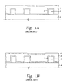
- FIG. 1A illustrates a process for depositing a gap fill layer as described in International Publication Number WO 94/01885.
- the PECVD process deposits a multi-component dielectric layer wherein a silicon dioxide (SiO 2 ) liner layer 2 is first deposited on a patterned metal layer having metal lines 3 formed on a substrate 4.
- the liner layer 2 is deposited by a plasma enhanced reaction of silane (SiH 4 ) and nitrous oxide (N 2 O) at 300°C.
- a self-planarizing low k dielectric layer 5 is then deposited on the liner layer 2 by reaction of silane and a hydroxyl compound.
- the self-planarizing layer 5 retains moisture that is removed by curing.
- the liner layer 2 is an oxidized silane film that has barrier properties when deposited in a manner which provides a dielectric constant of at least 4.5.
- the dielectric constant of the oxidized silane film can be decreased to about 4.1 by selecting process conditions less favorable for obtaining moisture barrier properties.
- Conventional liner layers, such as SiN have even higher dielectric constants, and the combination of low k dielectric layers with high k dielectric liner layers can provide little or no improvement in the overall stack dielectric constant and capacitive coupling.
- An optional SiO 2 cap layer 6 can be deposited on the self-planarizing low k dielectric layer 5 by the reaction of silane and N 2 O.
- Gap fill layers produced by reacting hydrogen peroxide with silane to form hydroxyl groups are known, but it is difficult to obtain uniform films having low dielectric constants.
- the thickness of the deposited layers on semiconductor substrates is typically controlled by providing exact amounts of reactants.
- hydrogen peroxide is typically stored as a solution in water and it is difficult to feed exact amounts of hydrogen peroxide and silane within the reaction chambers.
- TEOS tetraethoxysilane
- oxygen and/or ozone The process can include an optional source of water, such as water vapor, hydrogen peroxide, or an alcohol that forms water when oxygenated.
- the gap fill layers are deposited subsequent to plasma enhanced deposition of a conformal layer from the same components by turning off a power source used to form a plasma. The presence of water in the reactor was believed to result in a slightly improved gap fill process.
- the present invention provides a method and apparatus for uniformly depositing a silicon oxide layer having a low dielectric constant for use as a gap fill layer, a pre-metal dielectric layer, an inter-metal dielectric layer, or a shallow trench isolation dielectric layer in sub-micron devices.
- the method comprises reacting one or more silicon compounds that contain carbon (i.e., organosilicon compounds) with a hydroxyl forming compound at a substrate temperature less than about 400°C.
- the organosilicon compounds preferably contain one or more silicon-carbon bonds that remain in the deposited dielectric layers after reaction with a hydroxyl forming compound such as hydrogen peroxide or dimethyldioxirane.
- the hydroxyl forming compound may be produced prior to, or during deposition, such as by oxidation of water using ozone and UV light, by reaction of acetone and potassium monoperoxy sulfate to form dimethyldioxirane, or by oxidation or an organic compound that forms hydroxyls, such as oxidation of isopropyl alcohol with ozone or oxygen to produce acetone and hydrogen peroxide.
- the hydroxyl forming compound could be an acid such as acetic acid that provides hydrogen that reacts with siloxane compounds to form hydroxyl groups, or an acid compound that reacts with water to form hydroxyl compounds.
- the dielectric layer is produced by depositing a conformal liner layer on a patterned metal layer from process gases comprising an organosilicon compound and an oxidizing gas.
- the process is optionally plasma assisted using an RF power density from 0.05 W/cm 2 to about 1000 W/cm 2 , preferably a power density less than about 1 W/cm 2 , most preferably a power density ranging from about 0.1 to about 0.3 W/cm 2 .
- the gap fill layer is then deposited on the liner layer at a temperature less than about 300°C from process gases comprising the silicon compound and a hydroxyl forming compound, preferably less than about 40°C when using organosilicon compounds that contain silicon-carbon bonds. Deposition of uniform dielectric layers is substantially enhanced by dissociation of hydroxyl forming compounds such as water in a remote microwave or RF chamber.
- the organosilicon compounds that produce uniform, low k dielectric layers preferably include one or more silicon-hydrogen bonds such as methylsilane, CH 3 SiH 3 , dimethylsilane, (CH 3 ) 2 SiH 2 , trimethylsilane, (CH 3 ) 3 SiH, and 1,1,3,3-tetramethyldisiloxane, (CH 3 ) 2 -SiH-O-SiH-(CH 3 ) 2 .
- Gap fill layers can also be uniformily deposited from other organosilicon compounds such as tetramethylsilane, (CH 3 ) 4 Si, and tetraethylorthosilicate (TEOS).
- the silicon oxide layers are cured at low pressure and high temperature to stabilize film properties such as moisture content.
- the invention also provides a substrate processing system, having a chamber comprising a reaction zone, a substrate holder for positioning a substrate in the reaction zone, and a vacuum system, a gas distribution system connecting the reaction zone of the chamber to supplies of an organosilicon compound and a hydroxyl forming compound, an RF generator coupled to the gas distribution system for generating a plasma in the reaction zone, and a controller comprising a computer for controlling the chamber, the gas distribution system, and the RF generator.
- the controller has a memory coupled to the controller, the memory comprising a computer usable medium comprising a computer readable program code for selecting a process that deposits gap fill layers, pre-metal dielectric layers, inter-metal dielectric layers, or shallow trench isolation dielectric layers in sub-micron devices.
- the present invention provides a method and apparatus for uniformly depositing a silicon oxide layer having a low dielectric constant (k ⁇ about 4).
- the silicon oxide layer is produced by reacting an organosilicon compound, such as an organosilane or organosiloxane, with a hydroxyl forming compound such as H 2 0 2 , dimethyldioxirane, acetic acid, or water at a substrate temperature less than about 400°C.
- the silicon oxide layer can be used as a gap fill layer, a pre-metal dielectric layer, an inter-metal dielectric layer, and a shallow trench isolation dielectric layer in sub-micron devices.
- the silicon oxide layer is cured at temperatures less than about 500°C to form a carbon doped silicon oxide film.
- a gap-fill layer of the present invention is preferably deposited on a liner layer that is deposited by plasma assisted oxidation of the same or different organosilane or organosiloxane compounds. Carbon which remains in the silicon oxide layer contributes to the low dielectric constant. The remaining carbon is between about 1% and about 50% by atomic weight when the organosilicon compound contains one or more Si-C bonds.
- the silicon oxide layers are preferably produced from silicon compounds that include at least one Si-C bond, preferably at least two Si-C bonds, that is not readily removed by oxidation at processing conditions.
- Suitable organo groups also can include alkenyl and cyclohexenyl groups and functional derivatives.
- Such organosilicon compounds include:
- the liner layers are preferably prepared by oxidizing an organo silicon compound, such as listed above, with oxygen (O 2 ) or oxygen containing compounds such as nitrous oxide (N 2 O), ozone (O 3 ), or carbon dioxide (CO 2 ), preferably O 2 or N 2 O, such that the carbon content of the deposited film is from about 1 to about 50 % by atomic weight, preferably from about 5 to about 30%.
- the oxidized organo silicon layer has a dielectric constant of about 3.0 and has excellent barrier properties.
- the oxidized organo silicon layers further have high oxide content in comparison to conventional low k dielectric layers and good adhesion properties.
- Oxidizing compounds are preferably dissociated to increase reactivity prior to entering a reaction chamber.
- RF power can also be coupled to the deposition chamber to increase dissociation of the oxidizing compounds.
- the oxidizing compounds may also be dissociated in a remote microwave chamber or remote plasma chamber prior to entering the deposition chamber to reduce excessive dissociation of the silicon containing compounds.
- Deposition of the silicon oxide layer can be continuous or discontinuous. Although deposition preferably occurs in a single deposition chamber, the layer can be deposited sequentially in two or more deposition chambers. Furthermore, RF power can be cycled or pulsed to reduce heating of the substrate and promote greater porosity in the deposited film.
- the substrate is maintained at a temperature of from about -20°C to about 400°C, and preferably is maintained at a temperature of approximately -20°C to 40°C.
- an organosilicon compound as described above is oxidized during deposition by reaction with a hydroxyl forming compound such as by reaction with hydrogen peroxide (H 2 O 2 ), which can be produced in the reaction system by combining ozone (O 3 ) and water (H 2 O) 2 preferably in the presence of UV light having a wavelength of about 254 nanometers as described in US Patent No. 5,710,079 (which is incorporated by reference herein), by reaction with an oxirane compound such as dimethyldioxirane as described below, by oxidation of an organic compound as described in US Patent No. 4,303,632 (which is incorporated by reference herein), or by reaction with acetic acid as described in US Patent No.
- the gap fill layer has a carbon content that is from about 1 to about 50 % by atomic weight, most preferably about 5 to about 30%.
- the substrate is maintained at a temperature from about -20°C to about 400°C, and preferably a temperature from about -20°C to about 40°C for organosilicon compounds containing Si-C bonds.
- the gap fill layer has a dielectric constant less than about 3.5.
- the oxidized organo silicon layers further have good adhesion properties.
- the organosilicon compounds reacted with the hydroxyl forming compounds may also be used to prepare the oxidized liner layers having good barrier properties.
- the organosilicon compounds preferably include the structures: wherein each Si is bonded to one or two carbon atoms, and C is included in an organo group, preferably alkyl or alkenyl groups such as -CH 3 , -CH 2 -CH 3 , -CH 2 -, or -CH 2 -CH 2 -, or fluorinated carbon derivatives thereof.
- the carbon atoms in the fluorinated derivatives may be partially or fully fluorinated to replace hydrogen atoms.
- an organosilane or organosiloxane compound includes two or more Si atoms
- each Si is separated from another Si by -O-, -C-, or -C-C-, wherein C is included in an organo group, preferably alkyl or alkenyl groups such as -CH 2 -, -CH 2 -CH 2 -, -CH(CH 3 )-or -C(CH 3 ) 2 -, or fluorinated derivatives thereof.
- the hydrocarbon groups in the organosilicon compounds be partially or fully fluorinated to convert C-H bonds to C-F bonds.
- Many of the preferred organosilicon compounds are commercially available.
- a combination of two or more of the organosilicon compounds can be employed to provide a blend of desired properties such as dielectric constant, oxide content, hydrophobicity, film stress, and plasma etching characteristics.
- Reaction of the organosilicon compounds with hydroxyl forming compounds can occur with addition of thermal, RF, or microwave energy to dissociate the gaseous reactants, and preferably any dissociation occurs prior to entering the reactor.
- the oxidized compounds adhere to cooler surfaces such as a substrate to form a deposited film.
- the deposited films are cured within the deposition chambers to remove water at temperatures from about 100 to about 500°C, preferably above about 400°C to improve moisture barrier properties of the films.
- the deposited film has sufficient carbon content to provide barrier properties.
- the present invention further provides a substrate processing system having a chamber including a reaction zone, a substrate holder for positioning a substrate in the reaction zone, and a vacuum system.
- the processing system further comprises a gas distribution system connecting the reaction zone of the chamber to supplies of an organosilane or organosiloxane compound, an oxidizing gas, and an inert gas, and an RF generator coupled to the gas distribution system for generating a plasma in the reaction zone.
- the gas distribution system may include a supply of a hydroxyl forming compound such as dimethyldioxirane or a gas/liquid injection system for mixing gaseous reactants, such as acetone and potassium monoperoxy sulfate, or vaporizing a liquid reactant such as water, hydrogen peroxide, or an organic compound that oxidizes to form hydroxyl forming compounds and volatile byproducts.
- the processing system further comprises a controller comprising a computer for controlling the chamber and the gas distribution system, and a memory coupled to the controller, the memory comprising a computer usable medium comprising a computer readable program code for selecting the process steps of depositing a low dielectric constant film by reacting an organosilicon compound with a hydroxyl forming compound.
- Fig. 2 is a vertical, cross-section view of a parallel plate chemical vapor deposition reactor 10 having a high vacuum region 15.
- Reactor 10 contains a gas distribution manifold 11 for dispersing process gases through perforated holes in the manifold to a substrate or wafer (not shown) that rests on a substrate support plate or susceptor 12 which is raised or lowered by a lift motor 14.
- a liquid injection system (not shown), such as typically used for liquid injection of TEOS, may also be provided for injecting a liquid organosilane and/or organosiloxane compound.
- the preferred organosilicon compounds are gases.
- the reactor 10 includes heating of the process gases and substrate, such as by resistive heating coils (not shown) or external lamps (not shown).
- susceptor 12 is mounted on a support stem 13 so that susceptor 12 (and the substrate supported on the upper surface of susceptor 12) can be controllably moved between a lower loading/off-loading position and an upper processing position which is closely adjacent to manifold 11.
- susceptor 12 and the substrate When susceptor 12 and the substrate are in processing position 14, they are surrounded by an insulator 17 and process gases exhaust into a manifold 24. During processing, gases inlet to manifold 11 are uniformly distributed radially across the surface of the substrate.
- a vacuum pump 32 having a throttle valve controls the exhaust rate of gases from the chamber.
- deposition and carrier gases are input through gas lines 18 into a mixing system 19 where they are combined and then sent to manifold 11.
- the oxidizing gas may optionally be introduced through an additional chamber 28 such as a UV light chamber for decomposition of ozone, a liquid injection system as described for Figure 3 for vaporizing hydrogen peroxide or other organic compounds, a microwave applicator for dissociation of oxidizing gases such as water or N 2 O, or another energy source, such as a remote RF applicator, that assists with activation of process gases.
- the process gas supply line 18 for each of the process gases also includes (i) safety shut-off valves (not shown) that can be used to automatically or manually shut off the flow of process gas into the chamber, and (ii) mass flow controllers (also not shown) that measure the flow of gas through the gas supply lines.
- safety shut-off valves not shown
- mass flow controllers also not shown
- the deposition process performed in reactor 10 can be either a thermal process or an RF or microwave enhanced process.
- a controlled plasma is typically formed adjacent to the substrate by RF energy applied to distribution manifold 11 from RF power supply 25 (with susceptor 12 grounded).
- RF power can be provided to the susceptor 12 or RF power can be provided to different components at different frequencies.
- RF power supply 25 can supply either single or mixed frequency RF power to enhance the decomposition of reactive species introduced into the high vacuum region 15.
- a mixed frequency RF power supply typically supplies power at a high RF frequency (RF1) of 13.56 MHz to the distribution manifold 11 and at a low RF frequency (RF2) of 360 KHz to the susceptor 12.
- the silicon oxide layers of the present invention are most preferably produced using low levels of constant high frequency RF power or pulsed levels of high frequency RF power.
- Pulsed RF power preferably provides 13.56 MHz RF power at about 20W to about 500W, most preferably from 20W to about 250W, during about 10% to about 30% of the duty cycle.
- Constant RF power preferably provides 13.56 MHz RF power at about 10W to about 200W, preferably from about 20W to about 100W.
- Low power deposition preferably occurs at a temperature range from about -20°C to about 40°C. At the preferred temperature range, the deposited film is partially polymerized during deposition and polymerization is completed during subsequent curing of the film.
- an optional microwave chamber 28 described in more detail below for Fig. 3, or remote RF plasma chamber, inputs from 0 to 3000W of power to the oxidizing gas, such as water, O 2 , or N 2 0, prior to entering the deposition chamber.
- the oxidizing gas such as water, O 2 , or N 2
- separate addition of microwave or RF power to the process gas avoids excessive dissociation of the silicon compounds prior to reaction with the dissociated gas.
- a gas distribution plate having separate passages for the silicon compound and the process gas is preferred when microwave power is added to one of the process gases.
- any or all of the chamber lining, distribution manifold 11, susceptor 12, and various other reactor hardware is made out of material such as aluminum, anodized aluminum, or ceramic.
- An example of such a CVD reactor is described in U.S. Patent 5,000,113, entitled A Thermal CVD/PECVD Reactor and Use for Thermal Chemical Vapor Deposition of Silicon Dioxide and In-situ Multi-step Planarized Process, issued to Wang et al. and assigned to Applied Materials, Inc., the assignee of the present invention.
- the lift motor 14 raises and lowers susceptor 12 between a processing position and a lower, substrate-loading position.
- the motor, the gas mixing system 19, and the RF power supply 25 are controlled by a system controller 34 over control lines 36.
- the reactor includes analog assemblies, such as mass flow controllers (MFCs) and standard or pulsed RF generators, that are controlled by the system controller 34 which executes system control software stored in a memory 38, which in the preferred embodiment is a hard disk drive.
- MFCs mass flow controllers
- RF generators standard or pulsed RF generators
- the system controller 34 controls all of the activities of the CVD reactor and a preferred embodiment of the controller 34 includes a hard disk drive, a floppy disk drive, and a card rack.
- the card rack contains a single board computer (SBC), analog and digital input/output boards, interface boards and stepper motor controller boards.
- SBC single board computer
- the system controller conforms to the Versa Modular Europeans (VME) standard which defines board, card cage, and connector dimensions and types.
- VME Versa Modular Europeans
- the VME standard also defines the bus structure having a 16-bit data but and 24-bit address bus.
- the system controller 34 operates under the control of a computer program stored on the hard disk drive 38.
- the computer program dictates the timing, mixture of gases, RF power levels, susceptor position, and other parameters of a particular process.
- Fig. 3 is a simplified diagram of a remote microwave chamber 28 for dissociating process gases such as water prior to entering the reactor 10, in accordance with an embodiment of the present invention.
- Remote microwave chamber 28 includes an applicator tube 92, a plasma ignition system including an ultraviolet (UV) lamp 131 and a UV power supply 133, a microwave waveguide system that includes various lengths of straight and curved waveguide sections 115, 117, which may be connected together at joints 119, an output waveguide section 121, optimizing elements including an impedance matching system 101, which may include an optional phase detector 103 for embodiments requiring feedback for automatic impedance matching, a circulator 105 with a load 107; and a magnetron 111.
- an impedance matching system 101 which may include an optional phase detector 103 for embodiments requiring feedback for automatic impedance matching
- a circulator 105 with a load 107 and a magnetron 111.
- Magnetron 111 is a typical magnetron source capable of operating between about 0-3000 Watts for continuous wave (CW) or pulsed output of microwaves of about 2.45 Gigahertz (GHz) frequency. Of course, other magnetrons may be utilized as well.
- Circulator 105 allows only forward microwave transmission from magnetron 111 toward applicator tube 92. Load 107 absorbs any power that might be reflected back from the waveguide system toward magnetron 711. Circulator 105 connects to waveguide section 115 that is connected to phase detector 103 connected to another waveguide section 115. Phase detector 103, if utilized, is coupled via curved waveguide section 117 to another waveguide section 115 having an attached tuning or matching system 101.
- Tuning system 101 which may use stub tuners or other tuning elements, provides the microwave chamber 28 with the ability to match the load at waveguide section 121 to the characteristic impedance of the waveguides.
- Tuning system 101 may provide fixed tuning, manual tuning, or automated tuning, according to specific embodiments.
- phase detector 103 is a 3-diode array which detects the phase of microwaves transmitted for feedback to matching system 101, which intelligently and dynamically matches the load appropriately.
- the waveguide sections have rectangular cross-sections, but other types of waveguide also may be used.
- Applicator tube 92 is a circular (or other cross-section) tube made of a composite or ceramic material, preferably alumina, or other material resistant to etching by radicals.
- applicator tube 92 has a length of about 18-24 inches and a cross-sectional diameter of about 3-4 inches.
- Applicator tube 92 is disposed through a waveguide section 121, which is open at one end for transmitting microwaves and is terminated at the other end with a metal wall. Microwaves are transmitted through the open end of waveguide section 121 to gases inside applicator tube 92, which is transparent to microwaves.
- other materials such as sapphire also may be used for the interior of applicator tube 92.
- applicator tube 92 may have a metal exterior and an interior made of a composite or ceramic material wherein microwaves in waveguide section 121 enter a window through the exterior of applicator tube 92 to the exposed interior of tube 92 to energize the gases.
- Fig. 4 shows an alternative method for providing a hydroxyl compound to the reactor 10.
- the optional chamber 28 in Fig. 2 is a liquid injection system 42 having a flow controller 44 that precisely meters flow of water, hydrogen peroxide, or other liquid reactants, such as 2-ethyl-anthrahydroquinone, benzhydrol, or isopropyl alcohol, prior to volatilization and mixing with other gases, such as oxygen and/or ozone, in the mixing chamber 19.
- the uniform flow of liquid from the injection system 42 is obtained by introducing a non-reactive gas, typically helium, into the system 42 and displacing a known volume of liquid.
- the liquid is optionally vaporized in an energy chamber 44 such as a microwave chamber or a UV chamber prior to entering the mixing chamber 19.
- the flow of oxidizing gas or hydroxyl forming gas is measured with a flow meter 40 to provide precise control of the flow of reactants.
- the reactor pump 32 draws the combined gases from the mixing chamber 19.
- the combined gases could also be passed through a microwave chamber 28 or other chamber to dissociate the gas as described for Fig. 3.
- the process of the invention can be implemented using a computer program product 410 that runs on, for example, the system controller 34.
- the computer program code can be written in any conventional computer readable programming language such as for example 68000 assembly language, C, C++, or Pascal. Suitable program code is entered into a single file, or multiple files, using a conventional text editor, and stored or embodied in a computer usable medium, such as a memory system of the computer. If the entered code text is in a high level language, the code is compiled, and the resultant compiler code is then linked with an object code of precompiled windows library routines. To execute the linked compiled object code, the system user invokes the object code, causing the computer system to load the code in memory, from which the CPU reads and executes the code to perform the tasks identified in the program.
- Fig. 5 shows an illustrative block diagram of the hierarchical control structure of the computer program 410.
- a user enters a process set number and process chamber number into a process selector subroutine 420.
- the process sets are predetermined sets of process parameters necessary to carry out specified processes, and are identified by predefined set numbers.
- the process selector subroutine 420 the (i) selects a desired process chamber on a cluster tool such as an Centura(r) platform (available from Applied Materials, Inc.), and (ii) selects a desired set of process parameters needed to operate the process chamber for performing the desired process.
- the process parameters for performing a specific process relate to process conditions such as, for example, process gas composition and flow rates, temperature, pressure, plasma conditions such as RF bias power levels and magnetic field power levels, cooling gas pressure, and chamber wall temperature and are provided to the user in the form of a recipe.
- process conditions such as, for example, process gas composition and flow rates, temperature, pressure, plasma conditions such as RF bias power levels and magnetic field power levels, cooling gas pressure, and chamber wall temperature and are provided to the user in the form of a recipe.
- the parameters specified by the recipe are entered utilizing the light pen/CRT monitor interface.
- the signals for monitoring the process are provided by the analog input and digital input boards of system controller and the signals for controlling the process are output on the analog output and digital output boards of the system controller 34.
- a process sequencer subroutine 430 comprises program code for accepting the identified process chamber and set of process parameters from the process selector subroutine 420, and for controlling operation of the various process chambers. Multiple users can enter process set numbers and process chamber numbers, or a user can enter multiple process chamber numbers, so the sequencer subroutine 430 operates to schedule the selected processes in the desired sequence.
- the sequencer subroutine 430 includes computer readable program code to perform the steps of (i) monitoring the operation of the process chambers to determine if the chambers are being used, (ii) determining what processes are being carried out in the chambers being used, and (iii) executing the desired process based on availability of a process chamber and type of process to be carried out.
- sequencer subroutine 430 can be designed to take into consideration the present condition of the process chamber being used in comparison with the desired process conditions for a selected process, or the "age" of each particular user entered request, or any other relevant factor a system programmer desires to include for determining the scheduling priorities.
- the sequencer subroutine 430 determines which process chamber and process set combination is going to be executed next, the sequencer subroutine 430 causes execution of the process set by passing the particular process set parameters to a chamber manager subroutine 440 which controls multiple processing tasks in a reactor 10 according to the process set determined by the sequencer subroutine 430.
- the chamber manager subroutine 440 comprises program code for controlling CVD process operations in the process chamber 10.
- the chamber manager subroutine 440 also controls execution of various chamber component subroutines which control operation of the chamber component necessary to carry out the selected process set.
- chamber component subroutines are susceptor control subroutine 450, process gas control subroutine 460, pressure control subroutine 470, heater control subroutine 480, and plasma control subroutine 490.
- process gas control subroutine 460 processes gas control subroutine 460
- pressure control subroutine 470 pressure control subroutine 470
- heater control subroutine 480 heater control subroutine 480
- plasma control subroutine 490 plasma control subroutine
- the chamber manager subroutine 440 selectively schedules or calls the process component subroutines in accordance with the particular process set being executed.
- the chamber manager subroutine 440 schedules the process component subroutines similarly to how the sequencer subroutine 430 schedules which reactor 10 and process set is to be executed next.
- the chamber manager subroutine 440 includes steps of monitoring the various chamber components, determining which components needs to be operated based on the process parameters for the process set to be executed, and causing execution of a chamber component subroutine responsive to the monitoring and determining steps.
- the susceptor control positioning subroutine 450 comprises program code for controlling chamber components that are used to load the substrate onto the susceptor 12, and optionally to lift the substrate to a desired height in the reactor 10 to control the spacing between the substrate and the gas distribution manifold 11.
- the susceptor 12 is lowered to receive the substrate, and thereafter, the susceptor 12 is raised to the desired height in the chamber, to maintain the substrate at a first distance or spacing from the gas distribution manifold 11 during the CVD process.
- the susceptor control subroutine 450 controls movement of the susceptor 12 in response to process set parameters that are transferred from the chamber manager subroutine 440.
- the process gas control subroutine 460 has program code for controlling process gas composition and flow rates.
- the process gas control subroutine 460 controls the open/close position of the safety shut-off valves, and also ramps up/down the mass flow controllers to obtain the desired gas flow rate.
- the process gas control subroutine 460 is invoked by the chamber manager subroutine 440, as are all chamber components subroutines, and receives from the chamber manager subroutine process parameters related to the desired gas flow rates.
- the process gas control subroutine 460 operates by opening the gas supply lines, and repeatedly (i) reading the necessary mass flow controllers, (ii) comparing the readings to the desired flow rates received from the chamber manager subroutine 440, and (iii) adjusting the flow rates of the gas supply lines as necessary. Furthermore, the process gas control subroutine 460 includes steps for monitoring the gas flow rates for unsafe rates, and activating the safety shut-off valves when an unsafe condition is detected.
- a non-reactive gas such as helium, argon, or nitrogen is flowed into the reactor 10 to stabilize the pressure in the chamber before reactive process gases are introduced into the chamber.
- the process gas control subroutine 460 is programmed to include steps for flowing the inert gas into the reactor 10 for an amount of time necessary to stabilize the pressure in the chamber, and then the steps described above would be carried out.
- a process gas is to be vaporized from a liquid precursor, for example isopropyl alcohol
- the process gas control subroutine 460 would be written to include steps for bubbling a delivery gas such as ozone through the liquid precursor in a bubbler 42.
- the process gas control subroutine 460 regulates the flow of the delivery gas, the pressure in the bubbler, and the bubbler temperature in order to obtain the desired process gas flow rates.
- the desired process gas flow rates are transferred to the process gas control subroutine 460 as process parameters.
- the process gas control subroutine 460 includes steps for obtaining the necessary delivery gas flow rate, bubbler pressure, and bubbler temperature for the desired process gas flow rate by accessing a stored table containing the necessary values for a given process gas flow rate. Once the necessary values are obtained, the delivery gas flow rate, bubbler pressure and bubbler temperature are monitored, compared to the necessary values and adjusted accordingly.
- the pressure control subroutine 470 comprises program code for controlling the pressure in the reactor 10 by regulating the size of the opening of the throttle valve in the exhaust pump 32.
- the size of the opening of the throttle valve is set to control the chamber pressure to the desired level in relation to the total process gas flow, size of the process chamber, and pumping set point pressure for the exhaust pump 32.
- the pressure control subroutine 470 is invoked, the desired, or target pressure level is received as a parameter from the chamber manager subroutine 440.
- the pressure control subroutine 470 operates to measure the pressure in the reactor 10 by reading one or more conventional pressure manometers connected to the chamber, compare the measure value(s) to the target pressure, obtain PID (proportional, integral, and differential) values from a stored pressure table corresponding to the target pressure, and adjust the throttle valve according to the PID values obtained from the pressure table.
- the pressure control subroutine 470 can be written to open or close the throttle valve to a particular opening size to regulate the reactor 10 to the desired pressure.
- the heater control subroutine 480 comprises program code for controlling the temperature of the heat modules or radiated heat that is used to heat the susceptor 12.
- the heater control subroutine 480 is also invoked by the chamber manager subroutine 440 and receives a target, or set point, temperature parameter.
- the heater control subroutine 480 measures the temperature by measuring voltage output of a thermocouple located in a susceptor 12, compares the measured temperature to the set point temperature, and increases or decreases current applied to the heat module to obtain the set point temperature.
- the temperature is obtained from the measured voltage by looking up the corresponding temperature in a stored conversion table, or by calculating the temperature using a fourth order polynomial.
- the heater control subroutine 480 gradually controls a ramp up/down of current applied to the heat module. The gradual ramp up/down increases the life and reliability of the heat module. Additionally, a built-in-fail-safe mode can be included to detect process safety compliance, and can shut down operation of the heat module if the reactor 10 is not properly set
- the plasma control subroutine 490 comprises program code for setting the RF bias voltage power level applied to the process electrodes in the reactor 10, and optionally, to set the level of the magnetic field generated in the reactor. Similar to the previously described chamber component subroutines, the plasma control subroutine 490 is invoked by the chamber manager subroutine 440.
- CVD system description is mainly for illustrative purposes, and other plasma CVD equipment such as electrode cyclotron resonance (ECR) plasma CVD devices, induction-coupled RF high density plasma CVD devices, or the like may be employed. Additionally, variations of the above described system such as variations in susceptor design, heater design, location of RF power connections and others are possible. For example, the substrate could be supported and heated by a resistively heated susceptor.
- ECR electrode cyclotron resonance
- the oxidized organosilane or organosiloxane layer of the present invention can be used to replace silicon oxide layers in most applications.
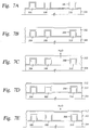
- An embodiment that demonstrates the versatility of the present invention is a three-layer gap fill process as shown in Fig. 6 using the reactor of Figure 2. Referring to Fig. 6, a substrate is positioned 200 in the reactor 10 and an oxidized organosilane layer having a low dielectric constant is deposited 205 by a PECVD process from a plasma comprising an organosilane compound and/or an organosiloxane compound, and an oxidizing gas such as O 2 or N 2 O.
- the deposition step 205 can include a capacitively coupled plasma or both an inductively and a capacitively coupled plasma in the chamber 15 according to methods known in the art.
- An inert gas such as helium is commonly used in the PECVD process to assist in plasma generation.
- a gap fill layer is then deposited 210 on the liner layer in accordance with the present invention, preferably by reacting an organosilane or organosiloxane compound used to produce the liner layer with a hydroxyl forming compound.
- the gap fill layer is preferably self-planarizing, and preferably is hydrophobic after curing to remove water.
- a cap layer is then deposited 215 on the gap fill layer, preferably using the same process for depositing the liner layer.
- the substrate is then removed 220 from the reactor 10.
- the three-layer gap fill process provides a PECVD liner layer 300 of the oxidized organosilane or organosiloxane polymer.
- the liner layer 300 acts as an isolation layer between a subsequent gap fill layer 302 and the underlying substrate surface 304 and metal lines 306, 308, 310 formed on the substrate surface.
- the gap fill layer 302 is capped by a PECVD capping layer 312 of the oxidized organosilane or organosiloxane polymer.
- This process is implemented and controlled using a computer program stored in the memory 38 of a computer controller 34 for a CVD reactor 10. Referring to Fig.
- the PECVD liner layer 300 is deposited in the reactor 10 by introducing an oxidizing gas such as N2O, an organosilane or organosiloxane compound such as methylsilane (CH 3 SiH 3 ), trimethylsilane ((CH 3 ) 3 SiH), or the like, and a carrier gas such as helium.
- the substrate is maintained at a temperature of from about -20°C to about 400°C, and preferably is maintained at a temperature of approximately -20°C to 40°C throughout the deposition of the PECVD liner layer.
- the PECVD liner layer 300 is deposited with a process gas that includes a mixture of the organosilane and/or organosiloxane compound at a flow rate of about 5 sccm to about 500 sccm and the oxidizing gas at a flow rate of about 5 sccm to about 2000 sccm.
- the process gases are carried by an inert gas such He, Ar, or a relatively inert gas such as nitrogen, which are typically not incorporated into the film, at a flow rate of from about 200 sccm to about 20,000 sccm.
- the process gases react at a pressure from about 0.2 to about 20 Torr, preferably less than about 10 Torr, to form a conformal silicon oxide layer on the substrate surface 304 and metal lines 306, 308, 310.
- the reaction is plasma enhanced with a power density ranging from about 0.05 W/cm2 to about 1000 W/cm 2 , preferably a power density less than about 1 W/cm 2 , most preferably a power density ranging from about 0.1 to about 0.3 W/cm 2 .
- the high frequency RF source of approximately 13.56 MHz is preferably connected to a gas distribution system and driven at about 10 to about 500 W while a low frequency RF source of about 350 KHz to 1 MHz is optionally connected to a susceptor and driven at about 0 to about 100W.
- the high frequency RF source is driven at about 20W to about 250 W of pulsed RF power
- the low frequency RF source is driven at about 0 to about 50W of pulsed RF power at a duty cycle from about 10% to about 30%.
- the pulsed RF power is preferably cycled in short intervals, most preferably having a frequency less than about 200 Hz.
- the power level preferably ranges from about 20W to about 100W.
- the oxidized organosilane or organosiloxane layer is then cured at a pressure less than about 10 Torr a temperature from about 300°C to about 500°C.
- curing could be conducted after deposition of additional dielectric layers.
- the above process conditions result in the deposition of a PECVD liner layer 300 at about 2000 ⁇ per minute with improved barrier characteristics for the subsequent deposition of the gap fill layer 302 shown in Fig. 7B.
- the liner layer obtained from methylsilane has sufficient C-H bonds to be hydrophobic, and is an excellent moisture barrier.
- Deposition of a hydrophobic liner layer has a surprising and unexpected result of converting subsequent hydrophilic gap filling layers to hydrophobic layers having good moisture barrier properties.
- the process gases for the gap fill layer 302 may include any organosilicon compound, but preferably include the same organosilicon compounds used for the liner layer.
- the process gases further include a hydroxyl forming compound such as hydrogen peroxide, dimethyldioxirane, water, and isopropyl alcohol.
- Hydrogen peroxide is preferably about 50 wt% of hydrogen peroxide (H 2 O 2 ) which is vaporized and mixed with an inert carrier gas, such as helium.
- the hydroxyl forming compound can alternatively be formed in the reaction system as previously described.
- the process gas flows range from 0-8000 sccm for He, 10-1200 sccm for the organosilicon compound, such as (CH 3 ) x SiH 4-x , and 20-3000 sccm for the hydroxyl forming compound, such as H 2 O 2 or dimethyldioxirane.
- the preferred gas flows range from 500-4000 sccm for He, 100-500 sccm for (CH 3 ) x SiH 4-x , and 100-1000 sccm for hydroxyl forming compounds. These flow rates are for a chamber having a volume of about 5.5 to 6.5 liters.
- the flows range from 2,000-6,000 sccm for oxidizing gases, such as oxygen, containing about 6-20 wt% ozone, and from 500-2000 mg/min for water or other hydroxyl sources.
- reactor 10 is maintained at a pressure of about 0.2 to about 5 torr and maintains a substrate temperature less than about 40°C during deposition of the gap fill layer 302.
- the temperature of the gas distribution system within the reactor preferably is maintained at a temperature from about 70°C to about 130°C.
- the gap fill layer 302 may be partially cured as shown in Fig. 7C to remove solvents such as water prior to deposition of a cap layer 312 as shown in Fig. 7D. Curing is preferably done in a thermal annealing chamber or in the reactor 10 by maintaining a vacuum under 10 Torr in an inert gas atmosphere.
- Gap fill layers produced from methylsilane are typically hydrophilic and have poor moisture barrier properties.
- a gap fill layer produced from methylsilane is hydrophobic and has good moisture barrier properties.
- the reactor 10 optionally resumes deposition of the oxidized organosilane or organosiloxane layer of the present invention for deposition of a capping layer 312.
- the deposited layers are cured in a furnace or another chamber at a temperature from about 300°C to about 500°C to drive off remaining solvent or water.
- processing conditions will vary according to the desired characteristics of the deposited films. The invention is further described by the following examples.
- the following examples illustrate reaction of an organosilicon compound and hydroxyl forming compounds to deposit dielectric layers having low dielectric constants.
- the examples refer to a chemical vapor deposition chamber, and in particular, a "CENTURA DxZ" system which includes a solid-state RF matching unit with a two-piece quartz process kit, both fabricated and sold by Applied Materials, Inc., Santa Clara, California.
- An oxidized trimethylsilane film is deposited at a chamber pressure of 3.0 Torr and a substrate temperature of 0°C from reactive gases which are flowed into the reactor as follows:
- the substrate is positioned from 200-1000 mils from the gas distribution showerhead, preferably 600 mils, and deposition occurs to a depth from about 1000 ⁇ to 2 (m.
- the film is then cured at a temperature of 400°C for about 30 to about 120 minutes.
- the oxidized trimethylsilane material is estimated to have a dielectric constant less than about 3.0.
- An oxidized trimethylsilane layer is deposited at a chamber pressure of 3.0 Torr and a substrate temperature of 25°C from reactive gases which are flowed into the reactor as follows:
- a dimethylsilane layer is deposited at a chamber pressure of 3.0 Torr and a substrate temperature of 25°C from reactive gases which are flowed into the reactor as follows:
Landscapes
- Chemical & Material Sciences (AREA)
- Inorganic Chemistry (AREA)
- General Chemical & Material Sciences (AREA)
- Chemical Kinetics & Catalysis (AREA)
- Engineering & Computer Science (AREA)
- Materials Engineering (AREA)
- Mechanical Engineering (AREA)
- Metallurgy (AREA)
- Organic Chemistry (AREA)
- Formation Of Insulating Films (AREA)
- Chemical Vapour Deposition (AREA)
- Internal Circuitry In Semiconductor Integrated Circuit Devices (AREA)
Applications Claiming Priority (2)
| Application Number | Priority Date | Filing Date | Title |
|---|---|---|---|
| US338470 | 1999-06-22 | ||
| US09/338,470 US6413583B1 (en) | 1998-02-11 | 1999-06-22 | Formation of a liquid-like silica layer by reaction of an organosilicon compound and a hydroxyl forming compound |
Publications (1)
| Publication Number | Publication Date |
|---|---|
| EP1063692A1 true EP1063692A1 (fr) | 2000-12-27 |
Family
ID=23324944
Family Applications (1)
| Application Number | Title | Priority Date | Filing Date |
|---|---|---|---|
| EP00112820A Withdrawn EP1063692A1 (fr) | 1999-06-22 | 2000-06-16 | Procédé de dépot d'un film à faible constante diélectrique |
Country Status (5)
| Country | Link |
|---|---|
| US (1) | US6413583B1 (fr) |
| EP (1) | EP1063692A1 (fr) |
| JP (2) | JP2001148382A (fr) |
| KR (1) | KR100787657B1 (fr) |
| TW (1) | TW457630B (fr) |
Cited By (19)
| Publication number | Priority date | Publication date | Assignee | Title |
|---|---|---|---|---|
| EP1148150A2 (fr) | 2000-04-21 | 2001-10-24 | Applied Materials, Inc. | Procédé et appareillage pour le traitement des substrats de sémiconducteur par des radicaux hydroxylés |
| US6340435B1 (en) | 1998-02-11 | 2002-01-22 | Applied Materials, Inc. | Integrated low K dielectrics and etch stops |
| US6511923B1 (en) * | 2000-05-19 | 2003-01-28 | Applied Materials, Inc. | Deposition of stable dielectric films |
| WO2002091451A3 (fr) * | 2001-05-07 | 2003-07-03 | Applied Materials Inc | Procedes de remplissage d'espaces et couches formees selon lesdits procedes |
| EP1302981A3 (fr) * | 2001-10-10 | 2004-06-02 | Fujitsu Limited | Procédé pour la fabrication d'un dispositif semiconducteur avec une couche de carbure de silicium |
| DE102004020328A1 (de) * | 2004-04-26 | 2005-11-03 | Infineon Technologies Ag | Verfahren zur Abscheidung einer mit Kohlenstoff dotierten siliziumhaltigen dielektrischen Schicht |
| EP1482550A3 (fr) * | 2003-05-30 | 2009-07-29 | National Institute of Advanced Industrial Science and Technology | Couche isolante avec constante dielectrique basse et sa fabrication |
| US8809161B2 (en) | 2004-03-25 | 2014-08-19 | Novellus Systems, Inc. | Flowable film dielectric gap fill process |
| US8846536B2 (en) | 2012-03-05 | 2014-09-30 | Novellus Systems, Inc. | Flowable oxide film with tunable wet etch rate |
| US9064684B1 (en) | 2009-09-24 | 2015-06-23 | Novellus Systems, Inc. | Flowable oxide deposition using rapid delivery of process gases |
| US9245739B2 (en) | 2006-11-01 | 2016-01-26 | Lam Research Corporation | Low-K oxide deposition by hydrolysis and condensation |
| US9257302B1 (en) | 2004-03-25 | 2016-02-09 | Novellus Systems, Inc. | CVD flowable gap fill |
| US9719169B2 (en) | 2010-12-20 | 2017-08-01 | Novellus Systems, Inc. | System and apparatus for flowable deposition in semiconductor fabrication |
| US9847222B2 (en) | 2013-10-25 | 2017-12-19 | Lam Research Corporation | Treatment for flowable dielectric deposition on substrate surfaces |
| US9916977B2 (en) | 2015-11-16 | 2018-03-13 | Lam Research Corporation | Low k dielectric deposition via UV driven photopolymerization |
| US10049921B2 (en) | 2014-08-20 | 2018-08-14 | Lam Research Corporation | Method for selectively sealing ultra low-k porous dielectric layer using flowable dielectric film formed from vapor phase dielectric precursor |
| US10388546B2 (en) | 2015-11-16 | 2019-08-20 | Lam Research Corporation | Apparatus for UV flowable dielectric |
| US12060639B2 (en) | 2019-04-19 | 2024-08-13 | Lam Research Corporation | Rapid flush purging during atomic layer deposition |
| TWI883840B (zh) * | 2018-09-17 | 2025-05-11 | 美商應用材料股份有限公司 | 沉積介電材料之方法 |
Families Citing this family (518)
| Publication number | Priority date | Publication date | Assignee | Title |
|---|---|---|---|---|
| US6054379A (en) | 1998-02-11 | 2000-04-25 | Applied Materials, Inc. | Method of depositing a low k dielectric with organo silane |
| US6660656B2 (en) | 1998-02-11 | 2003-12-09 | Applied Materials Inc. | Plasma processes for depositing low dielectric constant films |
| US6303523B2 (en) | 1998-02-11 | 2001-10-16 | Applied Materials, Inc. | Plasma processes for depositing low dielectric constant films |
| US6593247B1 (en) * | 1998-02-11 | 2003-07-15 | Applied Materials, Inc. | Method of depositing low k films using an oxidizing plasma |
| US6287990B1 (en) | 1998-02-11 | 2001-09-11 | Applied Materials, Inc. | CVD plasma assisted low dielectric constant films |
| US6800571B2 (en) * | 1998-09-29 | 2004-10-05 | Applied Materials Inc. | CVD plasma assisted low dielectric constant films |
| US6974766B1 (en) | 1998-10-01 | 2005-12-13 | Applied Materials, Inc. | In situ deposition of a low κ dielectric layer, barrier layer, etch stop, and anti-reflective coating for damascene application |
| US6251770B1 (en) * | 1999-06-30 | 2001-06-26 | Lam Research Corp. | Dual-damascene dielectric structures and methods for making the same |
| US6689284B1 (en) * | 1999-09-29 | 2004-02-10 | Kabushiki Kaisha Toshiba | Surface treating method |
| US6794295B1 (en) * | 2000-05-26 | 2004-09-21 | Taiwan Semiconductor Manufacturing Company, Ltd. | Method to improve stability and reliability of CVD low K dielectric |
| US6541401B1 (en) * | 2000-07-31 | 2003-04-01 | Applied Materials, Inc. | Wafer pretreatment to decrease rate of silicon dioxide deposition on silicon nitride compared to silicon substrate |
| US6762132B1 (en) * | 2000-08-31 | 2004-07-13 | Micron Technology, Inc. | Compositions for dissolution of low-K dielectric films, and methods of use |
| US6531398B1 (en) | 2000-10-30 | 2003-03-11 | Applied Materials, Inc. | Method of depositing organosillicate layers |
| WO2002075801A2 (fr) * | 2000-11-07 | 2002-09-26 | Tokyo Electron Limited | Procede de fabrication d'oxydes a faibles frequences de defauts |
| US6649219B2 (en) * | 2001-02-23 | 2003-11-18 | Lsi Logic Corporation | Process for forming a low dielectric constant fluorine and carbon-containing silicon oxide dielectric material characterized by improved resistance to oxidation |
| US6472333B2 (en) | 2001-03-28 | 2002-10-29 | Applied Materials, Inc. | Silicon carbide cap layers for low dielectric constant silicon oxide layers |
| US6486082B1 (en) * | 2001-06-18 | 2002-11-26 | Applied Materials, Inc. | CVD plasma assisted lower dielectric constant sicoh film |
| US6559033B1 (en) * | 2001-06-27 | 2003-05-06 | Lsi Logic Corporation | Processing for forming integrated circuit structure with low dielectric constant material between closely spaced apart metal lines |
| CN1305119C (zh) * | 2001-08-30 | 2007-03-14 | 东京毅力科创株式会社 | 成膜方法和成膜装置 |
| US6759327B2 (en) * | 2001-10-09 | 2004-07-06 | Applied Materials Inc. | Method of depositing low k barrier layers |
| US6838393B2 (en) * | 2001-12-14 | 2005-01-04 | Applied Materials, Inc. | Method for producing semiconductor including forming a layer containing at least silicon carbide and forming a second layer containing at least silicon oxygen carbide |
| US7091137B2 (en) * | 2001-12-14 | 2006-08-15 | Applied Materials | Bi-layer approach for a hermetic low dielectric constant layer for barrier applications |
| US6890850B2 (en) | 2001-12-14 | 2005-05-10 | Applied Materials, Inc. | Method of depositing dielectric materials in damascene applications |
| US6699784B2 (en) | 2001-12-14 | 2004-03-02 | Applied Materials Inc. | Method for depositing a low k dielectric film (K>3.5) for hard mask application |
| US7390755B1 (en) | 2002-03-26 | 2008-06-24 | Novellus Systems, Inc. | Methods for post etch cleans |
| US6936309B2 (en) | 2002-04-02 | 2005-08-30 | Applied Materials, Inc. | Hardness improvement of silicon carboxy films |
| US20030194496A1 (en) * | 2002-04-11 | 2003-10-16 | Applied Materials, Inc. | Methods for depositing dielectric material |
| US20030211244A1 (en) * | 2002-04-11 | 2003-11-13 | Applied Materials, Inc. | Reacting an organosilicon compound with an oxidizing gas to form an ultra low k dielectric |
| US20030194495A1 (en) * | 2002-04-11 | 2003-10-16 | Applied Materials, Inc. | Crosslink cyclo-siloxane compound with linear bridging group to form ultra low k dielectric |
| US6815373B2 (en) * | 2002-04-16 | 2004-11-09 | Applied Materials Inc. | Use of cyclic siloxanes for hardness improvement of low k dielectric films |
| US20030206337A1 (en) * | 2002-05-06 | 2003-11-06 | Eastman Kodak Company | Exposure apparatus for irradiating a sensitized substrate |
| US6927178B2 (en) * | 2002-07-11 | 2005-08-09 | Applied Materials, Inc. | Nitrogen-free dielectric anti-reflective coating and hardmask |
| US7105460B2 (en) * | 2002-07-11 | 2006-09-12 | Applied Materials | Nitrogen-free dielectric anti-reflective coating and hardmask |
| GB2406583B (en) * | 2002-08-08 | 2005-12-21 | Trikon Technologies Ltd | Improvements to showerheads |
| US7192486B2 (en) * | 2002-08-15 | 2007-03-20 | Applied Materials, Inc. | Clog-resistant gas delivery system |
| JP2004109888A (ja) * | 2002-09-20 | 2004-04-08 | Yasuo Kokubu | 光導波路及びその製造方法 |
| US7749563B2 (en) * | 2002-10-07 | 2010-07-06 | Applied Materials, Inc. | Two-layer film for next generation damascene barrier application with good oxidation resistance |
| US7270713B2 (en) * | 2003-01-07 | 2007-09-18 | Applied Materials, Inc. | Tunable gas distribution plate assembly |
| US6790788B2 (en) * | 2003-01-13 | 2004-09-14 | Applied Materials Inc. | Method of improving stability in low k barrier layers |
| US6897163B2 (en) * | 2003-01-31 | 2005-05-24 | Applied Materials, Inc. | Method for depositing a low dielectric constant film |
| US20040163590A1 (en) * | 2003-02-24 | 2004-08-26 | Applied Materials, Inc. | In-situ health check of liquid injection vaporizer |
| US7011890B2 (en) * | 2003-03-03 | 2006-03-14 | Applied Materials Inc. | Modulated/composited CVD low-k films with improved mechanical and electrical properties for nanoelectronic devices |
| US7208389B1 (en) * | 2003-03-31 | 2007-04-24 | Novellus Systems, Inc. | Method of porogen removal from porous low-k films using UV radiation |
| US6942753B2 (en) | 2003-04-16 | 2005-09-13 | Applied Materials, Inc. | Gas distribution plate assembly for large area plasma enhanced chemical vapor deposition |
| US20040211357A1 (en) * | 2003-04-24 | 2004-10-28 | Gadgil Pradad N. | Method of manufacturing a gap-filled structure of a semiconductor device |
| US20070231485A1 (en) * | 2003-09-05 | 2007-10-04 | Moffat William A | Silane process chamber with double door seal |
| RU2241068C1 (ru) * | 2003-10-09 | 2004-11-27 | Федеральное государственное унитарное предприятие "Московское машиностроительное производственное предприятие "Салют" | Способ получения композиционного материала |
| US7390537B1 (en) | 2003-11-20 | 2008-06-24 | Novellus Systems, Inc. | Methods for producing low-k CDO films with low residual stress |
| US6909934B1 (en) * | 2004-01-05 | 2005-06-21 | Taiwan Semiconductor Manufacturing Company, Ltd. | Efficient method of dynamic formulation of chamber selections for multiple chamber tools |
| US7381662B1 (en) | 2004-03-11 | 2008-06-03 | Novellus Systems, Inc. | Methods for improving the cracking resistance of low-k dielectric materials |
| US7341761B1 (en) * | 2004-03-11 | 2008-03-11 | Novellus Systems, Inc. | Methods for producing low-k CDO films |
| US7030041B2 (en) | 2004-03-15 | 2006-04-18 | Applied Materials Inc. | Adhesion improvement for low k dielectrics |
| US7582555B1 (en) | 2005-12-29 | 2009-09-01 | Novellus Systems, Inc. | CVD flowable gap fill |
| US7781351B1 (en) | 2004-04-07 | 2010-08-24 | Novellus Systems, Inc. | Methods for producing low-k carbon doped oxide films with low residual stress |
| US7229911B2 (en) | 2004-04-19 | 2007-06-12 | Applied Materials, Inc. | Adhesion improvement for low k dielectrics to conductive materials |
| US7622400B1 (en) | 2004-05-18 | 2009-11-24 | Novellus Systems, Inc. | Method for improving mechanical properties of low dielectric constant materials |
| US20050277302A1 (en) * | 2004-05-28 | 2005-12-15 | Nguyen Son V | Advanced low dielectric constant barrier layers |
| US7229041B2 (en) * | 2004-06-30 | 2007-06-12 | Ohio Central Steel Company | Lifting lid crusher |
| US7288205B2 (en) | 2004-07-09 | 2007-10-30 | Applied Materials, Inc. | Hermetic low dielectric constant layer for barrier applications |
| US7288484B1 (en) | 2004-07-13 | 2007-10-30 | Novellus Systems, Inc. | Photoresist strip method for low-k dielectrics |
| US20060021703A1 (en) * | 2004-07-29 | 2006-02-02 | Applied Materials, Inc. | Dual gas faceplate for a showerhead in a semiconductor wafer processing system |
| US7326444B1 (en) | 2004-09-14 | 2008-02-05 | Novellus Systems, Inc. | Methods for improving integration performance of low stress CDO films |
| US7695765B1 (en) | 2004-11-12 | 2010-04-13 | Novellus Systems, Inc. | Methods for producing low-stress carbon-doped oxide films with improved integration properties |
| US8193096B2 (en) | 2004-12-13 | 2012-06-05 | Novellus Systems, Inc. | High dose implantation strip (HDIS) in H2 base chemistry |
| US7202176B1 (en) * | 2004-12-13 | 2007-04-10 | Novellus Systems, Inc. | Enhanced stripping of low-k films using downstream gas mixing |
| US7166531B1 (en) | 2005-01-31 | 2007-01-23 | Novellus Systems, Inc. | VLSI fabrication processes for introducing pores into dielectric materials |
| US8129281B1 (en) | 2005-05-12 | 2012-03-06 | Novellus Systems, Inc. | Plasma based photoresist removal system for cleaning post ash residue |
| US7524750B2 (en) * | 2006-04-17 | 2009-04-28 | Applied Materials, Inc. | Integrated process modulation (IPM) a novel solution for gapfill with HDP-CVD |
| WO2007140424A2 (fr) * | 2006-05-30 | 2007-12-06 | Applied Materials, Inc. | DÉpÔt chimique en phase vapeur de dioxyde de silicium À Écoulement de haute qualitÉ À partir d'un prÉcurseur contenant du silicium et d'oxygÈne atomique |
| EP2036120A4 (fr) * | 2006-05-30 | 2012-02-08 | Applied Materials Inc | Nouveau procede combinant depot et durcissement par plasma permettant d'ameliorer la qualite d'un film de dioxyde de silicium |
| US7498273B2 (en) * | 2006-05-30 | 2009-03-03 | Applied Materials, Inc. | Formation of high quality dielectric films of silicon dioxide for STI: usage of different siloxane-based precursors for harp II—remote plasma enhanced deposition processes |
| US7790634B2 (en) * | 2006-05-30 | 2010-09-07 | Applied Materials, Inc | Method for depositing and curing low-k films for gapfill and conformal film applications |
| US8232176B2 (en) * | 2006-06-22 | 2012-07-31 | Applied Materials, Inc. | Dielectric deposition and etch back processes for bottom up gapfill |
| WO2008020592A1 (fr) * | 2006-08-15 | 2008-02-21 | Jsr Corporation | Matériau filmogène, film isolant contenant du silicium et procédé de formation de celui-ci |
| US7740768B1 (en) | 2006-10-12 | 2010-06-22 | Novellus Systems, Inc. | Simultaneous front side ash and backside clean |
| US7888273B1 (en) | 2006-11-01 | 2011-02-15 | Novellus Systems, Inc. | Density gradient-free gap fill |
| US20080124946A1 (en) * | 2006-11-28 | 2008-05-29 | Air Products And Chemicals, Inc. | Organosilane compounds for modifying dielectrical properties of silicon oxide and silicon nitride films |
| US7906174B1 (en) | 2006-12-07 | 2011-03-15 | Novellus Systems, Inc. | PECVD methods for producing ultra low-k dielectric films using UV treatment |
| KR20090119903A (ko) * | 2007-02-14 | 2009-11-20 | 제이에스알 가부시끼가이샤 | 규소 함유 막 형성용 재료, 및 규소 함유 절연막 및 그의 형성 방법 |
| US8435895B2 (en) | 2007-04-04 | 2013-05-07 | Novellus Systems, Inc. | Methods for stripping photoresist and/or cleaning metal regions |
| WO2009008424A1 (fr) * | 2007-07-10 | 2009-01-15 | Jsr Corporation | Procédé de production d'un composé de silicium |
| US8357435B2 (en) | 2008-05-09 | 2013-01-22 | Applied Materials, Inc. | Flowable dielectric equipment and processes |
| US8591661B2 (en) | 2009-12-11 | 2013-11-26 | Novellus Systems, Inc. | Low damage photoresist strip method for low-K dielectrics |
| US10378106B2 (en) | 2008-11-14 | 2019-08-13 | Asm Ip Holding B.V. | Method of forming insulation film by modified PEALD |
| US8557712B1 (en) * | 2008-12-15 | 2013-10-15 | Novellus Systems, Inc. | PECVD flowable dielectric gap fill |
| US9394608B2 (en) | 2009-04-06 | 2016-07-19 | Asm America, Inc. | Semiconductor processing reactor and components thereof |
| US8980382B2 (en) | 2009-12-02 | 2015-03-17 | Applied Materials, Inc. | Oxygen-doping for non-carbon radical-component CVD films |
| US8741788B2 (en) | 2009-08-06 | 2014-06-03 | Applied Materials, Inc. | Formation of silicon oxide using non-carbon flowable CVD processes |
| US8802201B2 (en) * | 2009-08-14 | 2014-08-12 | Asm America, Inc. | Systems and methods for thin-film deposition of metal oxides using excited nitrogen-oxygen species |
| US8449942B2 (en) | 2009-11-12 | 2013-05-28 | Applied Materials, Inc. | Methods of curing non-carbon flowable CVD films |
| WO2011072143A2 (fr) | 2009-12-09 | 2011-06-16 | Novellus Systems, Inc. | Nouvelle intégration de remplissage d'espace |
| WO2011072061A2 (fr) | 2009-12-11 | 2011-06-16 | Novellus Systems, Inc. | Procédé de passivation amélioré pour protéger le silicium avant un décapage d'implantation à forte dose |
| US20110143548A1 (en) | 2009-12-11 | 2011-06-16 | David Cheung | Ultra low silicon loss high dose implant strip |
| SG181670A1 (en) | 2009-12-30 | 2012-07-30 | Applied Materials Inc | Dielectric film growth with radicals produced using flexible nitrogen/hydrogen ratio |
| US8329262B2 (en) | 2010-01-05 | 2012-12-11 | Applied Materials, Inc. | Dielectric film formation using inert gas excitation |
| CN102754193A (zh) | 2010-01-06 | 2012-10-24 | 应用材料公司 | 使用氧化物衬垫的可流动电介质 |
| SG183873A1 (en) | 2010-03-05 | 2012-10-30 | Applied Materials Inc | Conformal layers by radical-component cvd |
| JP2011216862A (ja) * | 2010-03-16 | 2011-10-27 | Tokyo Electron Ltd | 成膜方法及び成膜装置 |
| US9285168B2 (en) | 2010-10-05 | 2016-03-15 | Applied Materials, Inc. | Module for ozone cure and post-cure moisture treatment |
| US8664127B2 (en) | 2010-10-15 | 2014-03-04 | Applied Materials, Inc. | Two silicon-containing precursors for gapfill enhancing dielectric liner |
| US8685867B1 (en) | 2010-12-09 | 2014-04-01 | Novellus Systems, Inc. | Premetal dielectric integration process |
| US10283321B2 (en) | 2011-01-18 | 2019-05-07 | Applied Materials, Inc. | Semiconductor processing system and methods using capacitively coupled plasma |
| US8450191B2 (en) | 2011-01-24 | 2013-05-28 | Applied Materials, Inc. | Polysilicon films by HDP-CVD |
| US8716154B2 (en) | 2011-03-04 | 2014-05-06 | Applied Materials, Inc. | Reduced pattern loading using silicon oxide multi-layers |
| US8445078B2 (en) | 2011-04-20 | 2013-05-21 | Applied Materials, Inc. | Low temperature silicon oxide conversion |
| US8466073B2 (en) | 2011-06-03 | 2013-06-18 | Applied Materials, Inc. | Capping layer for reduced outgassing |
| US9312155B2 (en) | 2011-06-06 | 2016-04-12 | Asm Japan K.K. | High-throughput semiconductor-processing apparatus equipped with multiple dual-chamber modules |
| US9793148B2 (en) | 2011-06-22 | 2017-10-17 | Asm Japan K.K. | Method for positioning wafers in multiple wafer transport |
| US10364496B2 (en) | 2011-06-27 | 2019-07-30 | Asm Ip Holding B.V. | Dual section module having shared and unshared mass flow controllers |
| US9404178B2 (en) | 2011-07-15 | 2016-08-02 | Applied Materials, Inc. | Surface treatment and deposition for reduced outgassing |
| US10854498B2 (en) | 2011-07-15 | 2020-12-01 | Asm Ip Holding B.V. | Wafer-supporting device and method for producing same |
| US20130023129A1 (en) | 2011-07-20 | 2013-01-24 | Asm America, Inc. | Pressure transmitter for a semiconductor processing environment |
| US9613825B2 (en) | 2011-08-26 | 2017-04-04 | Novellus Systems, Inc. | Photoresist strip processes for improved device integrity |
| US8617989B2 (en) | 2011-09-26 | 2013-12-31 | Applied Materials, Inc. | Liner property improvement |
| US8551891B2 (en) | 2011-10-04 | 2013-10-08 | Applied Materials, Inc. | Remote plasma burn-in |
| US9017481B1 (en) | 2011-10-28 | 2015-04-28 | Asm America, Inc. | Process feed management for semiconductor substrate processing |
| US8946830B2 (en) | 2012-04-04 | 2015-02-03 | Asm Ip Holdings B.V. | Metal oxide protective layer for a semiconductor device |
| US9558931B2 (en) | 2012-07-27 | 2017-01-31 | Asm Ip Holding B.V. | System and method for gas-phase sulfur passivation of a semiconductor surface |
| US9659799B2 (en) | 2012-08-28 | 2017-05-23 | Asm Ip Holding B.V. | Systems and methods for dynamic semiconductor process scheduling |
| US8889566B2 (en) | 2012-09-11 | 2014-11-18 | Applied Materials, Inc. | Low cost flowable dielectric films |
| US9021985B2 (en) | 2012-09-12 | 2015-05-05 | Asm Ip Holdings B.V. | Process gas management for an inductively-coupled plasma deposition reactor |
| US9324811B2 (en) | 2012-09-26 | 2016-04-26 | Asm Ip Holding B.V. | Structures and devices including a tensile-stressed silicon arsenic layer and methods of forming same |
| US10714315B2 (en) | 2012-10-12 | 2020-07-14 | Asm Ip Holdings B.V. | Semiconductor reaction chamber showerhead |
| US9640416B2 (en) | 2012-12-26 | 2017-05-02 | Asm Ip Holding B.V. | Single-and dual-chamber module-attachable wafer-handling chamber |
| US9018108B2 (en) | 2013-01-25 | 2015-04-28 | Applied Materials, Inc. | Low shrinkage dielectric films |
| US20160376700A1 (en) | 2013-02-01 | 2016-12-29 | Asm Ip Holding B.V. | System for treatment of deposition reactor |
| US9484191B2 (en) | 2013-03-08 | 2016-11-01 | Asm Ip Holding B.V. | Pulsed remote plasma method and system |
| US9589770B2 (en) | 2013-03-08 | 2017-03-07 | Asm Ip Holding B.V. | Method and systems for in-situ formation of intermediate reactive species |
| US9365924B2 (en) * | 2013-05-23 | 2016-06-14 | Asm Ip Holding B.V. | Method for forming film by plasma-assisted deposition using two-frequency combined pulsed RF power |
| US8993054B2 (en) | 2013-07-12 | 2015-03-31 | Asm Ip Holding B.V. | Method and system to reduce outgassing in a reaction chamber |
| US9018111B2 (en) | 2013-07-22 | 2015-04-28 | Asm Ip Holding B.V. | Semiconductor reaction chamber with plasma capabilities |
| US9793115B2 (en) | 2013-08-14 | 2017-10-17 | Asm Ip Holding B.V. | Structures and devices including germanium-tin films and methods of forming same |
| US9240412B2 (en) | 2013-09-27 | 2016-01-19 | Asm Ip Holding B.V. | Semiconductor structure and device and methods of forming same using selective epitaxial process |
| US9589799B2 (en) * | 2013-09-30 | 2017-03-07 | Lam Research Corporation | High selectivity and low stress carbon hardmask by pulsed low frequency RF power |
| US9556516B2 (en) | 2013-10-09 | 2017-01-31 | ASM IP Holding B.V | Method for forming Ti-containing film by PEALD using TDMAT or TDEAT |
| US10179947B2 (en) | 2013-11-26 | 2019-01-15 | Asm Ip Holding B.V. | Method for forming conformal nitrided, oxidized, or carbonized dielectric film by atomic layer deposition |
| US10683571B2 (en) | 2014-02-25 | 2020-06-16 | Asm Ip Holding B.V. | Gas supply manifold and method of supplying gases to chamber using same |
| US9447498B2 (en) | 2014-03-18 | 2016-09-20 | Asm Ip Holding B.V. | Method for performing uniform processing in gas system-sharing multiple reaction chambers |
| US10167557B2 (en) | 2014-03-18 | 2019-01-01 | Asm Ip Holding B.V. | Gas distribution system, reactor including the system, and methods of using the same |
| US11015245B2 (en) | 2014-03-19 | 2021-05-25 | Asm Ip Holding B.V. | Gas-phase reactor and system having exhaust plenum and components thereof |
| US9404587B2 (en) | 2014-04-24 | 2016-08-02 | ASM IP Holding B.V | Lockout tagout for semiconductor vacuum valve |
| JP6225837B2 (ja) | 2014-06-04 | 2017-11-08 | 東京エレクトロン株式会社 | 成膜装置、成膜方法、記憶媒体 |
| US9514954B2 (en) | 2014-06-10 | 2016-12-06 | Lam Research Corporation | Peroxide-vapor treatment for enhancing photoresist-strip performance and modifying organic films |
| US9412581B2 (en) | 2014-07-16 | 2016-08-09 | Applied Materials, Inc. | Low-K dielectric gapfill by flowable deposition |
| US10858737B2 (en) | 2014-07-28 | 2020-12-08 | Asm Ip Holding B.V. | Showerhead assembly and components thereof |
| US9543180B2 (en) | 2014-08-01 | 2017-01-10 | Asm Ip Holding B.V. | Apparatus and method for transporting wafers between wafer carrier and process tool under vacuum |
| US9890456B2 (en) | 2014-08-21 | 2018-02-13 | Asm Ip Holding B.V. | Method and system for in situ formation of gas-phase compounds |
| US9657845B2 (en) | 2014-10-07 | 2017-05-23 | Asm Ip Holding B.V. | Variable conductance gas distribution apparatus and method |
| US10941490B2 (en) | 2014-10-07 | 2021-03-09 | Asm Ip Holding B.V. | Multiple temperature range susceptor, assembly, reactor and system including the susceptor, and methods of using the same |
| KR102300403B1 (ko) | 2014-11-19 | 2021-09-09 | 에이에스엠 아이피 홀딩 비.브이. | 박막 증착 방법 |
| JP6354539B2 (ja) * | 2014-11-25 | 2018-07-11 | 東京エレクトロン株式会社 | 基板処理装置、基板処理方法、記憶媒体 |
| KR102263121B1 (ko) | 2014-12-22 | 2021-06-09 | 에이에스엠 아이피 홀딩 비.브이. | 반도체 소자 및 그 제조 방법 |
| US9478415B2 (en) | 2015-02-13 | 2016-10-25 | Asm Ip Holding B.V. | Method for forming film having low resistance and shallow junction depth |
| US10529542B2 (en) | 2015-03-11 | 2020-01-07 | Asm Ip Holdings B.V. | Cross-flow reactor and method |
| US10276355B2 (en) | 2015-03-12 | 2019-04-30 | Asm Ip Holding B.V. | Multi-zone reactor, system including the reactor, and method of using the same |
| US10458018B2 (en) | 2015-06-26 | 2019-10-29 | Asm Ip Holding B.V. | Structures including metal carbide material, devices including the structures, and methods of forming same |
| US10600673B2 (en) | 2015-07-07 | 2020-03-24 | Asm Ip Holding B.V. | Magnetic susceptor to baseplate seal |
| US9899291B2 (en) | 2015-07-13 | 2018-02-20 | Asm Ip Holding B.V. | Method for protecting layer by forming hydrocarbon-based extremely thin film |
| US10043661B2 (en) | 2015-07-13 | 2018-08-07 | Asm Ip Holding B.V. | Method for protecting layer by forming hydrocarbon-based extremely thin film |
| US10083836B2 (en) | 2015-07-24 | 2018-09-25 | Asm Ip Holding B.V. | Formation of boron-doped titanium metal films with high work function |
| US10087525B2 (en) | 2015-08-04 | 2018-10-02 | Asm Ip Holding B.V. | Variable gap hard stop design |
| US9647114B2 (en) | 2015-08-14 | 2017-05-09 | Asm Ip Holding B.V. | Methods of forming highly p-type doped germanium tin films and structures and devices including the films |
| US9711345B2 (en) | 2015-08-25 | 2017-07-18 | Asm Ip Holding B.V. | Method for forming aluminum nitride-based film by PEALD |
| US9960072B2 (en) | 2015-09-29 | 2018-05-01 | Asm Ip Holding B.V. | Variable adjustment for precise matching of multiple chamber cavity housings |
| US9909214B2 (en) | 2015-10-15 | 2018-03-06 | Asm Ip Holding B.V. | Method for depositing dielectric film in trenches by PEALD |
| US10211308B2 (en) | 2015-10-21 | 2019-02-19 | Asm Ip Holding B.V. | NbMC layers |
| US10322384B2 (en) | 2015-11-09 | 2019-06-18 | Asm Ip Holding B.V. | Counter flow mixer for process chamber |
| US9455138B1 (en) | 2015-11-10 | 2016-09-27 | Asm Ip Holding B.V. | Method for forming dielectric film in trenches by PEALD using H-containing gas |
| US9905420B2 (en) | 2015-12-01 | 2018-02-27 | Asm Ip Holding B.V. | Methods of forming silicon germanium tin films and structures and devices including the films |
| US9607837B1 (en) | 2015-12-21 | 2017-03-28 | Asm Ip Holding B.V. | Method for forming silicon oxide cap layer for solid state diffusion process |
| US9735024B2 (en) | 2015-12-28 | 2017-08-15 | Asm Ip Holding B.V. | Method of atomic layer etching using functional group-containing fluorocarbon |
| US9627221B1 (en) | 2015-12-28 | 2017-04-18 | Asm Ip Holding B.V. | Continuous process incorporating atomic layer etching |
| US11139308B2 (en) | 2015-12-29 | 2021-10-05 | Asm Ip Holding B.V. | Atomic layer deposition of III-V compounds to form V-NAND devices |
| US10529554B2 (en) | 2016-02-19 | 2020-01-07 | Asm Ip Holding B.V. | Method for forming silicon nitride film selectively on sidewalls or flat surfaces of trenches |
| US10468251B2 (en) | 2016-02-19 | 2019-11-05 | Asm Ip Holding B.V. | Method for forming spacers using silicon nitride film for spacer-defined multiple patterning |
| US9754779B1 (en) | 2016-02-19 | 2017-09-05 | Asm Ip Holding B.V. | Method for forming silicon nitride film selectively on sidewalls or flat surfaces of trenches |
| US10501866B2 (en) | 2016-03-09 | 2019-12-10 | Asm Ip Holding B.V. | Gas distribution apparatus for improved film uniformity in an epitaxial system |
| US10343920B2 (en) | 2016-03-18 | 2019-07-09 | Asm Ip Holding B.V. | Aligned carbon nanotubes |
| US9892913B2 (en) | 2016-03-24 | 2018-02-13 | Asm Ip Holding B.V. | Radial and thickness control via biased multi-port injection settings |
| US10087522B2 (en) | 2016-04-21 | 2018-10-02 | Asm Ip Holding B.V. | Deposition of metal borides |
| US10865475B2 (en) | 2016-04-21 | 2020-12-15 | Asm Ip Holding B.V. | Deposition of metal borides and silicides |
| US10190213B2 (en) | 2016-04-21 | 2019-01-29 | Asm Ip Holding B.V. | Deposition of metal borides |
| US10032628B2 (en) | 2016-05-02 | 2018-07-24 | Asm Ip Holding B.V. | Source/drain performance through conformal solid state doping |
| US10367080B2 (en) | 2016-05-02 | 2019-07-30 | Asm Ip Holding B.V. | Method of forming a germanium oxynitride film |
| KR102592471B1 (ko) | 2016-05-17 | 2023-10-20 | 에이에스엠 아이피 홀딩 비.브이. | 금속 배선 형성 방법 및 이를 이용한 반도체 장치의 제조 방법 |
| US11453943B2 (en) | 2016-05-25 | 2022-09-27 | Asm Ip Holding B.V. | Method for forming carbon-containing silicon/metal oxide or nitride film by ALD using silicon precursor and hydrocarbon precursor |
| US10388509B2 (en) | 2016-06-28 | 2019-08-20 | Asm Ip Holding B.V. | Formation of epitaxial layers via dislocation filtering |
| US10612137B2 (en) | 2016-07-08 | 2020-04-07 | Asm Ip Holdings B.V. | Organic reactants for atomic layer deposition |
| US9859151B1 (en) | 2016-07-08 | 2018-01-02 | Asm Ip Holding B.V. | Selective film deposition method to form air gaps |
| US9793135B1 (en) | 2016-07-14 | 2017-10-17 | ASM IP Holding B.V | Method of cyclic dry etching using etchant film |
| US10714385B2 (en) | 2016-07-19 | 2020-07-14 | Asm Ip Holding B.V. | Selective deposition of tungsten |
| KR102354490B1 (ko) | 2016-07-27 | 2022-01-21 | 에이에스엠 아이피 홀딩 비.브이. | 기판 처리 방법 |
| US9887082B1 (en) | 2016-07-28 | 2018-02-06 | Asm Ip Holding B.V. | Method and apparatus for filling a gap |
| KR102532607B1 (ko) | 2016-07-28 | 2023-05-15 | 에이에스엠 아이피 홀딩 비.브이. | 기판 가공 장치 및 그 동작 방법 |
| US10177025B2 (en) | 2016-07-28 | 2019-01-08 | Asm Ip Holding B.V. | Method and apparatus for filling a gap |
| US10395919B2 (en) | 2016-07-28 | 2019-08-27 | Asm Ip Holding B.V. | Method and apparatus for filling a gap |
| US9812320B1 (en) | 2016-07-28 | 2017-11-07 | Asm Ip Holding B.V. | Method and apparatus for filling a gap |
| US10858727B2 (en) | 2016-08-19 | 2020-12-08 | Applied Materials, Inc. | High density, low stress amorphous carbon film, and process and equipment for its deposition |
| US10090316B2 (en) | 2016-09-01 | 2018-10-02 | Asm Ip Holding B.V. | 3D stacked multilayer semiconductor memory using doped select transistor channel |
| US10410943B2 (en) | 2016-10-13 | 2019-09-10 | Asm Ip Holding B.V. | Method for passivating a surface of a semiconductor and related systems |
| US10643826B2 (en) | 2016-10-26 | 2020-05-05 | Asm Ip Holdings B.V. | Methods for thermally calibrating reaction chambers |
| US11532757B2 (en) | 2016-10-27 | 2022-12-20 | Asm Ip Holding B.V. | Deposition of charge trapping layers |
| US10435790B2 (en) | 2016-11-01 | 2019-10-08 | Asm Ip Holding B.V. | Method of subatmospheric plasma-enhanced ALD using capacitively coupled electrodes with narrow gap |
| US10643904B2 (en) | 2016-11-01 | 2020-05-05 | Asm Ip Holdings B.V. | Methods for forming a semiconductor device and related semiconductor device structures |
| US10229833B2 (en) | 2016-11-01 | 2019-03-12 | Asm Ip Holding B.V. | Methods for forming a transition metal nitride film on a substrate by atomic layer deposition and related semiconductor device structures |
| US10714350B2 (en) | 2016-11-01 | 2020-07-14 | ASM IP Holdings, B.V. | Methods for forming a transition metal niobium nitride film on a substrate by atomic layer deposition and related semiconductor device structures |
| US10134757B2 (en) | 2016-11-07 | 2018-11-20 | Asm Ip Holding B.V. | Method of processing a substrate and a device manufactured by using the method |
| KR102546317B1 (ko) | 2016-11-15 | 2023-06-21 | 에이에스엠 아이피 홀딩 비.브이. | 기체 공급 유닛 및 이를 포함하는 기판 처리 장치 |
| US10340135B2 (en) | 2016-11-28 | 2019-07-02 | Asm Ip Holding B.V. | Method of topologically restricted plasma-enhanced cyclic deposition of silicon or metal nitride |
| KR102762543B1 (ko) | 2016-12-14 | 2025-02-05 | 에이에스엠 아이피 홀딩 비.브이. | 기판 처리 장치 |
| US11447861B2 (en) | 2016-12-15 | 2022-09-20 | Asm Ip Holding B.V. | Sequential infiltration synthesis apparatus and a method of forming a patterned structure |
| US9916980B1 (en) | 2016-12-15 | 2018-03-13 | Asm Ip Holding B.V. | Method of forming a structure on a substrate |
| US11581186B2 (en) | 2016-12-15 | 2023-02-14 | Asm Ip Holding B.V. | Sequential infiltration synthesis apparatus |
| KR102700194B1 (ko) | 2016-12-19 | 2024-08-28 | 에이에스엠 아이피 홀딩 비.브이. | 기판 처리 장치 |
| US10269558B2 (en) | 2016-12-22 | 2019-04-23 | Asm Ip Holding B.V. | Method of forming a structure on a substrate |
| US10867788B2 (en) | 2016-12-28 | 2020-12-15 | Asm Ip Holding B.V. | Method of forming a structure on a substrate |
| US11390950B2 (en) | 2017-01-10 | 2022-07-19 | Asm Ip Holding B.V. | Reactor system and method to reduce residue buildup during a film deposition process |
| US10655221B2 (en) | 2017-02-09 | 2020-05-19 | Asm Ip Holding B.V. | Method for depositing oxide film by thermal ALD and PEALD |
| US10468261B2 (en) | 2017-02-15 | 2019-11-05 | Asm Ip Holding B.V. | Methods for forming a metallic film on a substrate by cyclical deposition and related semiconductor device structures |
| US10283353B2 (en) | 2017-03-29 | 2019-05-07 | Asm Ip Holding B.V. | Method of reforming insulating film deposited on substrate with recess pattern |
| US10529563B2 (en) | 2017-03-29 | 2020-01-07 | Asm Ip Holdings B.V. | Method for forming doped metal oxide films on a substrate by cyclical deposition and related semiconductor device structures |
| US10103040B1 (en) | 2017-03-31 | 2018-10-16 | Asm Ip Holding B.V. | Apparatus and method for manufacturing a semiconductor device |
| USD830981S1 (en) | 2017-04-07 | 2018-10-16 | Asm Ip Holding B.V. | Susceptor for semiconductor substrate processing apparatus |
| KR102457289B1 (ko) | 2017-04-25 | 2022-10-21 | 에이에스엠 아이피 홀딩 비.브이. | 박막 증착 방법 및 반도체 장치의 제조 방법 |
| US10446393B2 (en) | 2017-05-08 | 2019-10-15 | Asm Ip Holding B.V. | Methods for forming silicon-containing epitaxial layers and related semiconductor device structures |
| US10892156B2 (en) | 2017-05-08 | 2021-01-12 | Asm Ip Holding B.V. | Methods for forming a silicon nitride film on a substrate and related semiconductor device structures |
| US10770286B2 (en) | 2017-05-08 | 2020-09-08 | Asm Ip Holdings B.V. | Methods for selectively forming a silicon nitride film on a substrate and related semiconductor device structures |
| US10504742B2 (en) | 2017-05-31 | 2019-12-10 | Asm Ip Holding B.V. | Method of atomic layer etching using hydrogen plasma |
| US10886123B2 (en) | 2017-06-02 | 2021-01-05 | Asm Ip Holding B.V. | Methods for forming low temperature semiconductor layers and related semiconductor device structures |
| US12040200B2 (en) | 2017-06-20 | 2024-07-16 | Asm Ip Holding B.V. | Semiconductor processing apparatus and methods for calibrating a semiconductor processing apparatus |
| US11306395B2 (en) | 2017-06-28 | 2022-04-19 | Asm Ip Holding B.V. | Methods for depositing a transition metal nitride film on a substrate by atomic layer deposition and related deposition apparatus |
| US10685834B2 (en) | 2017-07-05 | 2020-06-16 | Asm Ip Holdings B.V. | Methods for forming a silicon germanium tin layer and related semiconductor device structures |
| KR20190009245A (ko) | 2017-07-18 | 2019-01-28 | 에이에스엠 아이피 홀딩 비.브이. | 반도체 소자 구조물 형성 방법 및 관련된 반도체 소자 구조물 |
| US11374112B2 (en) | 2017-07-19 | 2022-06-28 | Asm Ip Holding B.V. | Method for depositing a group IV semiconductor and related semiconductor device structures |
| US11018002B2 (en) | 2017-07-19 | 2021-05-25 | Asm Ip Holding B.V. | Method for selectively depositing a Group IV semiconductor and related semiconductor device structures |
| US10541333B2 (en) | 2017-07-19 | 2020-01-21 | Asm Ip Holding B.V. | Method for depositing a group IV semiconductor and related semiconductor device structures |
| US10312055B2 (en) | 2017-07-26 | 2019-06-04 | Asm Ip Holding B.V. | Method of depositing film by PEALD using negative bias |
| US10605530B2 (en) | 2017-07-26 | 2020-03-31 | Asm Ip Holding B.V. | Assembly of a liner and a flange for a vertical furnace as well as the liner and the vertical furnace |
| US10590535B2 (en) | 2017-07-26 | 2020-03-17 | Asm Ip Holdings B.V. | Chemical treatment, deposition and/or infiltration apparatus and method for using the same |
| TWI815813B (zh) | 2017-08-04 | 2023-09-21 | 荷蘭商Asm智慧財產控股公司 | 用於分配反應腔內氣體的噴頭總成 |
| US10770336B2 (en) | 2017-08-08 | 2020-09-08 | Asm Ip Holding B.V. | Substrate lift mechanism and reactor including same |
| US10692741B2 (en) | 2017-08-08 | 2020-06-23 | Asm Ip Holdings B.V. | Radiation shield |
| US11139191B2 (en) | 2017-08-09 | 2021-10-05 | Asm Ip Holding B.V. | Storage apparatus for storing cassettes for substrates and processing apparatus equipped therewith |
| US10249524B2 (en) | 2017-08-09 | 2019-04-02 | Asm Ip Holding B.V. | Cassette holder assembly for a substrate cassette and holding member for use in such assembly |
| US11769682B2 (en) | 2017-08-09 | 2023-09-26 | Asm Ip Holding B.V. | Storage apparatus for storing cassettes for substrates and processing apparatus equipped therewith |
| US10236177B1 (en) | 2017-08-22 | 2019-03-19 | ASM IP Holding B.V.. | Methods for depositing a doped germanium tin semiconductor and related semiconductor device structures |
| USD900036S1 (en) | 2017-08-24 | 2020-10-27 | Asm Ip Holding B.V. | Heater electrical connector and adapter |
| US11830730B2 (en) | 2017-08-29 | 2023-11-28 | Asm Ip Holding B.V. | Layer forming method and apparatus |
| US11056344B2 (en) | 2017-08-30 | 2021-07-06 | Asm Ip Holding B.V. | Layer forming method |
| KR102491945B1 (ko) | 2017-08-30 | 2023-01-26 | 에이에스엠 아이피 홀딩 비.브이. | 기판 처리 장치 |
| US11295980B2 (en) | 2017-08-30 | 2022-04-05 | Asm Ip Holding B.V. | Methods for depositing a molybdenum metal film over a dielectric surface of a substrate by a cyclical deposition process and related semiconductor device structures |
| KR102401446B1 (ko) | 2017-08-31 | 2022-05-24 | 에이에스엠 아이피 홀딩 비.브이. | 기판 처리 장치 |
| US10607895B2 (en) | 2017-09-18 | 2020-03-31 | Asm Ip Holdings B.V. | Method for forming a semiconductor device structure comprising a gate fill metal |
| KR102630301B1 (ko) | 2017-09-21 | 2024-01-29 | 에이에스엠 아이피 홀딩 비.브이. | 침투성 재료의 순차 침투 합성 방법 처리 및 이를 이용하여 형성된 구조물 및 장치 |
| US10844484B2 (en) | 2017-09-22 | 2020-11-24 | Asm Ip Holding B.V. | Apparatus for dispensing a vapor phase reactant to a reaction chamber and related methods |
| US10658205B2 (en) | 2017-09-28 | 2020-05-19 | Asm Ip Holdings B.V. | Chemical dispensing apparatus and methods for dispensing a chemical to a reaction chamber |
| US10403504B2 (en) | 2017-10-05 | 2019-09-03 | Asm Ip Holding B.V. | Method for selectively depositing a metallic film on a substrate |
| US10319588B2 (en) | 2017-10-10 | 2019-06-11 | Asm Ip Holding B.V. | Method for depositing a metal chalcogenide on a substrate by cyclical deposition |
| US10923344B2 (en) | 2017-10-30 | 2021-02-16 | Asm Ip Holding B.V. | Methods for forming a semiconductor structure and related semiconductor structures |
| KR102443047B1 (ko) | 2017-11-16 | 2022-09-14 | 에이에스엠 아이피 홀딩 비.브이. | 기판 처리 장치 방법 및 그에 의해 제조된 장치 |
| US10910262B2 (en) | 2017-11-16 | 2021-02-02 | Asm Ip Holding B.V. | Method of selectively depositing a capping layer structure on a semiconductor device structure |
| US11022879B2 (en) | 2017-11-24 | 2021-06-01 | Asm Ip Holding B.V. | Method of forming an enhanced unexposed photoresist layer |
| CN111316417B (zh) | 2017-11-27 | 2023-12-22 | 阿斯莫Ip控股公司 | 与批式炉偕同使用的用于储存晶圆匣的储存装置 |
| JP7206265B2 (ja) | 2017-11-27 | 2023-01-17 | エーエスエム アイピー ホールディング ビー.ブイ. | クリーン・ミニエンバイロメントを備える装置 |
| US10290508B1 (en) | 2017-12-05 | 2019-05-14 | Asm Ip Holding B.V. | Method for forming vertical spacers for spacer-defined patterning |
| US10872771B2 (en) | 2018-01-16 | 2020-12-22 | Asm Ip Holding B. V. | Method for depositing a material film on a substrate within a reaction chamber by a cyclical deposition process and related device structures |
| CN111630203A (zh) | 2018-01-19 | 2020-09-04 | Asm Ip私人控股有限公司 | 通过等离子体辅助沉积来沉积间隙填充层的方法 |
| TWI799494B (zh) | 2018-01-19 | 2023-04-21 | 荷蘭商Asm 智慧財產控股公司 | 沈積方法 |
| USD903477S1 (en) | 2018-01-24 | 2020-12-01 | Asm Ip Holdings B.V. | Metal clamp |
| US11018047B2 (en) | 2018-01-25 | 2021-05-25 | Asm Ip Holding B.V. | Hybrid lift pin |
| USD880437S1 (en) | 2018-02-01 | 2020-04-07 | Asm Ip Holding B.V. | Gas supply plate for semiconductor manufacturing apparatus |
| US10535516B2 (en) | 2018-02-01 | 2020-01-14 | Asm Ip Holdings B.V. | Method for depositing a semiconductor structure on a surface of a substrate and related semiconductor structures |
| US11081345B2 (en) | 2018-02-06 | 2021-08-03 | Asm Ip Holding B.V. | Method of post-deposition treatment for silicon oxide film |
| JP7124098B2 (ja) | 2018-02-14 | 2022-08-23 | エーエスエム・アイピー・ホールディング・ベー・フェー | 周期的堆積プロセスにより基材上にルテニウム含有膜を堆積させる方法 |
| US10896820B2 (en) | 2018-02-14 | 2021-01-19 | Asm Ip Holding B.V. | Method for depositing a ruthenium-containing film on a substrate by a cyclical deposition process |
| US10731249B2 (en) | 2018-02-15 | 2020-08-04 | Asm Ip Holding B.V. | Method of forming a transition metal containing film on a substrate by a cyclical deposition process, a method for supplying a transition metal halide compound to a reaction chamber, and related vapor deposition apparatus |
| US10658181B2 (en) | 2018-02-20 | 2020-05-19 | Asm Ip Holding B.V. | Method of spacer-defined direct patterning in semiconductor fabrication |
| KR102636427B1 (ko) | 2018-02-20 | 2024-02-13 | 에이에스엠 아이피 홀딩 비.브이. | 기판 처리 방법 및 장치 |
| US10975470B2 (en) | 2018-02-23 | 2021-04-13 | Asm Ip Holding B.V. | Apparatus for detecting or monitoring for a chemical precursor in a high temperature environment |
| US11473195B2 (en) | 2018-03-01 | 2022-10-18 | Asm Ip Holding B.V. | Semiconductor processing apparatus and a method for processing a substrate |
| US11629406B2 (en) | 2018-03-09 | 2023-04-18 | Asm Ip Holding B.V. | Semiconductor processing apparatus comprising one or more pyrometers for measuring a temperature of a substrate during transfer of the substrate |
| US11114283B2 (en) | 2018-03-16 | 2021-09-07 | Asm Ip Holding B.V. | Reactor, system including the reactor, and methods of manufacturing and using same |
| US10668511B2 (en) * | 2018-03-20 | 2020-06-02 | Taiwan Semiconductor Manufacturing Co., Ltd. | Method of cleaning process chamber |
| KR102646467B1 (ko) | 2018-03-27 | 2024-03-11 | 에이에스엠 아이피 홀딩 비.브이. | 기판 상에 전극을 형성하는 방법 및 전극을 포함하는 반도체 소자 구조 |
| US11230766B2 (en) | 2018-03-29 | 2022-01-25 | Asm Ip Holding B.V. | Substrate processing apparatus and method |
| US10510536B2 (en) | 2018-03-29 | 2019-12-17 | Asm Ip Holding B.V. | Method of depositing a co-doped polysilicon film on a surface of a substrate within a reaction chamber |
| US11088002B2 (en) | 2018-03-29 | 2021-08-10 | Asm Ip Holding B.V. | Substrate rack and a substrate processing system and method |
| KR102501472B1 (ko) | 2018-03-30 | 2023-02-20 | 에이에스엠 아이피 홀딩 비.브이. | 기판 처리 방법 |
| KR102600229B1 (ko) | 2018-04-09 | 2023-11-10 | 에이에스엠 아이피 홀딩 비.브이. | 기판 지지 장치, 이를 포함하는 기판 처리 장치 및 기판 처리 방법 |
| US12025484B2 (en) | 2018-05-08 | 2024-07-02 | Asm Ip Holding B.V. | Thin film forming method |
| KR102709511B1 (ko) | 2018-05-08 | 2024-09-24 | 에이에스엠 아이피 홀딩 비.브이. | 기판 상에 산화물 막을 주기적 증착 공정에 의해 증착하기 위한 방법 및 관련 소자 구조 |
| US12272527B2 (en) | 2018-05-09 | 2025-04-08 | Asm Ip Holding B.V. | Apparatus for use with hydrogen radicals and method of using same |
| TWI816783B (zh) | 2018-05-11 | 2023-10-01 | 荷蘭商Asm 智慧財產控股公司 | 用於基板上形成摻雜金屬碳化物薄膜之方法及相關半導體元件結構 |
| KR102596988B1 (ko) | 2018-05-28 | 2023-10-31 | 에이에스엠 아이피 홀딩 비.브이. | 기판 처리 방법 및 그에 의해 제조된 장치 |
| TWI840362B (zh) | 2018-06-04 | 2024-05-01 | 荷蘭商Asm Ip私人控股有限公司 | 水氣降低的晶圓處置腔室 |
| US11718913B2 (en) | 2018-06-04 | 2023-08-08 | Asm Ip Holding B.V. | Gas distribution system and reactor system including same |
| US11286562B2 (en) | 2018-06-08 | 2022-03-29 | Asm Ip Holding B.V. | Gas-phase chemical reactor and method of using same |
| KR102568797B1 (ko) | 2018-06-21 | 2023-08-21 | 에이에스엠 아이피 홀딩 비.브이. | 기판 처리 시스템 |
| US10797133B2 (en) | 2018-06-21 | 2020-10-06 | Asm Ip Holding B.V. | Method for depositing a phosphorus doped silicon arsenide film and related semiconductor device structures |
| KR20250134000A (ko) | 2018-06-27 | 2025-09-09 | 에이에스엠 아이피 홀딩 비.브이. | 금속 함유 재료를 형성하기 위한 주기적 증착 방법 및 금속 함유 재료를 포함하는 필름 및 구조체 |
| US11499222B2 (en) | 2018-06-27 | 2022-11-15 | Asm Ip Holding B.V. | Cyclic deposition methods for forming metal-containing material and films and structures including the metal-containing material |
| US10612136B2 (en) | 2018-06-29 | 2020-04-07 | ASM IP Holding, B.V. | Temperature-controlled flange and reactor system including same |
| KR102686758B1 (ko) | 2018-06-29 | 2024-07-18 | 에이에스엠 아이피 홀딩 비.브이. | 박막 증착 방법 및 반도체 장치의 제조 방법 |
| US10388513B1 (en) | 2018-07-03 | 2019-08-20 | Asm Ip Holding B.V. | Method for depositing silicon-free carbon-containing film as gap-fill layer by pulse plasma-assisted deposition |
| US10755922B2 (en) | 2018-07-03 | 2020-08-25 | Asm Ip Holding B.V. | Method for depositing silicon-free carbon-containing film as gap-fill layer by pulse plasma-assisted deposition |
| US10767789B2 (en) | 2018-07-16 | 2020-09-08 | Asm Ip Holding B.V. | Diaphragm valves, valve components, and methods for forming valve components |
| US10483099B1 (en) | 2018-07-26 | 2019-11-19 | Asm Ip Holding B.V. | Method for forming thermally stable organosilicon polymer film |
| US11053591B2 (en) | 2018-08-06 | 2021-07-06 | Asm Ip Holding B.V. | Multi-port gas injection system and reactor system including same |
| US10883175B2 (en) | 2018-08-09 | 2021-01-05 | Asm Ip Holding B.V. | Vertical furnace for processing substrates and a liner for use therein |
| US10829852B2 (en) | 2018-08-16 | 2020-11-10 | Asm Ip Holding B.V. | Gas distribution device for a wafer processing apparatus |
| US11430674B2 (en) | 2018-08-22 | 2022-08-30 | Asm Ip Holding B.V. | Sensor array, apparatus for dispensing a vapor phase reactant to a reaction chamber and related methods |
| US11024523B2 (en) | 2018-09-11 | 2021-06-01 | Asm Ip Holding B.V. | Substrate processing apparatus and method |
| KR102707956B1 (ko) | 2018-09-11 | 2024-09-19 | 에이에스엠 아이피 홀딩 비.브이. | 박막 증착 방법 |
| US11049751B2 (en) | 2018-09-14 | 2021-06-29 | Asm Ip Holding B.V. | Cassette supply system to store and handle cassettes and processing apparatus equipped therewith |
| CN110970344B (zh) | 2018-10-01 | 2024-10-25 | Asmip控股有限公司 | 衬底保持设备、包含所述设备的系统及其使用方法 |
| US11232963B2 (en) | 2018-10-03 | 2022-01-25 | Asm Ip Holding B.V. | Substrate processing apparatus and method |
| KR102592699B1 (ko) | 2018-10-08 | 2023-10-23 | 에이에스엠 아이피 홀딩 비.브이. | 기판 지지 유닛 및 이를 포함하는 박막 증착 장치와 기판 처리 장치 |
| US10847365B2 (en) | 2018-10-11 | 2020-11-24 | Asm Ip Holding B.V. | Method of forming conformal silicon carbide film by cyclic CVD |
| US10811256B2 (en) | 2018-10-16 | 2020-10-20 | Asm Ip Holding B.V. | Method for etching a carbon-containing feature |
| KR102605121B1 (ko) | 2018-10-19 | 2023-11-23 | 에이에스엠 아이피 홀딩 비.브이. | 기판 처리 장치 및 기판 처리 방법 |
| KR102546322B1 (ko) | 2018-10-19 | 2023-06-21 | 에이에스엠 아이피 홀딩 비.브이. | 기판 처리 장치 및 기판 처리 방법 |
| USD948463S1 (en) | 2018-10-24 | 2022-04-12 | Asm Ip Holding B.V. | Susceptor for semiconductor substrate supporting apparatus |
| US10381219B1 (en) | 2018-10-25 | 2019-08-13 | Asm Ip Holding B.V. | Methods for forming a silicon nitride film |
| US12378665B2 (en) | 2018-10-26 | 2025-08-05 | Asm Ip Holding B.V. | High temperature coatings for a preclean and etch apparatus and related methods |
| US11087997B2 (en) | 2018-10-31 | 2021-08-10 | Asm Ip Holding B.V. | Substrate processing apparatus for processing substrates |
| KR102748291B1 (ko) | 2018-11-02 | 2024-12-31 | 에이에스엠 아이피 홀딩 비.브이. | 기판 지지 유닛 및 이를 포함하는 기판 처리 장치 |
| US11572620B2 (en) | 2018-11-06 | 2023-02-07 | Asm Ip Holding B.V. | Methods for selectively depositing an amorphous silicon film on a substrate |
| US11031242B2 (en) | 2018-11-07 | 2021-06-08 | Asm Ip Holding B.V. | Methods for depositing a boron doped silicon germanium film |
| US10818758B2 (en) | 2018-11-16 | 2020-10-27 | Asm Ip Holding B.V. | Methods for forming a metal silicate film on a substrate in a reaction chamber and related semiconductor device structures |
| US10847366B2 (en) | 2018-11-16 | 2020-11-24 | Asm Ip Holding B.V. | Methods for depositing a transition metal chalcogenide film on a substrate by a cyclical deposition process |
| US11393711B2 (en) * | 2018-11-21 | 2022-07-19 | Taiwan Semiconductor Manufacturing Company, Ltd. | Silicon oxide layer for oxidation resistance and method forming same |
| US10559458B1 (en) | 2018-11-26 | 2020-02-11 | Asm Ip Holding B.V. | Method of forming oxynitride film |
| US12040199B2 (en) | 2018-11-28 | 2024-07-16 | Asm Ip Holding B.V. | Substrate processing apparatus for processing substrates |
| US11217444B2 (en) | 2018-11-30 | 2022-01-04 | Asm Ip Holding B.V. | Method for forming an ultraviolet radiation responsive metal oxide-containing film |
| KR102636428B1 (ko) | 2018-12-04 | 2024-02-13 | 에이에스엠 아이피 홀딩 비.브이. | 기판 처리 장치를 세정하는 방법 |
| US11158513B2 (en) | 2018-12-13 | 2021-10-26 | Asm Ip Holding B.V. | Methods for forming a rhenium-containing film on a substrate by a cyclical deposition process and related semiconductor device structures |
| JP7504584B2 (ja) | 2018-12-14 | 2024-06-24 | エーエスエム・アイピー・ホールディング・ベー・フェー | 窒化ガリウムの選択的堆積を用いてデバイス構造体を形成する方法及びそのためのシステム |
| TWI819180B (zh) | 2019-01-17 | 2023-10-21 | 荷蘭商Asm 智慧財產控股公司 | 藉由循環沈積製程於基板上形成含過渡金屬膜之方法 |
| KR102727227B1 (ko) | 2019-01-22 | 2024-11-07 | 에이에스엠 아이피 홀딩 비.브이. | 기판 처리 장치 |
| CN111524788B (zh) | 2019-02-01 | 2023-11-24 | Asm Ip私人控股有限公司 | 氧化硅的拓扑选择性膜形成的方法 |
| KR102626263B1 (ko) | 2019-02-20 | 2024-01-16 | 에이에스엠 아이피 홀딩 비.브이. | 처리 단계를 포함하는 주기적 증착 방법 및 이를 위한 장치 |
| KR102638425B1 (ko) | 2019-02-20 | 2024-02-21 | 에이에스엠 아이피 홀딩 비.브이. | 기판 표면 내에 형성된 오목부를 충진하기 위한 방법 및 장치 |
| US11482533B2 (en) | 2019-02-20 | 2022-10-25 | Asm Ip Holding B.V. | Apparatus and methods for plug fill deposition in 3-D NAND applications |
| TWI845607B (zh) | 2019-02-20 | 2024-06-21 | 荷蘭商Asm Ip私人控股有限公司 | 用來填充形成於基材表面內之凹部的循環沉積方法及設備 |
| TWI842826B (zh) | 2019-02-22 | 2024-05-21 | 荷蘭商Asm Ip私人控股有限公司 | 基材處理設備及處理基材之方法 |
| KR102762833B1 (ko) | 2019-03-08 | 2025-02-04 | 에이에스엠 아이피 홀딩 비.브이. | SiOCN 층을 포함한 구조체 및 이의 형성 방법 |
| KR102782593B1 (ko) | 2019-03-08 | 2025-03-14 | 에이에스엠 아이피 홀딩 비.브이. | SiOC 층을 포함한 구조체 및 이의 형성 방법 |
| KR102858005B1 (ko) | 2019-03-08 | 2025-09-09 | 에이에스엠 아이피 홀딩 비.브이. | 실리콘 질화물 층을 선택적으로 증착하는 방법, 및 선택적으로 증착된 실리콘 질화물 층을 포함하는 구조체 |
| JP2020167398A (ja) | 2019-03-28 | 2020-10-08 | エーエスエム・アイピー・ホールディング・ベー・フェー | ドアオープナーおよびドアオープナーが提供される基材処理装置 |
| KR102809999B1 (ko) | 2019-04-01 | 2025-05-19 | 에이에스엠 아이피 홀딩 비.브이. | 반도체 소자를 제조하는 방법 |
| US11447864B2 (en) | 2019-04-19 | 2022-09-20 | Asm Ip Holding B.V. | Layer forming method and apparatus |
| KR20200125453A (ko) | 2019-04-24 | 2020-11-04 | 에이에스엠 아이피 홀딩 비.브이. | 기상 반응기 시스템 및 이를 사용하는 방법 |
| KR102869364B1 (ko) | 2019-05-07 | 2025-10-10 | 에이에스엠 아이피 홀딩 비.브이. | 비정질 탄소 중합체 막을 개질하는 방법 |
| KR102929471B1 (ko) | 2019-05-07 | 2026-02-20 | 에이에스엠 아이피 홀딩 비.브이. | 딥 튜브가 있는 화학물질 공급원 용기 |
| KR102929472B1 (ko) | 2019-05-10 | 2026-02-20 | 에이에스엠 아이피 홀딩 비.브이. | 표면 상에 재료를 증착하는 방법 및 본 방법에 따라 형성된 구조 |
| JP7598201B2 (ja) | 2019-05-16 | 2024-12-11 | エーエスエム・アイピー・ホールディング・ベー・フェー | ウェハボートハンドリング装置、縦型バッチ炉および方法 |
| JP7612342B2 (ja) | 2019-05-16 | 2025-01-14 | エーエスエム・アイピー・ホールディング・ベー・フェー | ウェハボートハンドリング装置、縦型バッチ炉および方法 |
| USD947913S1 (en) | 2019-05-17 | 2022-04-05 | Asm Ip Holding B.V. | Susceptor shaft |
| USD975665S1 (en) | 2019-05-17 | 2023-01-17 | Asm Ip Holding B.V. | Susceptor shaft |
| USD935572S1 (en) | 2019-05-24 | 2021-11-09 | Asm Ip Holding B.V. | Gas channel plate |
| WO2020243342A1 (fr) | 2019-05-29 | 2020-12-03 | Lam Research Corporation | Masques durs en carbone sous forme de diamant amorphe à haute sélectivité, à faible contrainte et à faible teneur en hydrogène par rf basse fréquence pulsée à haute puissance |
| USD922229S1 (en) | 2019-06-05 | 2021-06-15 | Asm Ip Holding B.V. | Device for controlling a temperature of a gas supply unit |
| KR20200141003A (ko) | 2019-06-06 | 2020-12-17 | 에이에스엠 아이피 홀딩 비.브이. | 가스 감지기를 포함하는 기상 반응기 시스템 |
| KR102918757B1 (ko) | 2019-06-10 | 2026-01-28 | 에이에스엠 아이피 홀딩 비.브이. | 석영 에피택셜 챔버를 세정하는 방법 |
| KR20200143254A (ko) | 2019-06-11 | 2020-12-23 | 에이에스엠 아이피 홀딩 비.브이. | 개질 가스를 사용하여 전자 구조를 형성하는 방법, 상기 방법을 수행하기 위한 시스템, 및 상기 방법을 사용하여 형성되는 구조 |
| USD944946S1 (en) | 2019-06-14 | 2022-03-01 | Asm Ip Holding B.V. | Shower plate |
| USD931978S1 (en) | 2019-06-27 | 2021-09-28 | Asm Ip Holding B.V. | Showerhead vacuum transport |
| KR102911421B1 (ko) | 2019-07-03 | 2026-01-12 | 에이에스엠 아이피 홀딩 비.브이. | 기판 처리 장치용 온도 제어 조립체 및 이를 사용하는 방법 |
| JP7499079B2 (ja) | 2019-07-09 | 2024-06-13 | エーエスエム・アイピー・ホールディング・ベー・フェー | 同軸導波管を用いたプラズマ装置、基板処理方法 |
| CN112216646B (zh) | 2019-07-10 | 2026-02-10 | Asmip私人控股有限公司 | 基板支撑组件及包括其的基板处理装置 |
| KR102895115B1 (ko) | 2019-07-16 | 2025-12-03 | 에이에스엠 아이피 홀딩 비.브이. | 기판 처리 장치 |
| KR102860110B1 (ko) | 2019-07-17 | 2025-09-16 | 에이에스엠 아이피 홀딩 비.브이. | 실리콘 게르마늄 구조를 형성하는 방법 |
| KR102955799B1 (ko) | 2019-07-17 | 2026-04-21 | 에이에스엠 아이피 홀딩 비.브이. | 라디칼 보조 점화 플라즈마 시스템 및 방법 |
| US11643724B2 (en) | 2019-07-18 | 2023-05-09 | Asm Ip Holding B.V. | Method of forming structures using a neutral beam |
| KR102903090B1 (ko) | 2019-07-19 | 2025-12-19 | 에이에스엠 아이피 홀딩 비.브이. | 토폴로지-제어된 비정질 탄소 중합체 막을 형성하는 방법 |
| TWI839544B (zh) | 2019-07-19 | 2024-04-21 | 荷蘭商Asm Ip私人控股有限公司 | 形成形貌受控的非晶碳聚合物膜之方法 |
| TWI851767B (zh) | 2019-07-29 | 2024-08-11 | 荷蘭商Asm Ip私人控股有限公司 | 用於利用n型摻雜物及/或替代摻雜物選擇性沉積以達成高摻雜物併入之方法 |
| KR20210015655A (ko) | 2019-07-30 | 2021-02-10 | 에이에스엠 아이피 홀딩 비.브이. | 기판 처리 장치 및 방법 |
| CN112309900B (zh) | 2019-07-30 | 2025-11-04 | Asmip私人控股有限公司 | 基板处理设备 |
| CN112309899B (zh) | 2019-07-30 | 2025-11-14 | Asmip私人控股有限公司 | 基板处理设备 |
| US11587815B2 (en) | 2019-07-31 | 2023-02-21 | Asm Ip Holding B.V. | Vertical batch furnace assembly |
| US12622218B2 (en) | 2019-07-31 | 2026-05-05 | Asm Ip Holding B.V. | Cassette lid opening device |
| US11227782B2 (en) | 2019-07-31 | 2022-01-18 | Asm Ip Holding B.V. | Vertical batch furnace assembly |
| US11587814B2 (en) | 2019-07-31 | 2023-02-21 | Asm Ip Holding B.V. | Vertical batch furnace assembly |
| CN112323048B (zh) | 2019-08-05 | 2024-02-09 | Asm Ip私人控股有限公司 | 用于化学源容器的液位传感器 |
| KR20210018761A (ko) | 2019-08-09 | 2021-02-18 | 에이에스엠 아이피 홀딩 비.브이. | 냉각 장치를 포함한 히터 어셈블리 및 이를 사용하는 방법 |
| USD965524S1 (en) | 2019-08-19 | 2022-10-04 | Asm Ip Holding B.V. | Susceptor support |
| USD965044S1 (en) | 2019-08-19 | 2022-09-27 | Asm Ip Holding B.V. | Susceptor shaft |
| JP7810514B2 (ja) | 2019-08-21 | 2026-02-03 | エーエスエム・アイピー・ホールディング・ベー・フェー | 成膜原料混合ガス生成装置及び成膜装置 |
| USD979506S1 (en) | 2019-08-22 | 2023-02-28 | Asm Ip Holding B.V. | Insulator |
| USD949319S1 (en) | 2019-08-22 | 2022-04-19 | Asm Ip Holding B.V. | Exhaust duct |
| KR20210024423A (ko) | 2019-08-22 | 2021-03-05 | 에이에스엠 아이피 홀딩 비.브이. | 홀을 구비한 구조체를 형성하기 위한 방법 |
| USD940837S1 (en) | 2019-08-22 | 2022-01-11 | Asm Ip Holding B.V. | Electrode |
| USD930782S1 (en) | 2019-08-22 | 2021-09-14 | Asm Ip Holding B.V. | Gas distributor |
| US11286558B2 (en) | 2019-08-23 | 2022-03-29 | Asm Ip Holding B.V. | Methods for depositing a molybdenum nitride film on a surface of a substrate by a cyclical deposition process and related semiconductor device structures including a molybdenum nitride film |
| KR102928101B1 (ko) | 2019-08-23 | 2026-02-13 | 에이에스엠 아이피 홀딩 비.브이. | 비스(디에틸아미노)실란을 사용하여 peald에 의해 개선된 품질을 갖는 실리콘 산화물 막을 증착하기 위한 방법 |
| CN114342043A (zh) | 2019-08-30 | 2022-04-12 | 朗姆研究公司 | 低压下的高密度、模量和硬度的非晶碳膜 |
| CN112442674A (zh) | 2019-09-03 | 2021-03-05 | Asm Ip私人控股有限公司 | 用于沉积硫族化物膜的方法和设备以及包括膜的结构 |
| KR102806450B1 (ko) | 2019-09-04 | 2025-05-12 | 에이에스엠 아이피 홀딩 비.브이. | 희생 캡핑 층을 이용한 선택적 증착 방법 |
| KR102733104B1 (ko) | 2019-09-05 | 2024-11-22 | 에이에스엠 아이피 홀딩 비.브이. | 기판 처리 장치 |
| US12469693B2 (en) | 2019-09-17 | 2025-11-11 | Asm Ip Holding B.V. | Method of forming a carbon-containing layer and structure including the layer |
| US11972943B2 (en) * | 2019-09-20 | 2024-04-30 | Applied Materials, Inc. | Methods and apparatus for depositing dielectric material |
| US11562901B2 (en) | 2019-09-25 | 2023-01-24 | Asm Ip Holding B.V. | Substrate processing method |
| CN112593212B (zh) | 2019-10-02 | 2023-12-22 | Asm Ip私人控股有限公司 | 通过循环等离子体增强沉积工艺形成拓扑选择性氧化硅膜的方法 |
| KR102948143B1 (ko) | 2019-10-08 | 2026-04-07 | 에이에스엠 아이피 홀딩 비.브이. | 활성 종을 이용하기 위한 가스 분배 어셈블리를 포함한 반응기 시스템 및 이를 사용하는 방법 |
| TWI846953B (zh) | 2019-10-08 | 2024-07-01 | 荷蘭商Asm Ip私人控股有限公司 | 基板處理裝置 |
| US12428726B2 (en) | 2019-10-08 | 2025-09-30 | Asm Ip Holding B.V. | Gas injection system and reactor system including same |
| TWI846966B (zh) | 2019-10-10 | 2024-07-01 | 荷蘭商Asm Ip私人控股有限公司 | 形成光阻底層之方法及包括光阻底層之結構 |
| US12009241B2 (en) | 2019-10-14 | 2024-06-11 | Asm Ip Holding B.V. | Vertical batch furnace assembly with detector to detect cassette |
| TWI834919B (zh) | 2019-10-16 | 2024-03-11 | 荷蘭商Asm Ip私人控股有限公司 | 氧化矽之拓撲選擇性膜形成之方法 |
| US11637014B2 (en) | 2019-10-17 | 2023-04-25 | Asm Ip Holding B.V. | Methods for selective deposition of doped semiconductor material |
| KR102845724B1 (ko) | 2019-10-21 | 2025-08-13 | 에이에스엠 아이피 홀딩 비.브이. | 막을 선택적으로 에칭하기 위한 장치 및 방법 |
| US11996292B2 (en) | 2019-10-25 | 2024-05-28 | Asm Ip Holding B.V. | Methods for filling a gap feature on a substrate surface and related semiconductor structures |
| US11646205B2 (en) | 2019-10-29 | 2023-05-09 | Asm Ip Holding B.V. | Methods of selectively forming n-type doped material on a surface, systems for selectively forming n-type doped material, and structures formed using same |
| KR102890638B1 (ko) | 2019-11-05 | 2025-11-25 | 에이에스엠 아이피 홀딩 비.브이. | 도핑된 반도체 층을 갖는 구조체 및 이를 형성하기 위한 방법 및 시스템 |
| US11501968B2 (en) | 2019-11-15 | 2022-11-15 | Asm Ip Holding B.V. | Method for providing a semiconductor device with silicon filled gaps |
| KR102861314B1 (ko) | 2019-11-20 | 2025-09-17 | 에이에스엠 아이피 홀딩 비.브이. | 기판의 표면 상에 탄소 함유 물질을 증착하는 방법, 상기 방법을 사용하여 형성된 구조물, 및 상기 구조물을 형성하기 위한 시스템 |
| KR20210065848A (ko) | 2019-11-26 | 2021-06-04 | 에이에스엠 아이피 홀딩 비.브이. | 제1 유전체 표면과 제2 금속성 표면을 포함한 기판 상에 타겟 막을 선택적으로 형성하기 위한 방법 |
| CN112951697B (zh) | 2019-11-26 | 2025-07-29 | Asmip私人控股有限公司 | 基板处理设备 |
| CN120432376A (zh) | 2019-11-29 | 2025-08-05 | Asm Ip私人控股有限公司 | 基板处理设备 |
| CN120998766A (zh) | 2019-11-29 | 2025-11-21 | Asm Ip私人控股有限公司 | 基板处理设备 |
| JP7527928B2 (ja) | 2019-12-02 | 2024-08-05 | エーエスエム・アイピー・ホールディング・ベー・フェー | 基板処理装置、基板処理方法 |
| KR20210070898A (ko) | 2019-12-04 | 2021-06-15 | 에이에스엠 아이피 홀딩 비.브이. | 기판 처리 장치 |
| JP7703317B2 (ja) | 2019-12-17 | 2025-07-07 | エーエスエム・アイピー・ホールディング・ベー・フェー | 窒化バナジウム層および窒化バナジウム層を含む構造体を形成する方法 |
| KR102943768B1 (ko) | 2019-12-19 | 2026-03-26 | 에이에스엠 아이피 홀딩 비.브이. | 기판 상의 갭 피처를 충진하는 방법 및 이와 관련된 반도체 소자 구조 |
| TWI887322B (zh) | 2020-01-06 | 2025-06-21 | 荷蘭商Asm Ip私人控股有限公司 | 反應器系統、抬升銷、及處理方法 |
| TWI901623B (zh) | 2020-01-06 | 2025-10-21 | 荷蘭商Asm Ip私人控股有限公司 | 氣體供應總成以及閥板總成 |
| US11993847B2 (en) | 2020-01-08 | 2024-05-28 | Asm Ip Holding B.V. | Injector |
| KR102882467B1 (ko) | 2020-01-16 | 2025-11-05 | 에이에스엠 아이피 홀딩 비.브이. | 고 종횡비 피처를 형성하는 방법 |
| KR102675856B1 (ko) | 2020-01-20 | 2024-06-17 | 에이에스엠 아이피 홀딩 비.브이. | 박막 형성 방법 및 박막 표면 개질 방법 |
| TWI889744B (zh) | 2020-01-29 | 2025-07-11 | 荷蘭商Asm Ip私人控股有限公司 | 污染物捕集系統、及擋板堆疊 |
| TWI871421B (zh) | 2020-02-03 | 2025-02-01 | 荷蘭商Asm Ip私人控股有限公司 | 包括釩或銦層的裝置、結構及其形成方法、系統 |
| KR20210100010A (ko) | 2020-02-04 | 2021-08-13 | 에이에스엠 아이피 홀딩 비.브이. | 대형 물품의 투과율 측정을 위한 방법 및 장치 |
| US11776846B2 (en) | 2020-02-07 | 2023-10-03 | Asm Ip Holding B.V. | Methods for depositing gap filling fluids and related systems and devices |
| KR102916725B1 (ko) | 2020-02-13 | 2026-01-23 | 에이에스엠 아이피 홀딩 비.브이. | 수광 장치를 포함하는 기판 처리 장치 및 수광 장치의 교정 방법 |
| KR20210103953A (ko) | 2020-02-13 | 2021-08-24 | 에이에스엠 아이피 홀딩 비.브이. | 가스 분배 어셈블리 및 이를 사용하는 방법 |
| KR102887475B1 (ko) * | 2020-02-14 | 2025-11-18 | 에이에스엠 아이피 홀딩 비.브이. | 펄스형 플라즈마 전력을 사용하여 유전체 재료 층을 형성하기 위한 방법, 이 층을 포함한 구조물 및 소자, 그리고 이 층을 형성하기 위한 시스템 |
| US11781243B2 (en) | 2020-02-17 | 2023-10-10 | Asm Ip Holding B.V. | Method for depositing low temperature phosphorous-doped silicon |
| TWI895326B (zh) | 2020-02-28 | 2025-09-01 | 荷蘭商Asm Ip私人控股有限公司 | 專用於零件清潔的系統 |
| TWI914330B (zh) | 2020-03-04 | 2026-02-11 | 荷蘭商Asm Ip私人控股有限公司 | 反應器系統、及對準夾具 |
| KR20210116249A (ko) | 2020-03-11 | 2021-09-27 | 에이에스엠 아이피 홀딩 비.브이. | 록아웃 태그아웃 어셈블리 및 시스템 그리고 이의 사용 방법 |
| KR20210116240A (ko) | 2020-03-11 | 2021-09-27 | 에이에스엠 아이피 홀딩 비.브이. | 조절성 접합부를 갖는 기판 핸들링 장치 |
| CN113394086A (zh) | 2020-03-12 | 2021-09-14 | Asm Ip私人控股有限公司 | 用于制造具有目标拓扑轮廓的层结构的方法 |
| US12173404B2 (en) | 2020-03-17 | 2024-12-24 | Asm Ip Holding B.V. | Method of depositing epitaxial material, structure formed using the method, and system for performing the method |
| KR102755229B1 (ko) | 2020-04-02 | 2025-01-14 | 에이에스엠 아이피 홀딩 비.브이. | 박막 형성 방법 |
| TWI887376B (zh) | 2020-04-03 | 2025-06-21 | 荷蘭商Asm Ip私人控股有限公司 | 半導體裝置的製造方法 |
| TWI888525B (zh) | 2020-04-08 | 2025-07-01 | 荷蘭商Asm Ip私人控股有限公司 | 用於選擇性蝕刻氧化矽膜之設備及方法 |
| KR20210128343A (ko) | 2020-04-15 | 2021-10-26 | 에이에스엠 아이피 홀딩 비.브이. | 크롬 나이트라이드 층을 형성하는 방법 및 크롬 나이트라이드 층을 포함하는 구조 |
| US11821078B2 (en) | 2020-04-15 | 2023-11-21 | Asm Ip Holding B.V. | Method for forming precoat film and method for forming silicon-containing film |
| US11996289B2 (en) | 2020-04-16 | 2024-05-28 | Asm Ip Holding B.V. | Methods of forming structures including silicon germanium and silicon layers, devices formed using the methods, and systems for performing the methods |
| KR102901748B1 (ko) | 2020-04-21 | 2025-12-17 | 에이에스엠 아이피 홀딩 비.브이. | 기판을 처리하기 위한 방법 |
| KR20210132612A (ko) | 2020-04-24 | 2021-11-04 | 에이에스엠 아이피 홀딩 비.브이. | 바나듐 화합물들을 안정화하기 위한 방법들 및 장치 |
| KR102934380B1 (ko) | 2020-04-24 | 2026-03-05 | 에이에스엠 아이피 홀딩 비.브이. | 바나듐 보라이드 및 바나듐 포스파이드 층을 포함한 구조체를 형성하는 방법 |
| US11898243B2 (en) | 2020-04-24 | 2024-02-13 | Asm Ip Holding B.V. | Method of forming vanadium nitride-containing layer |
| KR102866804B1 (ko) | 2020-04-24 | 2025-09-30 | 에이에스엠 아이피 홀딩 비.브이. | 냉각 가스 공급부를 포함한 수직형 배치 퍼니스 어셈블리 |
| KR20210132600A (ko) | 2020-04-24 | 2021-11-04 | 에이에스엠 아이피 홀딩 비.브이. | 바나듐, 질소 및 추가 원소를 포함한 층을 증착하기 위한 방법 및 시스템 |
| KR102783898B1 (ko) | 2020-04-29 | 2025-03-18 | 에이에스엠 아이피 홀딩 비.브이. | 고체 소스 전구체 용기 |
| KR20210134869A (ko) | 2020-05-01 | 2021-11-11 | 에이에스엠 아이피 홀딩 비.브이. | Foup 핸들러를 이용한 foup의 빠른 교환 |
| JP7726664B2 (ja) | 2020-05-04 | 2025-08-20 | エーエスエム・アイピー・ホールディング・ベー・フェー | 基板を処理するための基板処理システム |
| JP7736446B2 (ja) | 2020-05-07 | 2025-09-09 | エーエスエム・アイピー・ホールディング・ベー・フェー | 同調回路を備える反応器システム |
| KR20210137395A (ko) | 2020-05-07 | 2021-11-17 | 에이에스엠 아이피 홀딩 비.브이. | 불소계 라디칼을 이용하여 반응 챔버의 인시츄 식각을 수행하기 위한 장치 및 방법 |
| KR102788543B1 (ko) | 2020-05-13 | 2025-03-27 | 에이에스엠 아이피 홀딩 비.브이. | 반응기 시스템용 레이저 정렬 고정구 |
| TWI915365B (zh) | 2020-05-15 | 2026-02-21 | 荷蘭商Asm Ip私人控股有限公司 | 形成矽鍺層之方法、半導體結構、半導體裝置、形成沉積層之方法、及沉積系統 |
| TWI911214B (zh) | 2020-05-19 | 2026-01-11 | 荷蘭商Asm Ip私人控股有限公司 | 基材處理設備 |
| KR20210145079A (ko) | 2020-05-21 | 2021-12-01 | 에이에스엠 아이피 홀딩 비.브이. | 기판을 처리하기 위한 플랜지 및 장치 |
| KR102795476B1 (ko) | 2020-05-21 | 2025-04-11 | 에이에스엠 아이피 홀딩 비.브이. | 다수의 탄소 층을 포함한 구조체 및 이를 형성하고 사용하는 방법 |
| TWI873343B (zh) | 2020-05-22 | 2025-02-21 | 荷蘭商Asm Ip私人控股有限公司 | 用於在基材上形成薄膜之反應系統 |
| KR20210146802A (ko) | 2020-05-26 | 2021-12-06 | 에이에스엠 아이피 홀딩 비.브이. | 붕소 및 갈륨을 함유한 실리콘 게르마늄 층을 증착하는 방법 |
| TWI876048B (zh) | 2020-05-29 | 2025-03-11 | 荷蘭商Asm Ip私人控股有限公司 | 基板處理方法 |
| TW202212620A (zh) | 2020-06-02 | 2022-04-01 | 荷蘭商Asm Ip私人控股有限公司 | 處理基板之設備、形成膜之方法、及控制用於處理基板之設備之方法 |
| KR20210156219A (ko) | 2020-06-16 | 2021-12-24 | 에이에스엠 아이피 홀딩 비.브이. | 붕소를 함유한 실리콘 게르마늄 층을 증착하는 방법 |
| TWI908816B (zh) | 2020-06-24 | 2025-12-21 | 荷蘭商Asm Ip私人控股有限公司 | 形成含矽層之方法 |
| TWI873359B (zh) | 2020-06-30 | 2025-02-21 | 荷蘭商Asm Ip私人控股有限公司 | 基板處理方法 |
| TWI896694B (zh) | 2020-07-01 | 2025-09-11 | 荷蘭商Asm Ip私人控股有限公司 | 沉積方法、半導體結構、及沉積系統 |
| TW202202649A (zh) | 2020-07-08 | 2022-01-16 | 荷蘭商Asm Ip私人控股有限公司 | 基板處理方法 |
| TWI864307B (zh) | 2020-07-17 | 2024-12-01 | 荷蘭商Asm Ip私人控股有限公司 | 用於光微影之結構、方法與系統 |
| KR20220011092A (ko) | 2020-07-20 | 2022-01-27 | 에이에스엠 아이피 홀딩 비.브이. | 전이 금속층을 포함하는 구조체를 형성하기 위한 방법 및 시스템 |
| TWI878570B (zh) | 2020-07-20 | 2025-04-01 | 荷蘭商Asm Ip私人控股有限公司 | 用於沉積鉬層之方法及系統 |
| US12322591B2 (en) | 2020-07-27 | 2025-06-03 | Asm Ip Holding B.V. | Thin film deposition process |
| TW202605918A (zh) | 2020-08-11 | 2026-02-01 | 荷蘭商Asm Ip私人控股有限公司 | 閘極堆疊 |
| KR102915124B1 (ko) | 2020-08-14 | 2026-01-19 | 에이에스엠 아이피 홀딩 비.브이. | 기판 처리 방법 |
| US12040177B2 (en) | 2020-08-18 | 2024-07-16 | Asm Ip Holding B.V. | Methods for forming a laminate film by cyclical plasma-enhanced deposition processes |
| TWI911263B (zh) | 2020-08-25 | 2026-01-11 | 荷蘭商Asm Ip私人控股有限公司 | 清潔基板的方法、選擇性沉積的方法、及反應器系統 |
| US11725280B2 (en) | 2020-08-26 | 2023-08-15 | Asm Ip Holding B.V. | Method for forming metal silicon oxide and metal silicon oxynitride layers |
| TWI911265B (zh) | 2020-08-27 | 2026-01-11 | 荷蘭商Asm Ip私人控股有限公司 | 形成圖案化結構的方法、操控機械特性的方法、及裝置結構 |
| TWI904232B (zh) | 2020-09-10 | 2025-11-11 | 荷蘭商Asm Ip私人控股有限公司 | 沉積間隙填充流體之方法及相關系統和裝置 |
| USD990534S1 (en) | 2020-09-11 | 2023-06-27 | Asm Ip Holding B.V. | Weighted lift pin |
| KR20220036866A (ko) | 2020-09-16 | 2022-03-23 | 에이에스엠 아이피 홀딩 비.브이. | 실리콘 산화물 증착 방법 |
| USD1012873S1 (en) | 2020-09-24 | 2024-01-30 | Asm Ip Holding B.V. | Electrode for semiconductor processing apparatus |
| TWI889903B (zh) | 2020-09-25 | 2025-07-11 | 荷蘭商Asm Ip私人控股有限公司 | 基板處理方法 |
| US12009224B2 (en) | 2020-09-29 | 2024-06-11 | Asm Ip Holding B.V. | Apparatus and method for etching metal nitrides |
| CN114388427A (zh) | 2020-10-06 | 2022-04-22 | Asm Ip私人控股有限公司 | 用于在特征的侧壁上形成氮化硅的方法和系统 |
| KR20220045900A (ko) | 2020-10-06 | 2022-04-13 | 에이에스엠 아이피 홀딩 비.브이. | 실리콘 함유 재료를 증착하기 위한 증착 방법 및 장치 |
| CN114293174A (zh) | 2020-10-07 | 2022-04-08 | Asm Ip私人控股有限公司 | 气体供应单元和包括气体供应单元的衬底处理设备 |
| KR102855834B1 (ko) | 2020-10-14 | 2025-09-04 | 에이에스엠 아이피 홀딩 비.브이. | 단차형 구조 상에 재료를 증착하는 방법 |
| KR102873665B1 (ko) | 2020-10-15 | 2025-10-17 | 에이에스엠 아이피 홀딩 비.브이. | 반도체 소자의 제조 방법, 및 ether-cat을 사용하는 기판 처리 장치 |
| TW202217037A (zh) | 2020-10-22 | 2022-05-01 | 荷蘭商Asm Ip私人控股有限公司 | 沉積釩金屬的方法、結構、裝置及沉積總成 |
| TW202223136A (zh) | 2020-10-28 | 2022-06-16 | 荷蘭商Asm Ip私人控股有限公司 | 用於在基板上形成層之方法、及半導體處理系統 |
| TW202229620A (zh) | 2020-11-12 | 2022-08-01 | 特文特大學 | 沉積系統、用於控制反應條件之方法、沉積方法 |
| TW202229795A (zh) | 2020-11-23 | 2022-08-01 | 荷蘭商Asm Ip私人控股有限公司 | 具注入器之基板處理設備 |
| TW202235649A (zh) | 2020-11-24 | 2022-09-16 | 荷蘭商Asm Ip私人控股有限公司 | 填充間隙之方法與相關之系統及裝置 |
| KR20220076343A (ko) | 2020-11-30 | 2022-06-08 | 에이에스엠 아이피 홀딩 비.브이. | 기판 처리 장치의 반응 챔버 내에 배열되도록 구성된 인젝터 |
| KR20220077875A (ko) | 2020-12-02 | 2022-06-09 | 에이에스엠 아이피 홀딩 비.브이. | 샤워헤드 어셈블리용 세정 고정구 |
| US12255053B2 (en) | 2020-12-10 | 2025-03-18 | Asm Ip Holding B.V. | Methods and systems for depositing a layer |
| US12159788B2 (en) | 2020-12-14 | 2024-12-03 | Asm Ip Holding B.V. | Method of forming structures for threshold voltage control |
| US11946137B2 (en) | 2020-12-16 | 2024-04-02 | Asm Ip Holding B.V. | Runout and wobble measurement fixtures |
| TW202232639A (zh) | 2020-12-18 | 2022-08-16 | 荷蘭商Asm Ip私人控股有限公司 | 具有可旋轉台的晶圓處理設備 |
| TW202226899A (zh) | 2020-12-22 | 2022-07-01 | 荷蘭商Asm Ip私人控股有限公司 | 具匹配器的電漿處理裝置 |
| KR20220090438A (ko) | 2020-12-22 | 2022-06-29 | 에이에스엠 아이피 홀딩 비.브이. | 전이금속 증착 방법 |
| KR20220090435A (ko) | 2020-12-22 | 2022-06-29 | 에이에스엠 아이피 홀딩 비.브이. | 전구체 캡슐, 용기 및 방법 |
| JPWO2022230944A1 (fr) * | 2021-04-29 | 2022-11-03 | ||
| USD981973S1 (en) | 2021-05-11 | 2023-03-28 | Asm Ip Holding B.V. | Reactor wall for substrate processing apparatus |
| USD980814S1 (en) | 2021-05-11 | 2023-03-14 | Asm Ip Holding B.V. | Gas distributor for substrate processing apparatus |
| USD1023959S1 (en) | 2021-05-11 | 2024-04-23 | Asm Ip Holding B.V. | Electrode for substrate processing apparatus |
| USD980813S1 (en) | 2021-05-11 | 2023-03-14 | Asm Ip Holding B.V. | Gas flow control plate for substrate processing apparatus |
| USD990441S1 (en) | 2021-09-07 | 2023-06-27 | Asm Ip Holding B.V. | Gas flow control plate |
| USD1099184S1 (en) | 2021-11-29 | 2025-10-21 | Asm Ip Holding B.V. | Weighted lift pin |
| USD1060598S1 (en) | 2021-12-03 | 2025-02-04 | Asm Ip Holding B.V. | Split showerhead cover |
Citations (5)
| Publication number | Priority date | Publication date | Assignee | Title |
|---|---|---|---|---|
| US5360646A (en) * | 1992-09-10 | 1994-11-01 | Applied Materials, Inc. | Chemical vapor deposition method of silicon dioxide film |
| US5492736A (en) * | 1994-11-28 | 1996-02-20 | Air Products And Chemicals, Inc. | Fluorine doped silicon oxide process |
| US5593741A (en) * | 1992-11-30 | 1997-01-14 | Nec Corporation | Method and apparatus for forming silicon oxide film by chemical vapor deposition |
| DE19804375A1 (de) * | 1997-06-26 | 1999-01-07 | Mitsubishi Electric Corp | Halbleitereinrichtung und Herstellungsverfahren einer Halbleitereinrichtung |
| WO1999041423A2 (fr) * | 1998-02-11 | 1999-08-19 | Applied Materials, Inc. | Traitements au plasma pour depot de films a faible constante dielectrique |
Family Cites Families (52)
| Publication number | Priority date | Publication date | Assignee | Title |
|---|---|---|---|---|
| US4303632A (en) | 1979-12-14 | 1981-12-01 | E. I. Du Pont De Nemours And Company | Preparation of hydrogen peroxide |
| US4845054A (en) | 1985-06-14 | 1989-07-04 | Focus Semiconductor Systems, Inc. | Low temperature chemical vapor deposition of silicon dioxide films |
| US4789648A (en) | 1985-10-28 | 1988-12-06 | International Business Machines Corporation | Method for producing coplanar multi-level metal/insulator films on a substrate and for forming patterned conductive lines simultaneously with stud vias |
| US5000113A (en) | 1986-12-19 | 1991-03-19 | Applied Materials, Inc. | Thermal CVD/PECVD reactor and use for thermal chemical vapor deposition of silicon dioxide and in-situ multi-step planarized process |
| CA1317740C (fr) | 1988-10-24 | 1993-05-18 | Karl T. Chuang | Procede de fabrication de peroxyde d'hydrogene |
| DE69130947T2 (de) | 1991-01-08 | 1999-07-08 | Fujitsu Ltd., Kawasaki, Kanagawa | Verfahren zur bildung eines siliciumoxid-filmes |
| JP3319014B2 (ja) * | 1992-04-03 | 2002-08-26 | ソニー株式会社 | 成膜方法、成膜装置、及び半導体装置の製造方法 |
| JP2934353B2 (ja) | 1992-06-24 | 1999-08-16 | 三菱電機株式会社 | 半導体装置およびその製造方法 |
| US5739579A (en) | 1992-06-29 | 1998-04-14 | Intel Corporation | Method for forming interconnections for semiconductor fabrication and semiconductor device having such interconnections |
| EP0731982B1 (fr) | 1992-07-04 | 1999-12-01 | Trikon Equipments Limited | Procede de traitement des plaquettes de semi-conducteurs |
| JP3688726B2 (ja) * | 1992-07-17 | 2005-08-31 | 株式会社東芝 | 半導体装置の製造方法 |
| US5271972A (en) | 1992-08-17 | 1993-12-21 | Applied Materials, Inc. | Method for depositing ozone/TEOS silicon oxide films of reduced surface sensitivity |
| JP2826787B2 (ja) * | 1992-08-26 | 1998-11-18 | 富士通株式会社 | 半導体装置 |
| US5610105A (en) | 1992-10-23 | 1997-03-11 | Vlsi Technology, Inc. | Densification in an intermetal dielectric film |
| GB9402486D0 (en) | 1994-02-09 | 1994-03-30 | Electrotech Ltd | Forming a layer |
| US5503882A (en) * | 1994-04-18 | 1996-04-02 | Advanced Micro Devices, Inc. | Method for planarizing an integrated circuit topography |
| US5858880A (en) | 1994-05-14 | 1999-01-12 | Trikon Equipment Limited | Method of treating a semi-conductor wafer |
| JPH0855913A (ja) | 1994-06-07 | 1996-02-27 | Texas Instr Inc <Ti> | サブミクロン相互接続の選択的空隙充填方法 |
| JPH08181210A (ja) | 1994-12-26 | 1996-07-12 | Toshiba Corp | 半導体装置の製造方法 |
| JPH08181276A (ja) | 1994-12-26 | 1996-07-12 | Toshiba Corp | 半導体装置の製造方法 |
| TW285753B (fr) | 1995-01-04 | 1996-09-11 | Air Prod & Chem | |
| US5534462A (en) | 1995-02-24 | 1996-07-09 | Motorola, Inc. | Method for forming a plug and semiconductor device having the same |
| FR2734402B1 (fr) | 1995-05-15 | 1997-07-18 | Brouquet Pierre | Procede pour l'isolement electrique en micro-electronique, applicable aux cavites etroites, par depot d'oxyde a l'etat visqueux et dispositif correspondant |
| JP3463416B2 (ja) | 1995-06-23 | 2003-11-05 | ソニー株式会社 | 絶縁膜の製造方法および半導体装置 |
| JPH09116011A (ja) | 1995-10-23 | 1997-05-02 | Mitsubishi Electric Corp | 半導体装置およびその製造方法 |
| TW328971B (en) | 1995-10-30 | 1998-04-01 | Dow Corning | Method for depositing Si-O containing coatings |
| JPH09237785A (ja) | 1995-12-28 | 1997-09-09 | Toshiba Corp | 半導体装置およびその製造方法 |
| JPH09212535A (ja) | 1996-01-31 | 1997-08-15 | Hitachi Ltd | プリント基板への部品実装設計方法およびその支援装置 |
| JPH09260369A (ja) * | 1996-03-25 | 1997-10-03 | Toshiba Corp | 絶縁膜の形成方法 |
| US5710079A (en) * | 1996-05-24 | 1998-01-20 | Lsi Logic Corporation | Method and apparatus for forming dielectric films |
| US6313035B1 (en) * | 1996-05-31 | 2001-11-06 | Micron Technology, Inc. | Chemical vapor deposition using organometallic precursors |
| US5693563A (en) | 1996-07-15 | 1997-12-02 | Chartered Semiconductor Manufacturing Pte Ltd. | Etch stop for copper damascene process |
| US5807785A (en) | 1996-08-02 | 1998-09-15 | Applied Materials, Inc. | Low dielectric constant silicon dioxide sandwich layer |
| WO1998008249A1 (fr) | 1996-08-24 | 1998-02-26 | Trikon Equipments Limited | Procede et appareil de depot d'une couche dielectrique planarisee sur un substrat a semi-conducteur |
| GB9618620D0 (en) | 1996-09-06 | 1996-10-16 | Electrotech Equipments Ltd | A method of forming a layer |
| US5812403A (en) | 1996-11-13 | 1998-09-22 | Applied Materials, Inc. | Methods and apparatus for cleaning surfaces in a substrate processing system |
| US5691247A (en) | 1996-12-19 | 1997-11-25 | Tower Semiconductor Ltd. | Method for depositing a flow fill layer on an integrated circuit wafer |
| JPH10242143A (ja) * | 1997-02-27 | 1998-09-11 | Mitsubishi Electric Corp | 半導体装置、半導体装置の製造方法及び半導体装置の絶縁膜形成方法 |
| US6080526A (en) * | 1997-03-24 | 2000-06-27 | Alliedsignal Inc. | Integration of low-k polymers into interlevel dielectrics using controlled electron-beam radiation |
| JPH10313003A (ja) * | 1997-05-13 | 1998-11-24 | Sony Corp | 酸化シリコン系誘電体膜の形成方法 |
| JPH118237A (ja) * | 1997-06-13 | 1999-01-12 | Sony Corp | 低誘電率絶縁体膜の形成方法およびこれを用いた半導体装置 |
| EP0885983A1 (fr) | 1997-06-19 | 1998-12-23 | N.V. Bekaert S.A. | Procédé de revêtement d'un substrat avec une composition nanocomposite de pseudodiamant |
| JPH1116904A (ja) | 1997-06-26 | 1999-01-22 | Mitsubishi Electric Corp | 半導体装置及びその製造方法 |
| US5891799A (en) | 1997-08-18 | 1999-04-06 | Industrial Technology Research Institute | Method for making stacked and borderless via structures for multilevel metal interconnections on semiconductor substrates |
| US6140226A (en) | 1998-01-16 | 2000-10-31 | International Business Machines Corporation | Dual damascene processing for semiconductor chip interconnects |
| US6042994A (en) * | 1998-01-20 | 2000-03-28 | Alliedsignal Inc. | Nanoporous silica dielectric films modified by electron beam exposure and having low dielectric constant and low water content |
| US6054379A (en) * | 1998-02-11 | 2000-04-25 | Applied Materials, Inc. | Method of depositing a low k dielectric with organo silane |
| US6114032A (en) * | 1998-04-10 | 2000-09-05 | The University Of North Texas | Films for use in microelectronic devices and methods of producing same |
| US6068884A (en) | 1998-04-28 | 2000-05-30 | Silcon Valley Group Thermal Systems, Llc | Method of making low κ dielectric inorganic/organic hybrid films |
| US6159871A (en) | 1998-05-29 | 2000-12-12 | Dow Corning Corporation | Method for producing hydrogenated silicon oxycarbide films having low dielectric constant |
| US6255221B1 (en) * | 1998-12-17 | 2001-07-03 | Lam Research Corporation | Methods for running a high density plasma etcher to achieve reduced transistor device damage |
| JP3088714B1 (ja) * | 1999-03-05 | 2000-09-18 | キヤノン販売株式会社 | 基板表面の清浄化方法及び半導体装置の製造方法 |
-
1999
- 1999-06-22 US US09/338,470 patent/US6413583B1/en not_active Expired - Lifetime
-
2000
- 2000-06-16 EP EP00112820A patent/EP1063692A1/fr not_active Withdrawn
- 2000-06-22 JP JP2000187960A patent/JP2001148382A/ja not_active Withdrawn
- 2000-06-22 KR KR1020000034509A patent/KR100787657B1/ko not_active Expired - Fee Related
- 2000-07-31 TW TW089112325A patent/TW457630B/zh not_active IP Right Cessation
-
2010
- 2010-12-27 JP JP2010290786A patent/JP2011071555A/ja active Pending
Patent Citations (5)
| Publication number | Priority date | Publication date | Assignee | Title |
|---|---|---|---|---|
| US5360646A (en) * | 1992-09-10 | 1994-11-01 | Applied Materials, Inc. | Chemical vapor deposition method of silicon dioxide film |
| US5593741A (en) * | 1992-11-30 | 1997-01-14 | Nec Corporation | Method and apparatus for forming silicon oxide film by chemical vapor deposition |
| US5492736A (en) * | 1994-11-28 | 1996-02-20 | Air Products And Chemicals, Inc. | Fluorine doped silicon oxide process |
| DE19804375A1 (de) * | 1997-06-26 | 1999-01-07 | Mitsubishi Electric Corp | Halbleitereinrichtung und Herstellungsverfahren einer Halbleitereinrichtung |
| WO1999041423A2 (fr) * | 1998-02-11 | 1999-08-19 | Applied Materials, Inc. | Traitements au plasma pour depot de films a faible constante dielectrique |
Cited By (25)
| Publication number | Priority date | Publication date | Assignee | Title |
|---|---|---|---|---|
| US6340435B1 (en) | 1998-02-11 | 2002-01-22 | Applied Materials, Inc. | Integrated low K dielectrics and etch stops |
| US6669858B2 (en) | 1998-02-11 | 2003-12-30 | Applied Materials Inc. | Integrated low k dielectrics and etch stops |
| US6858153B2 (en) | 1998-02-11 | 2005-02-22 | Applied Materials Inc. | Integrated low K dielectrics and etch stops |
| US7227244B2 (en) | 1998-02-11 | 2007-06-05 | Applied Materials, Inc. | Integrated low k dielectrics and etch stops |
| EP1148150A2 (fr) | 2000-04-21 | 2001-10-24 | Applied Materials, Inc. | Procédé et appareillage pour le traitement des substrats de sémiconducteur par des radicaux hydroxylés |
| EP1148150A3 (fr) * | 2000-04-21 | 2006-06-28 | Applied Materials, Inc. | Procédé et appareillage pour le traitement des substrats de sémiconducteur par des radicaux hydroxylés |
| US6511923B1 (en) * | 2000-05-19 | 2003-01-28 | Applied Materials, Inc. | Deposition of stable dielectric films |
| WO2002091451A3 (fr) * | 2001-05-07 | 2003-07-03 | Applied Materials Inc | Procedes de remplissage d'espaces et couches formees selon lesdits procedes |
| US6624091B2 (en) | 2001-05-07 | 2003-09-23 | Applied Materials, Inc. | Methods of forming gap fill and layers formed thereby |
| EP1302981A3 (fr) * | 2001-10-10 | 2004-06-02 | Fujitsu Limited | Procédé pour la fabrication d'un dispositif semiconducteur avec une couche de carbure de silicium |
| EP1482550A3 (fr) * | 2003-05-30 | 2009-07-29 | National Institute of Advanced Industrial Science and Technology | Couche isolante avec constante dielectrique basse et sa fabrication |
| US8809161B2 (en) | 2004-03-25 | 2014-08-19 | Novellus Systems, Inc. | Flowable film dielectric gap fill process |
| US9257302B1 (en) | 2004-03-25 | 2016-02-09 | Novellus Systems, Inc. | CVD flowable gap fill |
| DE102004020328A1 (de) * | 2004-04-26 | 2005-11-03 | Infineon Technologies Ag | Verfahren zur Abscheidung einer mit Kohlenstoff dotierten siliziumhaltigen dielektrischen Schicht |
| US9245739B2 (en) | 2006-11-01 | 2016-01-26 | Lam Research Corporation | Low-K oxide deposition by hydrolysis and condensation |
| US9064684B1 (en) | 2009-09-24 | 2015-06-23 | Novellus Systems, Inc. | Flowable oxide deposition using rapid delivery of process gases |
| US9719169B2 (en) | 2010-12-20 | 2017-08-01 | Novellus Systems, Inc. | System and apparatus for flowable deposition in semiconductor fabrication |
| US9299559B2 (en) | 2012-03-05 | 2016-03-29 | Novellus Systems, Inc. | Flowable oxide film with tunable wet etch rate |
| US8846536B2 (en) | 2012-03-05 | 2014-09-30 | Novellus Systems, Inc. | Flowable oxide film with tunable wet etch rate |
| US9847222B2 (en) | 2013-10-25 | 2017-12-19 | Lam Research Corporation | Treatment for flowable dielectric deposition on substrate surfaces |
| US10049921B2 (en) | 2014-08-20 | 2018-08-14 | Lam Research Corporation | Method for selectively sealing ultra low-k porous dielectric layer using flowable dielectric film formed from vapor phase dielectric precursor |
| US9916977B2 (en) | 2015-11-16 | 2018-03-13 | Lam Research Corporation | Low k dielectric deposition via UV driven photopolymerization |
| US10388546B2 (en) | 2015-11-16 | 2019-08-20 | Lam Research Corporation | Apparatus for UV flowable dielectric |
| TWI883840B (zh) * | 2018-09-17 | 2025-05-11 | 美商應用材料股份有限公司 | 沉積介電材料之方法 |
| US12060639B2 (en) | 2019-04-19 | 2024-08-13 | Lam Research Corporation | Rapid flush purging during atomic layer deposition |
Also Published As
| Publication number | Publication date |
|---|---|
| TW457630B (en) | 2001-10-01 |
| JP2001148382A (ja) | 2001-05-29 |
| KR100787657B1 (ko) | 2007-12-21 |
| JP2011071555A (ja) | 2011-04-07 |
| KR20010069210A (ko) | 2001-07-23 |
| US6413583B1 (en) | 2002-07-02 |
Similar Documents
| Publication | Publication Date | Title |
|---|---|---|
| US6413583B1 (en) | Formation of a liquid-like silica layer by reaction of an organosilicon compound and a hydroxyl forming compound | |
| EP1055012B1 (fr) | Traitements au plasma pour depot de films a faible constante dielectrique | |
| US6660656B2 (en) | Plasma processes for depositing low dielectric constant films | |
| US6593247B1 (en) | Method of depositing low k films using an oxidizing plasma | |
| US6448187B2 (en) | Method of improving moisture resistance of low dielectric constant films | |
| US6486082B1 (en) | CVD plasma assisted lower dielectric constant sicoh film | |
| US6660663B1 (en) | Computer readable medium for holding a program for performing plasma-assisted CVD of low dielectric constant films formed from organosilane compounds | |
| US7205249B2 (en) | CVD plasma assisted low dielectric constant films | |
| US6890639B2 (en) | Very low dielectric constant plasma-enhanced CVD films | |
| KR20150009959A (ko) | 유동가능 필름들을 위한 개선된 조밀화 | |
| EP1607493B1 (fr) | Traitements au plasma pour dépôt de films à faible constante diélectrique |
Legal Events
| Date | Code | Title | Description |
|---|---|---|---|
| PUAI | Public reference made under article 153(3) epc to a published international application that has entered the european phase |
Free format text: ORIGINAL CODE: 0009012 |
|
| AK | Designated contracting states |
Kind code of ref document: A1 Designated state(s): DE GB |
|
| AX | Request for extension of the european patent |
Free format text: AL;LT;LV;MK;RO;SI |
|
| RIN1 | Information on inventor provided before grant (corrected) |
Inventor name: YAU, WAI-FAN Inventor name: MOGHADAM, FARHAD Inventor name: LANG, CHI-I Inventor name: JENG, SHIN-PUU Inventor name: XIA, LI-QUN Inventor name: GAILLARD, FREDERICK Inventor name: YIEH, ELLIE Inventor name: CHEUNG, DAVID W. |
|
| 17P | Request for examination filed |
Effective date: 20010625 |
|
| AKX | Designation fees paid |
Free format text: DE GB |
|
| 17Q | First examination report despatched |
Effective date: 20010921 |
|
| STAA | Information on the status of an ep patent application or granted ep patent |
Free format text: STATUS: THE APPLICATION IS DEEMED TO BE WITHDRAWN |
|
| 18D | Application deemed to be withdrawn |
Effective date: 20091222 |