EP1063709A2 - Herstellungsverfahren für einen oberflächen-gekoppelten InGaAs Photodetektor - Google Patents
Herstellungsverfahren für einen oberflächen-gekoppelten InGaAs Photodetektor Download PDFInfo
- Publication number
- EP1063709A2 EP1063709A2 EP00109952A EP00109952A EP1063709A2 EP 1063709 A2 EP1063709 A2 EP 1063709A2 EP 00109952 A EP00109952 A EP 00109952A EP 00109952 A EP00109952 A EP 00109952A EP 1063709 A2 EP1063709 A2 EP 1063709A2
- Authority
- EP
- European Patent Office
- Prior art keywords
- layer
- contact
- depositing
- inp
- overlying
- Prior art date
- Legal status (The legal status is an assumption and is not a legal conclusion. Google has not performed a legal analysis and makes no representation as to the accuracy of the status listed.)
- Granted
Links
Images


Classifications
-
- H—ELECTRICITY
- H10—SEMICONDUCTOR DEVICES; ELECTRIC SOLID-STATE DEVICES NOT OTHERWISE PROVIDED FOR
- H10F—INORGANIC SEMICONDUCTOR DEVICES SENSITIVE TO INFRARED RADIATION, LIGHT, ELECTROMAGNETIC RADIATION OF SHORTER WAVELENGTH OR CORPUSCULAR RADIATION
- H10F30/00—Individual radiation-sensitive semiconductor devices in which radiation controls the flow of current through the devices, e.g. photodetectors
- H10F30/20—Individual radiation-sensitive semiconductor devices in which radiation controls the flow of current through the devices, e.g. photodetectors the devices having potential barriers, e.g. phototransistors
- H10F30/21—Individual radiation-sensitive semiconductor devices in which radiation controls the flow of current through the devices, e.g. photodetectors the devices having potential barriers, e.g. phototransistors the devices being sensitive to infrared, visible or ultraviolet radiation
- H10F30/22—Individual radiation-sensitive semiconductor devices in which radiation controls the flow of current through the devices, e.g. photodetectors the devices having potential barriers, e.g. phototransistors the devices being sensitive to infrared, visible or ultraviolet radiation the devices having only one potential barrier, e.g. photodiodes
- H10F30/221—Individual radiation-sensitive semiconductor devices in which radiation controls the flow of current through the devices, e.g. photodetectors the devices having potential barriers, e.g. phototransistors the devices being sensitive to infrared, visible or ultraviolet radiation the devices having only one potential barrier, e.g. photodiodes the potential barrier being a PN homojunction
- H10F30/2215—Individual radiation-sensitive semiconductor devices in which radiation controls the flow of current through the devices, e.g. photodetectors the devices having potential barriers, e.g. phototransistors the devices being sensitive to infrared, visible or ultraviolet radiation the devices having only one potential barrier, e.g. photodiodes the potential barrier being a PN homojunction the devices comprising active layers made of only Group III-V materials
-
- H—ELECTRICITY
- H10—SEMICONDUCTOR DEVICES; ELECTRIC SOLID-STATE DEVICES NOT OTHERWISE PROVIDED FOR
- H10D—INORGANIC ELECTRIC SEMICONDUCTOR DEVICES
- H10D62/00—Semiconductor bodies, or regions thereof, of devices having potential barriers
- H10D62/80—Semiconductor bodies, or regions thereof, of devices having potential barriers characterised by the materials
- H10D62/85—Semiconductor bodies, or regions thereof, of devices having potential barriers characterised by the materials being Group III-V materials, e.g. GaAs
-
- H—ELECTRICITY
- H10—SEMICONDUCTOR DEVICES; ELECTRIC SOLID-STATE DEVICES NOT OTHERWISE PROVIDED FOR
- H10D—INORGANIC ELECTRIC SEMICONDUCTOR DEVICES
- H10D64/00—Electrodes of devices having potential barriers
- H10D64/01—Manufacture or treatment
- H10D64/011—Manufacture or treatment of electrodes ohmically coupled to a semiconductor
- H10D64/0116—Manufacture or treatment of electrodes ohmically coupled to a semiconductor to Group III-V semiconductors
-
- H—ELECTRICITY
- H10—SEMICONDUCTOR DEVICES; ELECTRIC SOLID-STATE DEVICES NOT OTHERWISE PROVIDED FOR
- H10D—INORGANIC ELECTRIC SEMICONDUCTOR DEVICES
- H10D64/00—Electrodes of devices having potential barriers
- H10D64/60—Electrodes characterised by their materials
- H10D64/62—Electrodes ohmically coupled to a semiconductor
-
- H—ELECTRICITY
- H10—SEMICONDUCTOR DEVICES; ELECTRIC SOLID-STATE DEVICES NOT OTHERWISE PROVIDED FOR
- H10F—INORGANIC SEMICONDUCTOR DEVICES SENSITIVE TO INFRARED RADIATION, LIGHT, ELECTROMAGNETIC RADIATION OF SHORTER WAVELENGTH OR CORPUSCULAR RADIATION
- H10F71/00—Manufacture or treatment of devices covered by this subclass
- H10F71/127—The active layers comprising only Group III-V materials, e.g. GaAs or InP
- H10F71/1272—The active layers comprising only Group III-V materials, e.g. GaAs or InP comprising at least three elements, e.g. GaAlAs or InGaAsP
-
- H—ELECTRICITY
- H10—SEMICONDUCTOR DEVICES; ELECTRIC SOLID-STATE DEVICES NOT OTHERWISE PROVIDED FOR
- H10F—INORGANIC SEMICONDUCTOR DEVICES SENSITIVE TO INFRARED RADIATION, LIGHT, ELECTROMAGNETIC RADIATION OF SHORTER WAVELENGTH OR CORPUSCULAR RADIATION
- H10F77/00—Constructional details of devices covered by this subclass
- H10F77/70—Surface textures, e.g. pyramid structures
- H10F77/703—Surface textures, e.g. pyramid structures of the semiconductor bodies, e.g. textured active layers
-
- Y—GENERAL TAGGING OF NEW TECHNOLOGICAL DEVELOPMENTS; GENERAL TAGGING OF CROSS-SECTIONAL TECHNOLOGIES SPANNING OVER SEVERAL SECTIONS OF THE IPC; TECHNICAL SUBJECTS COVERED BY FORMER USPC CROSS-REFERENCE ART COLLECTIONS [XRACs] AND DIGESTS
- Y02—TECHNOLOGIES OR APPLICATIONS FOR MITIGATION OR ADAPTATION AGAINST CLIMATE CHANGE
- Y02E—REDUCTION OF GREENHOUSE GAS [GHG] EMISSIONS, RELATED TO ENERGY GENERATION, TRANSMISSION OR DISTRIBUTION
- Y02E10/00—Energy generation through renewable energy sources
- Y02E10/50—Photovoltaic [PV] energy
- Y02E10/544—Solar cells from Group III-V materials
Definitions
- This invention relates to the fabrication of photodetectors, and, more particularly, to the fabrication of an InGaAs PIN photodetector having high optical-power handling capability with good linearity of conversion to an electrical signal.
- a photodetector is a device that converts incident light into an electrical signal.
- a light beam is directed onto the photodetector, and the electrical output signal of the photodetector is a measure of the incident energy of the light beam.
- Photodetectors are available for both visible and infrared light energy.
- Photodetectors are used in a wide variety of applications. For some, the photodetector need only detect the presence of light, and its other component capabilities are not important.
- the photodetector is used in a signal processing or handling system.
- the photodetector may act as a part of a signal handling system to convert incident light to an electrical signal for transmission or processing.
- the photodetector must therefore be capable of handling the desired input power of the light beam, and achieving the conversion to an electrical signal with good linearity, good frequency range, and low distortion.
- a well known photodetector for the near infrared light range is the InGaAs PIN diode.
- this diode has a p+ doped InGaAs layer and an n+ InP layer, on either side of an undoped InGaAs layer, with this structure supported on a light-transparent InP substrate.
- Light incident on the front side of the substrate produces a voltage between the p+ doped InGaAs layer and the n+ InP layer, which voltage is generally proportional to the intensity of the incident light.
- this InGaAs PIN diode While operable, this InGaAs PIN diode has some shortcomings for particular applications, such as CATV analog transmission systems using RF and microwave antenna networks.
- the maximum light intensity must be in the range of greater than 10 milliwatts (mW) of optical signal strength and the light-to-electrical signal conversion must have good linearity.
- Semiconductor lasers capable of producing an optical signal output in the range of a few tens of milliwatts are now available.
- most existing InGaAs PIN photodiodes are limited to about 2 mW of incident optical signal strength.
- the systems using the available InGaAs PIN photodiodes therefore cannot take advantage of the capabilities of the higher-power semiconductor lasers. Accordingly, the available photodetectors limit the performance of these systems.
- the present invention fulfills this need, and further provides related advantages.
- the present invention provides a fabrication technique for InGaAs PIN diodes.
- the diodes of the invention are operable to light intensities of greater than 15 mW, with good linearity of conversion to an electrical signal and low noise.
- the diode is operable over a broad frequency range extending into microwave frequencies.
- the InGaAs PIN diode of the invention utilizes a known basic structure, with the fabrication processing optimized for good performance.
- a method for fabricating a photodetector utilizes a multilayer structure comprising a semi-insulating InP substrate, an n+ InP contact layer overlying the InP substrate, an undoped InGaAs absorbing layer overlying the n+ InP contact layer, and a p+ doped InGaAs layer overlying the undoped InGaAs absorbing layer.
- the method of the invention includes depositing a passive metal p-contact dot onto the p+ doped InGaAs layer of the multilayer structure, and etching a mesa structure into the multilayer structure.
- the mesa structure includes the passive metal p-contact dot, the p+ doped InGaAs layer, and the undoped InGaAs absorbing layer.
- the step of etching is performed with an etchant that does not attack the n+ InP contact layer and the InP substrate.
- the method further includes patterning the n+ InP contact layer, depositing a passive metallic n-contact layer onto the patterned n+ InP contact layer, and depositing a patterned organic polymer insulator layer overlying a portion of the structure.
- the patterned organic polymer insulator layer does not cover the passive metal p-contact dot and the metallic n-contact layer.
- the patterned organic polymer insulator layer is thereafter cured, and the device is passivated.
- Metallic contact traces are deposited, with a first trace extending to the passive metal p-contact dot and a second trace extending to the metallic n-contact layer.
- the preferred multilayer structure includes the approximately 1 micrometer thick InP contact layer that is doped n+ with silicon or tin to a concentration of about 1 x 10 19 atoms per cubic centimeter.
- the absorbing layer is "undoped" InGaAs, where the term “undoped” indicates an absence of intentional doping and a background concentration of less than about 5 x 10 15 atoms per cubic centimeter.
- the doped InGaAs layer is doped p+ with beryllium or zinc to a concentration of about 1 x 10 19 atoms per cubic centimeter.
- the passive metal p-contact dot is preferably gold-beryllium metal.
- the metallic n-contact layer is preferably formed of multiple sublayers, including a gold-germanium layer, a nickel layer, and a gold layer.
- the organic polymer insulator is preferably a polyimide, which is cured and passivated by heating in a nitrogen atmosphere.
- the metallic contact traces are preferably thick gold layers, most preferably from about 2.5 to about 3 micrometers in thickness.
- the mesa structure is etched with an etchant that attacks the InGaAs layers, but not the InP layers.
- the preferred etchant is based on citric acid, most preferably an aqueous solution of citric acid, hydrogen peroxide, and phosphoric acid.
- Prototypes of the InGaAs PIN photodiode of the invention have been measured to reproducibly produce a highly linear output over a range of light intensities from zero to over 15 mW, and in some cases to as high as 20 mW.
- the photodiode is operable over a wide bandwidth from dc to 20 GHz. Other performance features of the photodiode are also excellent.
- FIG. 1 depicts a preferred form of an InGaAs PIN diode 20 fabricated according to the invention.
- the structure is not drawn to scale.
- the diode 20 includes a substrate 22 made of semi-insulating InP (indium phosphide).
- the substrate 22 may be of any operable thickness, but is typically about 600 micrometers thick for a 3 inch-diameter wafer.
- Overlying and contacting the substrate 22 is a doped InP contact layer 24.
- the contact layer 24 is preferably from about 0.5 to about 1.5 micrometers thick, most preferably about 1 micrometer thick.
- the contact layer is n+ doped with an element such as Si (silicon) or Sn (tin) in a concentration of from about 5 x 10 18 to about 1 x 10 19 , preferably about 1 x 10 19 , atoms per cubic centimeter.
- an element such as Si (silicon) or Sn (tin) in a concentration of from about 5 x 10 18 to about 1 x 10 19 , preferably about 1 x 10 19 , atoms per cubic centimeter.
- an absorbing layer 26 of InGaAs indium gallium arsenide
- InGaAs indium gallium arsenide
- the absorbing layer 26 is preferably from about 0.5 to about 1.5 micrometers thick, most preferably about 1 micrometer thick.
- the layer 28 is doped p+ with a dopant such as Be (beryllium) or Zn (zinc).
- the dopant is present in a concentration of from about 1 x 10 19 to about 3 x 10 19 , preferably about 1 x 10 19 , atoms per cubic centimeter.
- the layer 28 is preferably from about 0.2 to about 0.6 micrometers thick, most preferably about 0.5 micrometers thick.
- the layers 24, 26, and 28 together constitute a PIN structure.
- a metallic p-contact of small lateral extent termed a metallic p-contact dot 30, overlies and contacts the layer 28.
- the p-contact dot 28 is formed of a passive metal, preferably a Au-Be (gold-beryllium) alloy having a composition in weight percent of about 1.5 percent gold, 98.5 percent beryllium.
- a metallic n-contact 32 overlies and contacts the contact layer 24, at a position laterally separated from the p-contact dot 30.
- the n-contact 32 is preferably in the form of a layer having a thickness of about 4000 Angstroms.
- the n-contact is made of a passive metal combination.
- a most preferred n-contact 32 includes a gold-germanium sublayer 32a (having a composition by weight of about 88 percent gold, about 12 percent germanium) overlying and contacting the layer 24, a nickel sublayer 32b overlying and contacting the layer 32a, and a gold sublayer 32c overlying and contacting the layer 32a.
- a passive organic polymer insulator layer 34 preferably comprising a polyimide, overlies the structure just described, except for openings therethrough exposing the dot 30 and at least a portion of the n-contact 32.
- a first metallic contact trace 36 extends to the p-contact dot 30, and a second metallic contact trace 38 extends to the n-contact layer 32.
- the traces 36 and 36 are preferably formed as a thick Au (gold) layer 38a from about 2.5 to about 3.0 micrometers thick overlying a thin Ti-Au (titanium-gold) plating plane layer 38b. These traces 36 and 38 are relatively thick at about 2.5-3.0 micrometers. This thickness of trace allows increased current flow and also aids in heat dissipation, both of which improve the ability of the diode to handle high optical intensities. For these reasons, even thicker traces 36 and 38 would be desirable.
- the PIN structure When illuminated through the substrate 22 by light in the near infrared (e.g., about 1.3 micrometer wavelength), the PIN structure produces a potential difference and current that are transmitted through the traces 36 and 38 to external measurement apparatus, not shown.
- the near infrared e.g., about 1.3 micrometer wavelength
- Figure 2 depicts a preferred approach for fabricating the diode 20 depicted in Figure 1.
- Steps 50, 52, 54, and 56 set forth a method for preparing the multilayer structure of layers 22, 24, 26, and 28.
- the InP substrate 22 is provided, numeral 50.
- the n+ InP contact layer 24 is deposited overlying and in contact with the substrate 22, numeral 52.
- the InGaAs absorbing layer 26 is deposited overlying and in contact with the contact layer 24, numeral 54.
- the p+ InGaAs layer 28 is deposited overlying and in contact with the absorbing layer 26, numeral 56.
- the InP substrate 22 is available commercially.
- Each of the layers has the thickness, composition, dopants, and other features discussed above in relation to Figure 1.
- Each of the depositing steps 52, 54, and 56 may be performed by any operable deposition technique, preferably molecular beam epitaxy (MBE) or metal oxide vapor phase epitaxy (MOVPE). Such deposition techniques are well known in the art for other applications.
- MBE molecular beam epitaxy
- MOVPE metal oxide vapor phase epitaxy
- the diode 20 is fabricated from this basic multilayer structure, as depicted in steps 58-70.
- the p-contact dot 30 is deposited, numeral 58.
- the deposition is accomplished by patterning the upper side of the layer 28 using conventional photolithography techniques, and depositing the metal that forms the dot 30 through openings in the pattern. Photolithography is preferably used for this and succeeding steps of patterning, depositing, and etching, because in a typical case there will be many diodes 20 fabricated on the same InP substrate 22.
- the dots 30 are preferably formed of Au-Be alloy, deposited by thermal evaporation. Each dot 30 is typically about 28 micrometers in diameter and 1000 Angstroms thick.
- the resulting structure is mesa etched, numeral 60.
- mesa etching the exposed upper surface of the structure is patterned using conventional photolithography techniques, leaving a protective layer overlying the dot 30 and surrounding area in a total diameter of about 30 micrometers.
- the remaining unprotected portions of the layers 28 and 26, both InGaAs, are etched away.
- the etchant is preferably a citric acid-based etchant, most preferably a solution of water, 1 molar citric acid, 30 percent aqueous solution of hydrogen peroxide, and 85 percent aqueous solution of phosphoric acid in a volume ratio of 220:55:5:1. This etchant is selective, in that it removes only the exposed InGaAs, and stops when it encounters the InP layer 24.
- the n+ InP layer 24 is patterned to isolate the mesas of adjacent diodes 20 and to define an area for electrode attachment to layer 24 using conventional photolithography techniques, numeral 62.
- the etching is preferably accomplished using a solution of water, 48 percent aqueous solution of hydrogen bromide and 30 percent aqueous solution of hydrogen peroxide in a volume ratio of 100:250:2.
- the n-contact layer 32 is deposited onto the patterned n+ InP layer 24, numeral 64, using conventional photolithography techniques.
- the n-contact layer is preferably deposited as three overlying sublayers.
- the Au-Ge sublayer 32a is deposited overlying and in contact with the layer 24, to a thickness of 900 Angstroms.
- the Ni sublayer 32b is deposited overlying and in contact with the layer 32a, to a thickness of 100 Angstroms.
- the gold sublayer 32c is deposited overlying and in contact with the layer 32b, to a thickness of 3000 Angstroms.
- the polymeric insulating layer 34 is deposited overlying portions of the exposed surface and thereafter cured and passivated, numeral 66.
- the deposition is accomplished using conventional photolithography techniques.
- the polymer is preferably a photosensitive polyimide such as Probimide 7505 available from Olin Microelectronic Materials.
- the polymer is deposited overlying all areas of the exposed surface, except for the p-contact dot 30 and the n-contact layer 32, leaving at least some of these regions exposed.
- the polymer is deposited by spin coating and standard photolithographic definition.
- the polymer must be cured by heating. To simultaneously cure the polymer and passivate the device, it is heated to an appropriate curing temperature in a pure nitrogen atmosphere. For the preferred polyimide, the curing is accomplished at a temperature of 350°F and for a time of 1 hour.
- the metallic contact traces 36 and 38 are deposited so as to reach to the respective p-contact dot 30 and the n-contact layer 32, numeral 68. Because the traces are relatively thick, they are preferably deposited by electroplating. To permit electroplating over the insulating polymer layer 34, a titanium-gold plating plane layer 38b is first deposited by a technique such as sputtering, to a thickness of about 200 Angstroms of titanum and 1000 Angstroms of gold, over the entire exposed surface of the structure. The upper surface is then patterned using conventional photolithography techniques with openings defining the traces 36 and 38.
- the remaining thicknesses of the traces 36 and 38 are deposited by electroplating a gold layer 38a to a thickness of from about 2.5 to about 3.0 micrometers through the openings of the photoresist.
- any exposed portion of the titanium-gold plating plane layer 38b is removed, numeral 70, preferably by ion milling.
- the upper surface of the layer 34 is thereby exposed, so that the exposed surface is insulating except for the traces 36 and 38.
- FIG. 3 illustrates the measured RF point-to-point link loss for the diode of the invention as compared with a conventional commercial InGaAs PIN diode.
- the link loss of the diode 20 of the invention is approximately constant as a function of current output (and thence light input) of the diode, a desirably feature, while the link loss for a commercial diode increases substantially with increasing current.
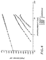
- Figure 4 illustrates that the output power as a function of photocurrent is nearly linear for each of the fundamental and the first three harmonics. All of the measurements are highly linear in form, and all of the harmonics are less than 60 dB at 5 mA of photocurrent over the frequency band of 15 GHz.
- the third intercept of the photodetector was measured to be 22 dBm. Additionally, the dc current voltage characteristics and the capacitance of the photodetector measured at -5V are less than 10 nanoamperes with a breakdown voltage of less than 20 volts, and 100 fF, respectively. The dc responsivity of the photodetector is 0.8 A/W.
Landscapes
- Light Receiving Elements (AREA)
- Photometry And Measurement Of Optical Pulse Characteristics (AREA)
- Radiation Pyrometers (AREA)
- Solid State Image Pick-Up Elements (AREA)
Applications Claiming Priority (2)
| Application Number | Priority Date | Filing Date | Title |
|---|---|---|---|
| US311673 | 1999-05-13 | ||
| US09/311,673 US6228673B1 (en) | 1999-05-13 | 1999-05-13 | Method of fabricating a surface coupled InGaAs photodetector |
Publications (3)
| Publication Number | Publication Date |
|---|---|
| EP1063709A2 true EP1063709A2 (de) | 2000-12-27 |
| EP1063709A3 EP1063709A3 (de) | 2001-09-26 |
| EP1063709B1 EP1063709B1 (de) | 2003-07-30 |
Family
ID=23207952
Family Applications (1)
| Application Number | Title | Priority Date | Filing Date |
|---|---|---|---|
| EP00109952A Expired - Lifetime EP1063709B1 (de) | 1999-05-13 | 2000-05-11 | Herstellungsverfahren für einen oberflächen-gekoppelten InGaAs Photodetektor |
Country Status (4)
| Country | Link |
|---|---|
| US (1) | US6228673B1 (de) |
| EP (1) | EP1063709B1 (de) |
| JP (1) | JP3662811B2 (de) |
| DE (1) | DE60004137T2 (de) |
Cited By (7)
| Publication number | Priority date | Publication date | Assignee | Title |
|---|---|---|---|---|
| EP1251565A3 (de) * | 2001-04-16 | 2007-05-23 | Sumitomo Electric Industries, Ltd. | Halbleiter lichtempfindliche Vorrichtung |
| US7767487B2 (en) | 2002-10-23 | 2010-08-03 | Ipl Intellectual Property Licensing Limited | Formation of contacts on semiconductor substrates |
| US7872237B2 (en) | 2002-10-25 | 2011-01-18 | Ipl Intellectual Property Licensing Limited | Circuit substrate and method |
| US8169522B2 (en) | 1994-06-01 | 2012-05-01 | Siemens Aktiengesellschaft | Imaging devices, systems and methods |
| RU2485628C1 (ru) * | 2012-01-19 | 2013-06-20 | Федеральное государственное бюджетное учреждение науки Физико-технический институт им. А.Ф. Иоффе Российской академии наук | Способ изготовления чипов наногетероструктуры и травитель |
| RU2530458C1 (ru) * | 2013-04-23 | 2014-10-10 | Российская Федерация, от имени которой выступает государственный заказчик - Министерство промышленности и торговли Российской Федерации | СПОСОБ ИЗГОТОВЛЕНИЯ МНОГОЭЛЕМЕНТНОГО ФОТОПРИЕМНИКА НА ОСНОВЕ ЭПИТАКСИАЛЬНЫХ СТРУКТУР InGaAs/InP |
| US9029793B2 (en) | 1998-11-05 | 2015-05-12 | Siemens Aktiengesellschaft | Imaging device |
Families Citing this family (9)
| Publication number | Priority date | Publication date | Assignee | Title |
|---|---|---|---|---|
| DE19956904C2 (de) * | 1999-11-26 | 2003-08-07 | United Monolithic Semiconduct | Integrierter Amplitudenbegrenzer bzw. Limiter und Verfahren zur Herstellung eines integrierten Limiters |
| US6780750B2 (en) * | 2002-01-08 | 2004-08-24 | Samsung Electronics Co. Ltd. | Photodiode for ultra high speed optical communication and fabrication method therefor |
| DE102004037868A1 (de) * | 2004-04-30 | 2005-11-24 | Osram Opto Semiconductors Gmbh | Strahlungsemittierendes und/oder -empfangendes Halbleiterbauelement und Verfahren zur strukturierten Aufbringung eines Kontakts auf einen Halbleiterkörper |
| US8072041B2 (en) * | 2009-04-08 | 2011-12-06 | Finisar Corporation | Passivated optical detectors with full protection layer |
| US9087926B2 (en) * | 2009-12-23 | 2015-07-21 | Avago Technologies General Ip (Singapore) Pte. Ltd. | Low capacitance semiconductor device |
| WO2015167524A1 (en) | 2014-04-30 | 2015-11-05 | Hewlett-Packard Development Company, L.P. | Mirrors including reflective and second layers disposed on photodetectors |
| CN105762226B (zh) * | 2014-12-19 | 2018-04-17 | 中国电子科技集团公司第十八研究所 | 一种多结太阳电池渐变缓冲层的腐蚀方法 |
| CN112582262B (zh) * | 2020-11-27 | 2022-10-04 | 中国电子科技集团公司第十三研究所 | 一种多层材料的非选择性湿法腐蚀方法及其应用 |
| US20230106167A1 (en) * | 2021-10-05 | 2023-04-06 | Arizona Board Of Regents On Behalf Of Arizona State University | De-bonding of thick films from carrier and methods thereof |
Family Cites Families (18)
| Publication number | Priority date | Publication date | Assignee | Title |
|---|---|---|---|---|
| US4414561A (en) * | 1979-09-27 | 1983-11-08 | Bell Telephone Laboratories, Incorporated | Beryllium-gold ohmic contact to a semiconductor device |
| FR2488049A1 (fr) * | 1980-07-31 | 1982-02-05 | Bouley Jean | Source lumineuse a jonction semiconductrice, notamment source-laser, utilisant des diodes schottky, et procede de fabrication |
| US4996163A (en) * | 1988-02-29 | 1991-02-26 | Sumitomo Electric Industries, Ltd. | Method for producing an opto-electronic integrated circuit |
| US5250471A (en) * | 1988-12-26 | 1993-10-05 | The Furukawa Electric Co. | Method for manufacturing compound semiconductor devices including a step where the semiconductor is etched without exposure to light |
| NL8902292A (nl) * | 1989-09-14 | 1991-04-02 | Philips Nv | Werkwijze voor het vervaardigen van een een mesa bevattende halfgeleiderinrichting. |
| US5365087A (en) * | 1992-07-15 | 1994-11-15 | Sumitomo Electric Industries, Ltd. | Photodetector and opto-electronic integrated circuit with guard ring |
| US5448099A (en) * | 1993-03-04 | 1995-09-05 | Sumitomo Electric Industries, Ltd. | Pin-type light receiving device, manufacture of the pin-type light receiving device and optoelectronic integrated circuit |
| JP3115148B2 (ja) * | 1993-03-31 | 2000-12-04 | 株式会社東芝 | 半導体装置の製造方法 |
| JP3191835B2 (ja) * | 1993-05-17 | 2001-07-23 | 住友電気工業株式会社 | 光電子集積回路 |
| JPH07211692A (ja) * | 1994-01-12 | 1995-08-11 | Sumitomo Electric Ind Ltd | InP系化合物半導体の加工方法 |
| JP2762939B2 (ja) * | 1994-03-22 | 1998-06-11 | 日本電気株式会社 | 超格子アバランシェフォトダイオード |
| US5518934A (en) * | 1994-07-21 | 1996-05-21 | Trustees Of Princeton University | Method of fabricating multiwavelength infrared focal plane array detector |
| EP0725447B1 (de) * | 1995-02-02 | 2007-11-14 | Sumitomo Electric Industries, Ltd. | PIN lichtempfindliche Vorrichtung und ihr Herstellungsverfahren |
| US5646069A (en) * | 1995-06-07 | 1997-07-08 | Hughes Aircraft Company | Fabrication process for Alx In1-x As/Gay In1-y As power HFET ohmic contacts |
| US5689122A (en) * | 1995-08-14 | 1997-11-18 | Lucent Technologies Inc. | InP/InGaAs monolithic integrated demultiplexer, photodetector, and heterojunction bipolar transistor |
| US5684308A (en) * | 1996-02-15 | 1997-11-04 | Sandia Corporation | CMOS-compatible InP/InGaAs digital photoreceiver |
| US6005266A (en) * | 1997-03-13 | 1999-12-21 | The Trustees Of Princeton University | Very low leakage JFET for monolithically integrated arrays |
| US5966622A (en) * | 1997-10-08 | 1999-10-12 | Lucent Technologies Inc. | Process for bonding crystalline substrates with different crystal lattices |
-
1999
- 1999-05-13 US US09/311,673 patent/US6228673B1/en not_active Expired - Lifetime
-
2000
- 2000-05-11 JP JP2000138348A patent/JP3662811B2/ja not_active Expired - Lifetime
- 2000-05-11 DE DE60004137T patent/DE60004137T2/de not_active Expired - Lifetime
- 2000-05-11 EP EP00109952A patent/EP1063709B1/de not_active Expired - Lifetime
Cited By (8)
| Publication number | Priority date | Publication date | Assignee | Title |
|---|---|---|---|---|
| US8169522B2 (en) | 1994-06-01 | 2012-05-01 | Siemens Aktiengesellschaft | Imaging devices, systems and methods |
| US9029793B2 (en) | 1998-11-05 | 2015-05-12 | Siemens Aktiengesellschaft | Imaging device |
| EP1251565A3 (de) * | 2001-04-16 | 2007-05-23 | Sumitomo Electric Industries, Ltd. | Halbleiter lichtempfindliche Vorrichtung |
| US7767487B2 (en) | 2002-10-23 | 2010-08-03 | Ipl Intellectual Property Licensing Limited | Formation of contacts on semiconductor substrates |
| USRE43948E1 (en) | 2002-10-23 | 2013-01-29 | Siemens Aktiengesellschaft | Formation of contacts on semiconductor substrates |
| US7872237B2 (en) | 2002-10-25 | 2011-01-18 | Ipl Intellectual Property Licensing Limited | Circuit substrate and method |
| RU2485628C1 (ru) * | 2012-01-19 | 2013-06-20 | Федеральное государственное бюджетное учреждение науки Физико-технический институт им. А.Ф. Иоффе Российской академии наук | Способ изготовления чипов наногетероструктуры и травитель |
| RU2530458C1 (ru) * | 2013-04-23 | 2014-10-10 | Российская Федерация, от имени которой выступает государственный заказчик - Министерство промышленности и торговли Российской Федерации | СПОСОБ ИЗГОТОВЛЕНИЯ МНОГОЭЛЕМЕНТНОГО ФОТОПРИЕМНИКА НА ОСНОВЕ ЭПИТАКСИАЛЬНЫХ СТРУКТУР InGaAs/InP |
Also Published As
| Publication number | Publication date |
|---|---|
| EP1063709B1 (de) | 2003-07-30 |
| US6228673B1 (en) | 2001-05-08 |
| JP2000353819A (ja) | 2000-12-19 |
| DE60004137T2 (de) | 2004-04-22 |
| DE60004137D1 (de) | 2003-09-04 |
| JP3662811B2 (ja) | 2005-06-22 |
| EP1063709A3 (de) | 2001-09-26 |
Similar Documents
| Publication | Publication Date | Title |
|---|---|---|
| US6228673B1 (en) | Method of fabricating a surface coupled InGaAs photodetector | |
| Ito et al. | Continuous THz-wave generation using antenna-integrated uni-travelling-carrier photodiodes | |
| CN106098836B (zh) | 通讯用雪崩光电二极管及其制备方法 | |
| JP5109981B2 (ja) | 半導体受光素子 | |
| US5281542A (en) | Planar quantum well photodetector | |
| US5448099A (en) | Pin-type light receiving device, manufacture of the pin-type light receiving device and optoelectronic integrated circuit | |
| JP2599131B2 (ja) | 集積光検出器−増幅器装置 | |
| KR100386905B1 (ko) | 금속-반도체-금속광검출기 | |
| Ünlü et al. | High bandwidth-efficiency resonant cavity enhanced Schottky photodiodes for 800–850 nm wavelength operation | |
| Duan et al. | Detrimental effect of impact ionization in the absorption region on the frequency response and excess noise performance of InGaAs-InAlAs SACM avalanche photodiodes | |
| US20250221059A1 (en) | Light Receiving Element | |
| Chizh et al. | High-speed high-power InAlAs/InGaAs/InP schottky photodiode | |
| US4894703A (en) | Restricted contact, planar photodiode | |
| Berger et al. | In0. 53Ga0. 47As p‐i‐n photodiodes with transparent cadmium tin oxide contacts | |
| KR100464367B1 (ko) | 포토다이오드 디텍터 및 그 제조방법 | |
| Jang et al. | The impact of a large bandgap drift region in long-wavelength metamorphic photodiodes | |
| Park et al. | High-performance InGaAs/InP avalanche photodiode for a 2.5 Gb s-1 optical receiver | |
| Unterborsch et al. | High-bandwidth 1.55/spl mu/m waveguide integrated photodetector | |
| Wang et al. | An 850 nm InGaAs Modified Uni-Traveling-Carrier Photodiode Enhanced by Distributed Bragg Reflector | |
| Chizh et al. | High-Power InGaAs/InAlAs schottky photodiode with low amplitude-to-phase noise conversion | |
| KR100654014B1 (ko) | 대구경 수광부를 위한 전극구조를 구비한 포토 다이오드 | |
| Miura et al. | Planar embedded InP/GaInAs pin photodiode for very high-speed operation | |
| Lo et al. | High-speed GaAs-on-InP long wavelength transmitter OEICs | |
| CN220753451U (zh) | 响应850nm波段的单行载流子光探测器芯片 | |
| Hurm et al. | Large area MSM photodiode array for 0.85 µm wavelength 10 Gbit/s per channel parallel optical links |
Legal Events
| Date | Code | Title | Description |
|---|---|---|---|
| PUAI | Public reference made under article 153(3) epc to a published international application that has entered the european phase |
Free format text: ORIGINAL CODE: 0009012 |
|
| AK | Designated contracting states |
Kind code of ref document: A2 Designated state(s): AT BE CH CY DE DK ES FI FR GB GR IE IT LI LU MC NL PT SE Kind code of ref document: A2 Designated state(s): DE FR GB IT |
|
| AX | Request for extension of the european patent |
Free format text: AL;LT;LV;MK;RO;SI |
|
| RIN1 | Information on inventor provided before grant (corrected) |
Inventor name: BROWN, JULIA, J. Inventor name: LOO, ROBERT, Y. Inventor name: SCHMITZ, ADELE, E. |
|
| PUAL | Search report despatched |
Free format text: ORIGINAL CODE: 0009013 |
|
| AK | Designated contracting states |
Kind code of ref document: A3 Designated state(s): AT BE CH CY DE DK ES FI FR GB GR IE IT LI LU MC NL PT SE |
|
| AX | Request for extension of the european patent |
Free format text: AL;LT;LV;MK;RO;SI |
|
| RIC1 | Information provided on ipc code assigned before grant |
Free format text: 7H 01L 31/18 A, 7H 01L 31/0304 B, 7H 01L 31/105 B |
|
| 17P | Request for examination filed |
Effective date: 20020306 |
|
| AKX | Designation fees paid |
Free format text: DE FR GB IT |
|
| GRAH | Despatch of communication of intention to grant a patent |
Free format text: ORIGINAL CODE: EPIDOS IGRA |
|
| 17Q | First examination report despatched |
Effective date: 20020903 |
|
| GRAH | Despatch of communication of intention to grant a patent |
Free format text: ORIGINAL CODE: EPIDOS IGRA |
|
| GRAA | (expected) grant |
Free format text: ORIGINAL CODE: 0009210 |
|
| AK | Designated contracting states |
Designated state(s): DE FR GB IT |
|
| REG | Reference to a national code |
Ref country code: GB Ref legal event code: FG4D |
|
| REF | Corresponds to: |
Ref document number: 60004137 Country of ref document: DE Date of ref document: 20030904 Kind code of ref document: P |
|
| ET | Fr: translation filed | ||
| PLBE | No opposition filed within time limit |
Free format text: ORIGINAL CODE: 0009261 |
|
| STAA | Information on the status of an ep patent application or granted ep patent |
Free format text: STATUS: NO OPPOSITION FILED WITHIN TIME LIMIT |
|
| 26N | No opposition filed |
Effective date: 20040504 |
|
| REG | Reference to a national code |
Ref country code: FR Ref legal event code: PLFP Year of fee payment: 17 |
|
| REG | Reference to a national code |
Ref country code: FR Ref legal event code: PLFP Year of fee payment: 18 |
|
| REG | Reference to a national code |
Ref country code: FR Ref legal event code: PLFP Year of fee payment: 19 |
|
| PGFP | Annual fee paid to national office [announced via postgrant information from national office to epo] |
Ref country code: IT Payment date: 20190523 Year of fee payment: 20 Ref country code: DE Payment date: 20190530 Year of fee payment: 20 |
|
| PGFP | Annual fee paid to national office [announced via postgrant information from national office to epo] |
Ref country code: FR Payment date: 20190527 Year of fee payment: 20 |
|
| PGFP | Annual fee paid to national office [announced via postgrant information from national office to epo] |
Ref country code: GB Payment date: 20190528 Year of fee payment: 20 |
|
| REG | Reference to a national code |
Ref country code: DE Ref legal event code: R071 Ref document number: 60004137 Country of ref document: DE |
|
| REG | Reference to a national code |
Ref country code: GB Ref legal event code: PE20 Expiry date: 20200510 |
|
| PG25 | Lapsed in a contracting state [announced via postgrant information from national office to epo] |
Ref country code: GB Free format text: LAPSE BECAUSE OF EXPIRATION OF PROTECTION Effective date: 20200510 |