EP1063823A2 - Système de reproduction des données pour téléphone portable - Google Patents
Système de reproduction des données pour téléphone portable Download PDFInfo
- Publication number
- EP1063823A2 EP1063823A2 EP00112960A EP00112960A EP1063823A2 EP 1063823 A2 EP1063823 A2 EP 1063823A2 EP 00112960 A EP00112960 A EP 00112960A EP 00112960 A EP00112960 A EP 00112960A EP 1063823 A2 EP1063823 A2 EP 1063823A2
- Authority
- EP
- European Patent Office
- Prior art keywords
- data
- portable telephone
- telephone set
- received signal
- signal
- Prior art date
- Legal status (The legal status is an assumption and is not a legal conclusion. Google has not performed a legal analysis and makes no representation as to the accuracy of the status listed.)
- Granted
Links
Images



Classifications
-
- H—ELECTRICITY
- H04—ELECTRIC COMMUNICATION TECHNIQUE
- H04L—TRANSMISSION OF DIGITAL INFORMATION, e.g. TELEGRAPHIC COMMUNICATION
- H04L27/00—Modulated-carrier systems
- H04L27/18—Phase-modulated carrier systems, i.e. using phase-shift keying
- H04L27/22—Demodulator circuits; Receiver circuits
- H04L27/233—Demodulator circuits; Receiver circuits using non-coherent demodulation
- H04L27/2332—Demodulator circuits; Receiver circuits using non-coherent demodulation using a non-coherent carrier
-
- H—ELECTRICITY
- H04—ELECTRIC COMMUNICATION TECHNIQUE
- H04L—TRANSMISSION OF DIGITAL INFORMATION, e.g. TELEGRAPHIC COMMUNICATION
- H04L27/00—Modulated-carrier systems
- H04L27/0014—Carrier regulation
- H04L2027/0024—Carrier regulation at the receiver end
- H04L2027/0026—Correction of carrier offset
- H04L2027/0028—Correction of carrier offset at passband only
-
- H—ELECTRICITY
- H04—ELECTRIC COMMUNICATION TECHNIQUE
- H04L—TRANSMISSION OF DIGITAL INFORMATION, e.g. TELEGRAPHIC COMMUNICATION
- H04L27/00—Modulated-carrier systems
- H04L27/0014—Carrier regulation
- H04L2027/0044—Control loops for carrier regulation
- H04L2027/0053—Closed loops
- H04L2027/0055—Closed loops single phase
Definitions
- the present invention relates to digital portable telephone sets and, more particularly, to digital portable telephone sets having a frequency deviation judging function.
- Fig. 4 is a schematic a prior art example of digital portable telephone set.
- the illustrated digital portable telephone set comprises an antenna 101, a radio unit 102, a demodulating unit 103, an automatic frequency control unit (hereinafter referred to as AFC unit) 104, a clock generating unit (hereinafter referred to as CLK unit) 105, a voice processing unit 106, a reference oscillator 108, a control unit 109, an operating unit 110, a display unit 111, a microphone (MIC) 112 and a receiver (REC) 113.
- AFC unit automatic frequency control unit
- CLK unit clock generating unit
- the radio unit 102 selects a signal frequency desired to be received from signal received by the antenna 101, and executes frequency conversion and amplification to provide an intermediate frequency signal (hereinafter referred to as IF signal) 161.
- the demodulator 103 demodulates the IF signal 161, and provides received data 162.
- the control unit 109 processes the received data 162, and provides a voice signal 163.
- the voice processing unit 106 converts the voice signal 163 to an analog signal to produce the voice through the receiver 113.
- the voice processing unit 106 converts voice 165 inputted from the microphone 112 to a digital signal, and the control unit 109 processes this digital data to provide transmission data.
- the radio unit 102 modulates the transmission data to generate a carrier wave at a prescribed frequency, and amplifies the generated carrier wave.
- the amplified carrier wave is transmitted from the antenna 101.
- the operating unit 110 is provided for inputting telephone number and other data, and it transfers the input data to the control unit 109.
- the display unit 111 displays various items.
- the CLK unit 105 generates a clock for timing processing, time instant display and so forth.
- the reference oscillator 108 generates a reference frequency used in a frequency generating unit in the radio unit 102 and an exact frequency used in the control unit 109 and the demodulating unit 103.
- the AFC unit 104 controls the reference oscillator 108 to obtain a frequency thereof identical with the exact frequency of the base station, which the signal is received from.
- the demodulating unit 103 will now be described.
- the digital portable telephone system adopts ⁇ /4 shift DQPSK (Differential Quadrature Phase Shift Keying) as modulating system.
- DQPSK Different Quadrature Phase Shift Keying
- Fig. 5 is a block diagram showing the example of the demodulating circuit in the delay detection system. This demodulating circuit is well known, and is not described in detail here.
- the demodulating unit 103 includes a phase detecting unit 121, a data (DATA) reproducing unit 122, a phase correcting unit 123, a clock reproducing unit (hereinafter referred to as CLK reproducing unit) 124 and a demodulating clock unit 125.
- DATA data
- CLK reproducing unit clock reproducing unit
- the phase detecting unit 121 provides an IF (intermediate frequency) signal from the radio unit 102 as phase data 129 under control of a clock of the reference frequency (or instance 14.4 MHZ) 128 at a timing of symbol clock 132.
- the data reproducing unit 122 produces received data 133 from the phase data 129, and provides the generated received data 133.
- the phase correcting unit 123 corrects the phase of the phase data 129, and provides a phase-corrected IF signal 130, which is used in the AFC unit 104.
- the demodulating CLK unit 125 has a PLL (Phase-Locked Loop) circuit construction, and provides a demodulating clock 181 (at 2.688 MHz, for instance) by using the reference frequency 128.
- the CLK reproducing unit 124 divides the frequency of the demodulating clock 181 to 1/128 to provide symbol clock 132 (at 21 kHz, for instance) and also to 1/64 to provide data clock (at 42 kHz, for instance).
- the unit 123 adjusts the phase timing of the symbol and data clocks 132 and 131 to be coincident with the symbol timing of the IF signal 127.
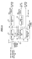
- FIG. 6 is a block diagram showing a first prior art example of data detecting circuit 122 used in a prior art delay detecting circuit. This prior art example is disclosed in detail in Japanese Patent Laid-Open No. 3-188737, and it is not described here in detail.
- a one symbol delaying unit 141 delays the phase data 129 from the phase detecting unit 121 by one symbol.
- a subtracter 142 subtracts delayed phase data 151 obtained by one symbol delaying and the phase data 129 from each other, and provides the difference as 5-bit phase difference data.
- a decoder 143 decodes the phase difference data 152, and converts the upper two bits and lower three bits of the result of decoding to received data 133a and quality data 133b, respectively.
- the received data 133a and quality data 133b are fed put as demodulation data 133 to the control unit 109.
- the quality data 133b is computationally processed in the control unit 109 for being used as frequency deviation detecting means.
- the control unit 109 operates the AFC unit 104.
- the control unit 109 further computationally processes the quality data 133b to generate quality data of the receiving line.
- the quality data is used as data means for line control in the portable telephone system.
- Fig. 7 is a block diagram showing the second prior art example of data reproducing unit 122.
- the second prior art example of data reproducing unit 122 shown in Fig. 7 has a feature that it can obtain good received frequency and is free from error factor deterioration irrespective of received frequency deviation.
- the principles underlying this second prior art example are described in detail in Japanese Patent Laid-Open No. 57-164645, and are not described here.
- the circuit construction of this example is described in detail in Japanese Patent Laid-Open No. 7-183927 and Japanese Patent Laid-Open No. 6-205062, and is not described in detail here.
- a correcting circuit 144 receives lower three bits (corresponding to quality data 133b) of phase difference data 152 provided from a subtracter 142, and calculates a phase difference due to the frequency deviation. The circuit 144 feeds the phase difference thus obtained as correcting value 153 back to the subtracter 142.
- no such process as feeding out lower three bits of the phase difference data 152 to the correcting circuit 144 is executed.
- Fig. 8 shows the construction of the correcting circuit 144 in the data reproducing unit 122.
- the correcting circuit 144 includes an accumulating unit 148 and an average calculating unit 149.
- the accumulating unit 148 accumulates lower three bits of the phase difference data 152 a number of symbol times, and feeds out the result of accumulation to the average calculating unit 149.
- the average calculating unit 149 calculates average data in a fixed symbol times number section, thereby feeding out the correcting value 153 to the subtracter 142.
- the second prior art example of data reproducing unit 122 has a drawback that it is incapable of computing the frequency deviation from the quality data 133b outputted from the decoder 143.
- this example has an advantageous feature that frequency deviation does not result in the received frequency deterioration or error factor deterioration, because the numerical value of the quality data 133b is not changed irrespective of frequency deviation, the control unit 109 can not detect frequency deviation by computing the quality data 133b. Consequently, the AFC unit 104 can not be started despite the fact that the frequency is deviated.
- An object of the present invention is to provide a digital portable telephone set capable of preventing received frequency deterioration and error factor deterioration in case of a received frequency deviation, and detecting a received frequency deviation, if any, to start the AFC unit for automatic frequency control, thus permitting satisfactory communication to be continued.
- a digital portable telephone set having demodulating means for demodulating a received signal
- the demodulating means includes data reproducing means, the data reproducing means having first data generating means for generating first quality data on the basis of the received signal, and second data generating means for generating second quality data different from the first quality data on the basis of the received signal.
- the first quality data includes received signal frequency data.
- the second quality data does not include the received signal frequency data.
- the second data generating means further generates received data on the basis of the received signal.
- the digital portable telephone set further comprises automatic frequency control means for automatically controlling the received signal frequency on the basis of the first quality data.
- the second data generating means includes a correcting circuit for correcting the received signal frequency data, and a decoder for generating the second quality data and the received data on the basis of new frequency data obtained in the correcting circuit.
- the correcting circuit corrects a frequency deviation of the received signal.
- the second quality data is used as line control data.
- a digital portable telephone set having demodulating means for demodulating a received signal
- the demodulating means includes data reproducing means, the data reproducing means having correcting means for correcting frequency data of the received signal, and data generating means for generating quality data on the basis of new frequency data obtained in the correcting means, corrected data obtained in the correcting means being used for received signal frequency control.
- the quality data includes received signal frequency data.
- the data generating means generates received data on the basis of the new frequency data.
- the digital portable telephone set further comprises automatic frequency control means for automatically controlling the received signal frequency according to the corrected data obtained in the correcting means.
- the correcting means corrects frequency deviation of the received signal.
- the quality data is used as line control data.
- a digital portable telephone set including means for demodulating a received signal and reproducing data with control means for line control in the portable telephone set comprising: a phase detecting unit for providing an IF signal from as phase data under control of a clock of the reference frequency at a timing of symbol clock; a one symbol delaying unit for delaying the phase data by one; a first subtracter for obtaining a first difference signal between the phase data and the delayed signal by the one symbol delaying unit; a second subtracter for obtaining a second difference signal between the phase data and the delayed signal by the one symbol delaying unit on the basis of a correction signal; a correcting means for producing the correction signal on the basis of the first difference signal; a first decoder for decoding the first difference signal to produce the received data and a first quality data of a reception line; and a second decoder for decoding the second difference signal to produce a second quality data of the reception line.
- a digital portable telephone set including means for demodulating a received signal and reproducing data, comprising: a phase detecting unit for providing an IF signal from as phase data under control of a clock of the reference frequency at a timing of symbol clock; a one symbol delaying unit for delaying the phase data by one; a subtracter for obtaining a difference signal between the delayed phase data obtained by one symbol delaying unit and the phase data on the basis of a correction signal; a decoder for decoding the difference signal to produce the received data and a quality data of a receipt line; a correcting means for producing the correction signal on the basis of the difference signal and supplying the correction signal.
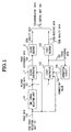
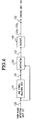
- Fig. 1 is a block diagram showing a first embodiment of the digital portable telephone set according to the present invention.
- Fig. 1 only the construction of a data reproducing unit in the digital portable telephone set is shown for the sake of convenience. This is so because the features of the present invention reside in the construction of the data reproducing unit.
- the construction of the digital portable telephone set which is like that in the prior art (see Fig. 4) and the construction of the demodulating unit (see Fig. 5) are not shown, and also their operations are not described.
- a data reproducing unit 122 comprises a one symbol delaying unit 141, a first subtracter 142, a first decoder 143, a correcting circuit 144, a second subtracter 1 and a second decoder 2.
- the correcting circuit 144 is connected to the first subtracter 142.
- the first subtracter 142 feeds out its output (i.e., first phase difference data) 152 to the first decoder 142.
- the first decoder 143 transfers upper two bits and lower three bits of its input as received data 113a and quality control data 132b, respectively, to control unit 109.
- the control unit 109 executes a computational process on the quality data 133b in the demodulation data 133 to generate quality data of the receiving line.
- the unit 109 makes the quality data 133b to be data means for line control in the portable telephone set.
- This circuit is the same in construction as the second prior art example (see Fig. 7), and its output thus has the same features as in the second prior art example.
- the received data thus has good receiving sensitivity and is free from error factor deterioration irrespective of frequency deviation.
- the second subtracter 1 in this circuit is free from any correcting circuit, and its output (i.e., second phase difference data 154) is fed out to the second decoder 2.
- the second decoder 2 converts lower three bits of its input to quality data 133a, and transfers this data as demodulation data 133 together with the received data 133a and quality data 133b to the control unit 109.
- the quality data 133c is obtained with the same circuit construction as the first prior art example (see Fig. 6), and thus it has the same features as the quality data 133b in the first prior art example. In other words, the value of the quality data 133c is changed by a frequency deviation.
- the controller 109 thus can check frequency deviation by computationally processing the quality data 133c, and it can drive the AFC unit 104.
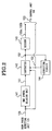
- FIG. 2 is a block diagram showing the second embodiment of the digital portable telephone set according to the present invention.
- Fig. 2 again only the construction of data reproducing unit in the digital portable telephone set is shown for the sake of convenience. This is so for the same reason as in the first embodiment.,
- the first embodiment has the subtracters and decoders dually, and it is thus correspondingly complicated in construction.
- the second embodiment improves this drawback, and features a simpler circuit construction.
- the second embodiment comprises a one symbol delaying unit 141, a subtracter 142, a decoder 143 and a correcting circuit 144.
- the second embodiment is the same in construction and the second prior art example (see Fig. 7).
- a difference resides in the output of the correcting circuit 144.
- this embodiment is different from the second prior art example in that corrected value 153, i.e., output of the correcting circuit 144, is transferred as demodulation data 133 together with the received data 133a and quality data 133b to control unit 109.
- the corrected value 153 features in its change with a frequency deviation.
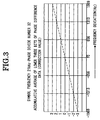
- Fig. 3 shows the relation between the accumulative average of the lower three bits of the phase difference data, i.e., "corrected value”, and the frequency deviation. From the Figure, it will be seen that the phase difference data lower three-bit accumulative average, i.e., "corrected value”, and the frequency deviation (in Hz) are proportional to each other. That is, the frequency deviation (in Hz) can be determined when the phase difference data lower three-bit accumulative average, i.e., "corrected value", is determined. In this embodiment, this feature is made use of. Specifically, the control unit 109 detects the frequency deviation by computing the corrected value 153, and then starts the AFC unit 104.
- the demodulating means includes data reproducing means, which has first data generating means for generating first quality data on the basis of the received signal and second data generating means for generating second quality data different from the first quality data on the basis of the received signal. It is thus possible to provide data for computing the frequency deviation together with the quality data. Thus, it is possible to prevent the receiving sensitivity deterioration or error factor deterioration irrespective of the received frequency deviation. Also, by detecting a received frequency deviation, if any, the AFC unit can be started for automatic frequency control to permit satisfactory communication to be continued.
- the demodulating means includes data reproducing means, which has correcting means for correcting frequency data of the received signal and data generating means for generating quality data according to the frequency data obtained in the correcting means, and the corrected value obtained in the correcting means is provided for received frequency control. It is thus possible to obtain the same effects as according to the first-mentioned aspect of the present invention.
Landscapes
- Engineering & Computer Science (AREA)
- Computer Networks & Wireless Communication (AREA)
- Signal Processing (AREA)
- Circuits Of Receivers In General (AREA)
- Digital Transmission Methods That Use Modulated Carrier Waves (AREA)
- Mobile Radio Communication Systems (AREA)
- Telephone Function (AREA)
Applications Claiming Priority (2)
| Application Number | Priority Date | Filing Date | Title |
|---|---|---|---|
| JP17617099 | 1999-06-23 | ||
| JP17617099A JP3735488B2 (ja) | 1999-06-23 | 1999-06-23 | デジタル携帯電話装置 |
Publications (3)
| Publication Number | Publication Date |
|---|---|
| EP1063823A2 true EP1063823A2 (fr) | 2000-12-27 |
| EP1063823A3 EP1063823A3 (fr) | 2003-12-10 |
| EP1063823B1 EP1063823B1 (fr) | 2006-03-01 |
Family
ID=16008897
Family Applications (1)
| Application Number | Title | Priority Date | Filing Date |
|---|---|---|---|
| EP00112960A Expired - Lifetime EP1063823B1 (fr) | 1999-06-23 | 2000-06-20 | Système de reproduction des données pour téléphone portable |
Country Status (6)
| Country | Link |
|---|---|
| US (1) | US7197136B1 (fr) |
| EP (1) | EP1063823B1 (fr) |
| JP (1) | JP3735488B2 (fr) |
| CN (1) | CN1279573A (fr) |
| AU (1) | AU765678B2 (fr) |
| DE (1) | DE60026202T2 (fr) |
Families Citing this family (1)
| Publication number | Priority date | Publication date | Assignee | Title |
|---|---|---|---|---|
| KR102510515B1 (ko) * | 2016-03-07 | 2023-03-16 | 삼성전자주식회사 | Sof 패턴에 기초하여 분석된 수신 특성을 참조하여 데이터를 디코딩하도록 구성되는 통신 회로 칩 및 전자 장치 |
Family Cites Families (17)
| Publication number | Priority date | Publication date | Assignee | Title |
|---|---|---|---|---|
| JPS57164645A (en) | 1981-04-03 | 1982-10-09 | Nec Corp | Delay detecting circuit |
| JP2504243B2 (ja) | 1989-12-18 | 1996-06-05 | 日本電気株式会社 | 復調方式 |
| JPH03274844A (ja) | 1990-03-24 | 1991-12-05 | Japan Radio Co Ltd | Psk変調信号の遅延検波回路 |
| JPH0642685B2 (ja) | 1990-07-05 | 1994-06-01 | 日本無線株式会社 | 遅延検波回路 |
| JPH06205062A (ja) | 1993-01-08 | 1994-07-22 | Nec Corp | 遅延検波回路 |
| JPH06268696A (ja) | 1993-03-10 | 1994-09-22 | Toyo Commun Equip Co Ltd | Afc回路 |
| JPH07183927A (ja) | 1993-12-24 | 1995-07-21 | Nec Corp | 多相位相変調信号の遅延検波装置 |
| JPH07242260A (ja) | 1994-03-01 | 1995-09-19 | Masuhiro Mitsuyama | レンタル商品の盗難防止装置 |
| JPH07264009A (ja) | 1994-03-16 | 1995-10-13 | Kenji Harada | 自動周波数制御装置 |
| JPH07297779A (ja) | 1994-04-26 | 1995-11-10 | Toshiba Corp | 自動周波数制御機能を備えたディジタル無線機 |
| US5479452A (en) * | 1994-09-06 | 1995-12-26 | Motorola, Inc. | Method and apparatus for aligning a digital receiver |
| JPH08139663A (ja) | 1994-11-09 | 1996-05-31 | Nippon Ido Tsushin Kk | 移動通信端末 |
| JP3178281B2 (ja) | 1994-12-13 | 2001-06-18 | 三菱電機株式会社 | 自動周波数制御復調装置 |
| JP3130773B2 (ja) * | 1995-10-16 | 2001-01-31 | 日本電気株式会社 | 無線データ通信の復調装置 |
| JPH09162936A (ja) | 1995-12-11 | 1997-06-20 | Nec Corp | 周波数オフセット補正機能付き通信装置 |
| NO318992B1 (no) | 1996-03-06 | 2005-05-30 | Matsushita Electric Industrial Co Ltd | Differensialdetekteringsmottaker |
| FI106680B (fi) * | 1996-06-17 | 2001-03-15 | Nokia Mobile Phones Ltd | Menetelmä vastaanoton laadun parantamiseksi radiovastaanottimessa ja radiovastaanotin |
-
1999
- 1999-06-23 JP JP17617099A patent/JP3735488B2/ja not_active Expired - Fee Related
-
2000
- 2000-06-15 US US09/595,494 patent/US7197136B1/en not_active Expired - Fee Related
- 2000-06-20 EP EP00112960A patent/EP1063823B1/fr not_active Expired - Lifetime
- 2000-06-20 AU AU42542/00A patent/AU765678B2/en not_active Ceased
- 2000-06-20 DE DE60026202T patent/DE60026202T2/de not_active Expired - Fee Related
- 2000-06-23 CN CN00122267A patent/CN1279573A/zh active Pending
Also Published As
| Publication number | Publication date |
|---|---|
| US7197136B1 (en) | 2007-03-27 |
| JP3735488B2 (ja) | 2006-01-18 |
| AU765678B2 (en) | 2003-09-25 |
| DE60026202T2 (de) | 2006-11-23 |
| CN1279573A (zh) | 2001-01-10 |
| JP2001007725A (ja) | 2001-01-12 |
| EP1063823A3 (fr) | 2003-12-10 |
| AU4254200A (en) | 2001-01-04 |
| EP1063823B1 (fr) | 2006-03-01 |
| DE60026202D1 (de) | 2006-04-27 |
Similar Documents
| Publication | Publication Date | Title |
|---|---|---|
| US6571088B1 (en) | Automatic frequency control circuit | |
| EP0726662A3 (fr) | Récepteur et émetteur-récepteur | |
| US5457716A (en) | Automatic frequency control in a radio communication receiver | |
| JP3141589B2 (ja) | 受信機で用いるためのデータ信号補償装置 | |
| US6078578A (en) | Communication apparatus | |
| JPH1117750A (ja) | 自動周波数制御装置 | |
| EP0919084B1 (fr) | Dispositif de communication numerique | |
| WO1995006362A1 (fr) | Compensation de la frequence de reference | |
| US7197136B1 (en) | Digital portable telephone set | |
| US6389303B1 (en) | Booster for amplifying the transmission output of a handy phone | |
| US6618459B1 (en) | Radio communication device and method of bit synchronization pull-in in the same | |
| JP4835172B2 (ja) | 無線通信機及びその自動周波数制御方法 | |
| EP1109318A1 (fr) | Controleur de boucle a phase asservie, procede de controle de boucle a phase asservie et limiteur | |
| JP2639326B2 (ja) | 四値fsk受信機 | |
| JP3398689B2 (ja) | デジタル携帯電話装置 | |
| US20020190803A1 (en) | AFC circuit | |
| JPH06164531A (ja) | Tdma受信フレーム同期方式 | |
| US6587523B1 (en) | Radio signal receiving apparatus and a method of radio signal reception | |
| JP3381663B2 (ja) | 周波数ズレ自動補正復調装置及び周波数ズレ自動補正復調方法 | |
| JP3057198B2 (ja) | 無線通信方式 | |
| JPH0779265A (ja) | 復調回路及び復調方法 | |
| JP2974296B2 (ja) | 無線選択呼出受信機 | |
| JPH09247220A (ja) | 自動周波数制御回路 | |
| JP2896638B2 (ja) | Qam復調装置 | |
| JP2002016481A (ja) | 自動周波数制御方式 |
Legal Events
| Date | Code | Title | Description |
|---|---|---|---|
| PUAI | Public reference made under article 153(3) epc to a published international application that has entered the european phase |
Free format text: ORIGINAL CODE: 0009012 |
|
| AK | Designated contracting states |
Kind code of ref document: A2 Designated state(s): AT BE CH CY DE DK ES FI FR GB GR IE IT LI LU MC NL PT SE |
|
| AX | Request for extension of the european patent |
Free format text: AL;LT;LV;MK;RO;SI |
|
| PUAL | Search report despatched |
Free format text: ORIGINAL CODE: 0009013 |
|
| AK | Designated contracting states |
Kind code of ref document: A3 Designated state(s): AT BE CH CY DE DK ES FI FR GB GR IE IT LI LU MC NL PT SE |
|
| AX | Request for extension of the european patent |
Extension state: AL LT LV MK RO SI |
|
| 17P | Request for examination filed |
Effective date: 20031027 |
|
| 17Q | First examination report despatched |
Effective date: 20040714 |
|
| AKX | Designation fees paid |
Designated state(s): DE FR GB IT |
|
| GRAP | Despatch of communication of intention to grant a patent |
Free format text: ORIGINAL CODE: EPIDOSNIGR1 |
|
| GRAS | Grant fee paid |
Free format text: ORIGINAL CODE: EPIDOSNIGR3 |
|
| GRAA | (expected) grant |
Free format text: ORIGINAL CODE: 0009210 |
|
| AK | Designated contracting states |
Kind code of ref document: B1 Designated state(s): DE FR GB IT |
|
| REG | Reference to a national code |
Ref country code: GB Ref legal event code: FG4D |
|
| REF | Corresponds to: |
Ref document number: 60026202 Country of ref document: DE Date of ref document: 20060427 Kind code of ref document: P |
|
| ET | Fr: translation filed | ||
| PLBE | No opposition filed within time limit |
Free format text: ORIGINAL CODE: 0009261 |
|
| STAA | Information on the status of an ep patent application or granted ep patent |
Free format text: STATUS: NO OPPOSITION FILED WITHIN TIME LIMIT |
|
| 26N | No opposition filed |
Effective date: 20061204 |
|
| PGFP | Annual fee paid to national office [announced via postgrant information from national office to epo] |
Ref country code: IT Payment date: 20090622 Year of fee payment: 10 |
|
| PGFP | Annual fee paid to national office [announced via postgrant information from national office to epo] |
Ref country code: GB Payment date: 20090617 Year of fee payment: 10 Ref country code: DE Payment date: 20090619 Year of fee payment: 10 |
|
| GBPC | Gb: european patent ceased through non-payment of renewal fee |
Effective date: 20100620 |
|
| REG | Reference to a national code |
Ref country code: FR Ref legal event code: ST Effective date: 20110228 |
|
| PG25 | Lapsed in a contracting state [announced via postgrant information from national office to epo] |
Ref country code: IT Free format text: LAPSE BECAUSE OF NON-PAYMENT OF DUE FEES Effective date: 20100620 |
|
| PG25 | Lapsed in a contracting state [announced via postgrant information from national office to epo] |
Ref country code: DE Free format text: LAPSE BECAUSE OF NON-PAYMENT OF DUE FEES Effective date: 20110101 |
|
| PG25 | Lapsed in a contracting state [announced via postgrant information from national office to epo] |
Ref country code: FR Free format text: LAPSE BECAUSE OF NON-PAYMENT OF DUE FEES Effective date: 20100630 |
|
| PG25 | Lapsed in a contracting state [announced via postgrant information from national office to epo] |
Ref country code: GB Free format text: LAPSE BECAUSE OF NON-PAYMENT OF DUE FEES Effective date: 20100620 |
|
| PGFP | Annual fee paid to national office [announced via postgrant information from national office to epo] |
Ref country code: FR Payment date: 20090611 Year of fee payment: 10 |