EP1065712A1 - Méthode de soudure de fil dans un dispositif semiconducteur - Google Patents
Méthode de soudure de fil dans un dispositif semiconducteur Download PDFInfo
- Publication number
- EP1065712A1 EP1065712A1 EP00113595A EP00113595A EP1065712A1 EP 1065712 A1 EP1065712 A1 EP 1065712A1 EP 00113595 A EP00113595 A EP 00113595A EP 00113595 A EP00113595 A EP 00113595A EP 1065712 A1 EP1065712 A1 EP 1065712A1
- Authority
- EP
- European Patent Office
- Prior art keywords
- conductive member
- wire
- semiconductor chip
- lower conductive
- conductive
- Prior art date
- Legal status (The legal status is an assumption and is not a legal conclusion. Google has not performed a legal analysis and makes no representation as to the accuracy of the status listed.)
- Ceased
Links
Images


Classifications
-
- H—ELECTRICITY
- H10—SEMICONDUCTOR DEVICES; ELECTRIC SOLID-STATE DEVICES NOT OTHERWISE PROVIDED FOR
- H10W—GENERIC PACKAGES, INTERCONNECTIONS, CONNECTORS OR OTHER CONSTRUCTIONAL DETAILS OF DEVICES COVERED BY CLASS H10
- H10W72/00—Interconnections or connectors in packages
- H10W72/071—Connecting or disconnecting
- H10W72/075—Connecting or disconnecting of bond wires
-
- H—ELECTRICITY
- H10—SEMICONDUCTOR DEVICES; ELECTRIC SOLID-STATE DEVICES NOT OTHERWISE PROVIDED FOR
- H10W—GENERIC PACKAGES, INTERCONNECTIONS, CONNECTORS OR OTHER CONSTRUCTIONAL DETAILS OF DEVICES COVERED BY CLASS H10
- H10W72/00—Interconnections or connectors in packages
- H10W72/071—Connecting or disconnecting
- H10W72/0711—Apparatus therefor
-
- H—ELECTRICITY
- H10—SEMICONDUCTOR DEVICES; ELECTRIC SOLID-STATE DEVICES NOT OTHERWISE PROVIDED FOR
- H10W—GENERIC PACKAGES, INTERCONNECTIONS, CONNECTORS OR OTHER CONSTRUCTIONAL DETAILS OF DEVICES COVERED BY CLASS H10
- H10W72/00—Interconnections or connectors in packages
- H10W72/50—Bond wires
-
- H—ELECTRICITY
- H10—SEMICONDUCTOR DEVICES; ELECTRIC SOLID-STATE DEVICES NOT OTHERWISE PROVIDED FOR
- H10W—GENERIC PACKAGES, INTERCONNECTIONS, CONNECTORS OR OTHER CONSTRUCTIONAL DETAILS OF DEVICES COVERED BY CLASS H10
- H10W72/00—Interconnections or connectors in packages
- H10W72/01—Manufacture or treatment
- H10W72/015—Manufacture or treatment of bond wires
- H10W72/01551—Changing the shapes of bond wires
-
- H—ELECTRICITY
- H10—SEMICONDUCTOR DEVICES; ELECTRIC SOLID-STATE DEVICES NOT OTHERWISE PROVIDED FOR
- H10W—GENERIC PACKAGES, INTERCONNECTIONS, CONNECTORS OR OTHER CONSTRUCTIONAL DETAILS OF DEVICES COVERED BY CLASS H10
- H10W72/00—Interconnections or connectors in packages
- H10W72/071—Connecting or disconnecting
- H10W72/0711—Apparatus therefor
- H10W72/07141—Means for applying energy, e.g. ovens or lasers
-
- H—ELECTRICITY
- H10—SEMICONDUCTOR DEVICES; ELECTRIC SOLID-STATE DEVICES NOT OTHERWISE PROVIDED FOR
- H10W—GENERIC PACKAGES, INTERCONNECTIONS, CONNECTORS OR OTHER CONSTRUCTIONAL DETAILS OF DEVICES COVERED BY CLASS H10
- H10W72/00—Interconnections or connectors in packages
- H10W72/071—Connecting or disconnecting
- H10W72/075—Connecting or disconnecting of bond wires
- H10W72/07502—Connecting or disconnecting of bond wires using an auxiliary member
-
- H—ELECTRICITY
- H10—SEMICONDUCTOR DEVICES; ELECTRIC SOLID-STATE DEVICES NOT OTHERWISE PROVIDED FOR
- H10W—GENERIC PACKAGES, INTERCONNECTIONS, CONNECTORS OR OTHER CONSTRUCTIONAL DETAILS OF DEVICES COVERED BY CLASS H10
- H10W72/00—Interconnections or connectors in packages
- H10W72/071—Connecting or disconnecting
- H10W72/075—Connecting or disconnecting of bond wires
- H10W72/07511—Treating the bonding area before connecting, e.g. by applying flux or cleaning
-
- H—ELECTRICITY
- H10—SEMICONDUCTOR DEVICES; ELECTRIC SOLID-STATE DEVICES NOT OTHERWISE PROVIDED FOR
- H10W—GENERIC PACKAGES, INTERCONNECTIONS, CONNECTORS OR OTHER CONSTRUCTIONAL DETAILS OF DEVICES COVERED BY CLASS H10
- H10W72/00—Interconnections or connectors in packages
- H10W72/071—Connecting or disconnecting
- H10W72/075—Connecting or disconnecting of bond wires
- H10W72/07521—Aligning
-
- H—ELECTRICITY
- H10—SEMICONDUCTOR DEVICES; ELECTRIC SOLID-STATE DEVICES NOT OTHERWISE PROVIDED FOR
- H10W—GENERIC PACKAGES, INTERCONNECTIONS, CONNECTORS OR OTHER CONSTRUCTIONAL DETAILS OF DEVICES COVERED BY CLASS H10
- H10W72/00—Interconnections or connectors in packages
- H10W72/071—Connecting or disconnecting
- H10W72/075—Connecting or disconnecting of bond wires
- H10W72/07531—Techniques
- H10W72/07532—Compression bonding, e.g. thermocompression bonding
- H10W72/07533—Ultrasonic bonding, e.g. thermosonic bonding
-
- H—ELECTRICITY
- H10—SEMICONDUCTOR DEVICES; ELECTRIC SOLID-STATE DEVICES NOT OTHERWISE PROVIDED FOR
- H10W—GENERIC PACKAGES, INTERCONNECTIONS, CONNECTORS OR OTHER CONSTRUCTIONAL DETAILS OF DEVICES COVERED BY CLASS H10
- H10W72/00—Interconnections or connectors in packages
- H10W72/50—Bond wires
- H10W72/531—Shapes of wire connectors
- H10W72/536—Shapes of wire connectors the connected ends being ball-shaped
-
- H—ELECTRICITY
- H10—SEMICONDUCTOR DEVICES; ELECTRIC SOLID-STATE DEVICES NOT OTHERWISE PROVIDED FOR
- H10W—GENERIC PACKAGES, INTERCONNECTIONS, CONNECTORS OR OTHER CONSTRUCTIONAL DETAILS OF DEVICES COVERED BY CLASS H10
- H10W72/00—Interconnections or connectors in packages
- H10W72/50—Bond wires
- H10W72/531—Shapes of wire connectors
- H10W72/5363—Shapes of wire connectors the connected ends being wedge-shaped
-
- H—ELECTRICITY
- H10—SEMICONDUCTOR DEVICES; ELECTRIC SOLID-STATE DEVICES NOT OTHERWISE PROVIDED FOR
- H10W—GENERIC PACKAGES, INTERCONNECTIONS, CONNECTORS OR OTHER CONSTRUCTIONAL DETAILS OF DEVICES COVERED BY CLASS H10
- H10W72/00—Interconnections or connectors in packages
- H10W72/50—Bond wires
- H10W72/531—Shapes of wire connectors
- H10W72/5366—Shapes of wire connectors the bond wires having kinks
-
- H—ELECTRICITY
- H10—SEMICONDUCTOR DEVICES; ELECTRIC SOLID-STATE DEVICES NOT OTHERWISE PROVIDED FOR
- H10W—GENERIC PACKAGES, INTERCONNECTIONS, CONNECTORS OR OTHER CONSTRUCTIONAL DETAILS OF DEVICES COVERED BY CLASS H10
- H10W72/00—Interconnections or connectors in packages
- H10W72/50—Bond wires
- H10W72/541—Dispositions of bond wires
- H10W72/5434—Dispositions of bond wires the connected ends being on auxiliary connecting means on bond pads, e.g. on other bond wires
-
- H—ELECTRICITY
- H10—SEMICONDUCTOR DEVICES; ELECTRIC SOLID-STATE DEVICES NOT OTHERWISE PROVIDED FOR
- H10W—GENERIC PACKAGES, INTERCONNECTIONS, CONNECTORS OR OTHER CONSTRUCTIONAL DETAILS OF DEVICES COVERED BY CLASS H10
- H10W72/00—Interconnections or connectors in packages
- H10W72/50—Bond wires
- H10W72/541—Dispositions of bond wires
- H10W72/5445—Dispositions of bond wires being orthogonal to a side surface of the chip, e.g. parallel arrangements
-
- H—ELECTRICITY
- H10—SEMICONDUCTOR DEVICES; ELECTRIC SOLID-STATE DEVICES NOT OTHERWISE PROVIDED FOR
- H10W—GENERIC PACKAGES, INTERCONNECTIONS, CONNECTORS OR OTHER CONSTRUCTIONAL DETAILS OF DEVICES COVERED BY CLASS H10
- H10W72/00—Interconnections or connectors in packages
- H10W72/50—Bond wires
- H10W72/541—Dispositions of bond wires
- H10W72/547—Dispositions of multiple bond wires
- H10W72/5473—Dispositions of multiple bond wires multiple bond wires connected to a common bond pad
-
- H—ELECTRICITY
- H10—SEMICONDUCTOR DEVICES; ELECTRIC SOLID-STATE DEVICES NOT OTHERWISE PROVIDED FOR
- H10W—GENERIC PACKAGES, INTERCONNECTIONS, CONNECTORS OR OTHER CONSTRUCTIONAL DETAILS OF DEVICES COVERED BY CLASS H10
- H10W72/00—Interconnections or connectors in packages
- H10W72/50—Bond wires
- H10W72/551—Materials of bond wires
- H10W72/552—Materials of bond wires comprising metals or metalloids, e.g. silver
- H10W72/5522—Materials of bond wires comprising metals or metalloids, e.g. silver comprising gold [Au]
-
- H—ELECTRICITY
- H10—SEMICONDUCTOR DEVICES; ELECTRIC SOLID-STATE DEVICES NOT OTHERWISE PROVIDED FOR
- H10W—GENERIC PACKAGES, INTERCONNECTIONS, CONNECTORS OR OTHER CONSTRUCTIONAL DETAILS OF DEVICES COVERED BY CLASS H10
- H10W72/00—Interconnections or connectors in packages
- H10W72/50—Bond wires
- H10W72/581—Auxiliary members, e.g. flow barriers
- H10W72/583—Reinforcing structures
-
- H—ELECTRICITY
- H10—SEMICONDUCTOR DEVICES; ELECTRIC SOLID-STATE DEVICES NOT OTHERWISE PROVIDED FOR
- H10W—GENERIC PACKAGES, INTERCONNECTIONS, CONNECTORS OR OTHER CONSTRUCTIONAL DETAILS OF DEVICES COVERED BY CLASS H10
- H10W72/00—Interconnections or connectors in packages
- H10W72/50—Bond wires
- H10W72/59—Bond pads specially adapted therefor
-
- H—ELECTRICITY
- H10—SEMICONDUCTOR DEVICES; ELECTRIC SOLID-STATE DEVICES NOT OTHERWISE PROVIDED FOR
- H10W—GENERIC PACKAGES, INTERCONNECTIONS, CONNECTORS OR OTHER CONSTRUCTIONAL DETAILS OF DEVICES COVERED BY CLASS H10
- H10W72/00—Interconnections or connectors in packages
- H10W72/90—Bond pads, in general
- H10W72/931—Shapes of bond pads
- H10W72/932—Plan-view shape, i.e. in top view
-
- H—ELECTRICITY
- H10—SEMICONDUCTOR DEVICES; ELECTRIC SOLID-STATE DEVICES NOT OTHERWISE PROVIDED FOR
- H10W—GENERIC PACKAGES, INTERCONNECTIONS, CONNECTORS OR OTHER CONSTRUCTIONAL DETAILS OF DEVICES COVERED BY CLASS H10
- H10W72/00—Interconnections or connectors in packages
- H10W72/90—Bond pads, in general
- H10W72/951—Materials of bond pads
- H10W72/952—Materials of bond pads comprising metals or metalloids, e.g. PbSn, Ag or Cu
-
- H—ELECTRICITY
- H10—SEMICONDUCTOR DEVICES; ELECTRIC SOLID-STATE DEVICES NOT OTHERWISE PROVIDED FOR
- H10W—GENERIC PACKAGES, INTERCONNECTIONS, CONNECTORS OR OTHER CONSTRUCTIONAL DETAILS OF DEVICES COVERED BY CLASS H10
- H10W74/00—Encapsulations, e.g. protective coatings
-
- H—ELECTRICITY
- H10—SEMICONDUCTOR DEVICES; ELECTRIC SOLID-STATE DEVICES NOT OTHERWISE PROVIDED FOR
- H10W—GENERIC PACKAGES, INTERCONNECTIONS, CONNECTORS OR OTHER CONSTRUCTIONAL DETAILS OF DEVICES COVERED BY CLASS H10
- H10W90/00—Package configurations
- H10W90/701—Package configurations characterised by the relative positions of pads or connectors relative to package parts
- H10W90/751—Package configurations characterised by the relative positions of pads or connectors relative to package parts of bond wires
- H10W90/753—Package configurations characterised by the relative positions of pads or connectors relative to package parts of bond wires between laterally-adjacent chips
-
- H—ELECTRICITY
- H10—SEMICONDUCTOR DEVICES; ELECTRIC SOLID-STATE DEVICES NOT OTHERWISE PROVIDED FOR
- H10W—GENERIC PACKAGES, INTERCONNECTIONS, CONNECTORS OR OTHER CONSTRUCTIONAL DETAILS OF DEVICES COVERED BY CLASS H10
- H10W90/00—Package configurations
- H10W90/701—Package configurations characterised by the relative positions of pads or connectors relative to package parts
- H10W90/751—Package configurations characterised by the relative positions of pads or connectors relative to package parts of bond wires
- H10W90/754—Package configurations characterised by the relative positions of pads or connectors relative to package parts of bond wires between a chip and a stacked insulating package substrate, interposer or RDL
-
- H—ELECTRICITY
- H10—SEMICONDUCTOR DEVICES; ELECTRIC SOLID-STATE DEVICES NOT OTHERWISE PROVIDED FOR
- H10W—GENERIC PACKAGES, INTERCONNECTIONS, CONNECTORS OR OTHER CONSTRUCTIONAL DETAILS OF DEVICES COVERED BY CLASS H10
- H10W90/00—Package configurations
- H10W90/701—Package configurations characterised by the relative positions of pads or connectors relative to package parts
- H10W90/751—Package configurations characterised by the relative positions of pads or connectors relative to package parts of bond wires
- H10W90/756—Package configurations characterised by the relative positions of pads or connectors relative to package parts of bond wires between a chip and a stacked lead frame, conducting package substrate or heat sink
Definitions
- the present invention relates to a semiconductor device having a semiconductor chip and a wiring member to be electrically connected to the semiconductor chip and a method of manufacturing the semiconductor device.
- a semiconductor chip and a lead frame incorporating it are electrically connected by a bonding wire.
- a wire bonding step a ball is formed on the tip of a boning wire, the ball is fixed to the pad on a semiconductor chip.
- the bonding wire is extended onto the lead frame and connected a lead frame. Thereafter, the bonding wire is cut.
- Such a wire bonding technique is disclosed in e.g. JP-A-55-118643.
- the technique disclosed therein relates to a wire bonding technique of bonding an Au wire to an Al face.
- intermetallic compound will be generated at the interface therebetween and the boundary is made fragile so that the bonding strength becomes insufficient.
- the invention disclosed in the reference has been accomplished.
- the semiconductor device manufactured by the above technique cannot also provide sufficient bonding strength under its utilizing environment.
- the strength of wire bonding may be reduced according to the chemical state of the surface of the pad of a semiconductor chip, terminal of a package and lead frame.
- the bonding wire is broken when a smaller strength than the strength of a wire strand itself is applied.
- the inventors of the invention have found that where the wire bonding strength was reduced, the sectional area of the neck portion (just near a ball portion formed at the top end) of the bonding wire had been reduced. If expansion and shrinkage of mold resin of a resin-sealed semiconductor chip, which is thus wire-bonded in such a condition, great strength is applied to a bonding wire of the semiconductor chip. Therefore, the semiconductor device is failed at the portion having a smaller area of the bonding wire.
- An object of the invention is to provide a semiconductor device which can prevent reduction in the tension leading to breakage of a bonding wire and a method for manufacturing such a semiconductor device.
- a semiconductor device includes a lower conductive member, a upper conductive member and a conductive wire.
- the lower conductive member is formed on a wiring member to be electrically connected to the semiconductor chip.
- the one end of the conductive wire is electrically connected to a semiconductor chip.
- the other end of the conductive wire is sandwiched between the lower conductive member and the upper conductive member located thereon and is electrically connected to the wiring member.
- the semiconductor chip is electrically connected to the wiring member through the conductive wire.
- the connecting portion of the conductive wire to be connected to the wiring member is sandwiched between the lower and upper conductive members so that the neck portion of the conductive wire can be protected from above by the upper conductive member. Therefore, such a structure having both lower and upper conductive members has an increased bonding area of the conductive wire between both conductive members as compared with the structure provided with only the lower conductive member and hence provides an increased bonding strength. Further, the lower conductive member is formed on the lower side of the conductive wire. Therefore, in bonding, the lower conductive member is deformed so that deformation of the conductive wire itself is suppressed and reduction in the sectional area of the neck portion of the conductive wire is also suppressed.
- a semiconductor device includes a lower conductive member, a second connecting member and a conductive wire.
- the lower conductive member is formed on a wiring member to be electrically connected to a semiconductor chip.
- the second connecting member having a upper conductive member formed on said lower conductive member and a connecting portion connected to said wiring member at a different position from said lower conductive member.
- the one end of the conductive wire is electrically connected to said semiconductor chip.
- the other end of the conductive wire is sandwiched between said lower and upper conductive members and electrically connected to said lower conductive member.
- the neck portion is protected by the upper conductive member.
- the lower conductive member to which the other end of the conductive wire is bonded is bonded to the wiring member.
- the other end of the conductive wire is also bonded to the upper conductive member of the second connecting member.
- the second connecting member is bonded to the wiring member at a different position from the lower conductive member.
- the semiconductor device includes a first connecting member, a second connecting member and a conductive wire.
- the first connecting member has a lower conductive member formed on a wiring member to be electrically connected to a semiconductor chip and a connecting portion connected to the wiring member at a different position from said lower conductive member.
- the second connecting member has an upper conductive member formed on said lower conductive member and a connecting portion connected to said wiring member at a different position from said lower conductive member.
- the one end of the conductive wire is electrically connected to said semiconductor chip.
- the other end thereof is sandwiched between said lower and upper conductive member and electrically connected to said lower conductive member.
- the neck portion is protected by the upper conductive member.
- the other end of the conductive wire is bonded to the wiring member through the lower conductive member and also bonded to the upper conductive member of the second connecting member.
- the first and the second connecting member are bonded to the wiring member at different positions from the lower conductive member, respectively. Therefore, the conductive wire is connected to the wiring member through the lower conductive member and the first and the second connecting member.
- the bonding area between the conductive wire and the wiring member is increased so that bonding strength therebetween is increased.
- the tension applied to the conductive wire is dispersed at the plural connecting positions. Therefore, since the tension applied to each of the plural connecting positions is reduced on average, even if there is a distribution of the bonding strength, the margin for the limit of the strength leading to flaking of the bonding can be assured.
- the lower and the upper conductive member and the conductive wire are made of the same material. Because of a metallographic nature, the bonding strength will be made greater between the same kinds of metal than between the different kinds of metal. A wavelength of the light, which the light emitting element and the light receiving element has sensivity, is permeable to the mold resin.
- the semiconductor device according to the invention preferably includes mold resin for sealing the semiconductor chip and wiring member.
- the semiconductor chip can include at least one of a light emitting element and a light receiving element.
- the light relative to the light emitting element and light receiving element is preferably permeable to the mold resin.
- the semiconductor device is sealed by mold resin, its strength for the stress applied when the mold resin is expanded or shrunken can be increased.
- a semiconductor device is suitable when it is molded by transparent resin because the transparent resin and the wiring member such as a lead frame have different thermal expansion coefficients.
- the present invention relates to a method of manufacturing a semiconductor device in which a semiconductor chip and a wiring member are electrically connected to each other. Therefore, the invention comprising the steps of (1) a first step of forming a lower conductive member on said wiring member; (2) a second step of connecting the one end of a conductive wire to said semiconductor chip; (3) a third step of connecting said conductive wire to said lower conductive member; and (4) a fourth step of forming an upper conductive member on said lower conductive member through said conductive wire.
- the conductive portion can be provided which can absorb the stress applied in bonding to the portion to which the conductive wire is connected. Therefore, the deformation of the conductive wire can be decreased. Further, since the upper conductive member is provided on the lower conductive member through the conductive wire after the conductive wire has been connected to the lower conductive member, the neck portion of the conductive wire formed when the conductive wire is connected to the lower conductive member can be protected.
- the method of manufacturing a semiconductor device according to the invention can further comprise, after said fourth step, (5) the step of fixing a conductive portion extending from said upper conductive member to said wiring member at a different position from said lower conductive member.
- the upper conductive member protects the neck portion and is bonded to the conductive wire. Therefore, if the conductive portion extending from the upper conductive member is bonded to the wiring member, the entire bonding strength is increased.
- the method of manufacturing a semiconductor device can further comprise, prior to said second step, (6) the step of bonding a conductive portion extending from said lower conductive member to said wiring member at a different position from said lower conductive member.
- the lower conductive member is bonded to the conductive wire. Therefore, if the conductive portion extending from the lower conductive member is bonded to the wiring member, the entire bonding strength is increased.
- the method of manufacturing a semiconductor device can, further comprises (7) a step of preparing the semiconductor chip having one of a light receiving element and a light emitting element and the wiring member prior to said first step; and (8) a step of sealing said wiring member and said semiconductor chip connected to said wiring member through said conductive wire using mold resin.
- the wiring member and semiconductor chip are sealed by mold resin.
- the breakage of the conductive wire at the neck portion is difficult to occur.
- the light relative to the light receiving element and the light emitting element is permeable to the mold resin.
- the wiring member may be a lead frame on which the semiconductor device is mounted, or another semiconductor chip different from the semiconductor chip.
- the present invention can be applied to both cases where the wiring member is the semiconductor chip and lead frame.
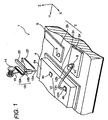
- Fig. 1 is a perspective view of a manner of connecting a wiring member such as a lead frame 2 to a semiconductor chip through a conductive wire 12.
- the semiconductor chip 4 is mounted on the lead frame 2.
- the lead frame 2 is arranged on a stage 6 of a bonding device 1.
- a wire spool 14 for the bonding device 1 houses a bonding wire used for bonding in a wound state.
- the bonding wire 16 when it is pulled out from the wire spool 14, is guided onto the stage 6 via a clamper 18 and a capillary 20.
- the bonding wire 16 passes between a pair of holding plates 18a and 18b.
- the bonding wire 16 further passes from the one end to the other end of a through-hole 20a.
- a ball 16a is formed in such a manner that the cut end is heated and molten using a discharge conductive member 22.
- the stage is movable in both X and Y directions in Fig. 1 in a state where the lead frame 2 and the semiconductor chip 4 are placed.
- the capillary 20 is movable in a Z direction.
- the lead frame 2 includes a plurality of inner leads 2a, 2b and an island 2c.
- the semiconductor chip 4 is connected to the island 2c of the lead frame 2 by silver paste.
- a semiconductor device (not shown) and bonding pads 4b and 4c are formed.
- lower conductive member 8 and 9 are formed, respectively.
- the conductive member pads 4b, 4c on the semiconductor chip are made of aluminum or aluminum alloy.
- the conductive member pads 4b, 4c are made of Au or Au alloy.
- the bonding wire 16 is a gold wire having a diameter of about 30 ⁇ m.
- a conductive wire 12 is composed of a ball conductive member 12a connected to the conductive member pad 4b, a connecting end 12b connected to the lower conductive member 8 on the lead frame and a connecting wire 12c which connects the ball conductive member 12a and the connecting end 12b.
- An upper conductive member 10 is provided on the connecting end 12b.
- an conductive member pad 4c is to be connected to an inner lead 2b.
- lower conductive members 8, 9 are formed of inner leads 2a, 2b.
- the lower conductive members 8, 9 can be formed of bumps such as a gold bump, copper bump and a solder bump, they are preferably formed in a convex shape which can be formed by melting the bonding wire 16 by discharge so as to be re-crystallized. In this way, the conductive member of a more soft material than the original wire material can be obtained. Since the lower conductive members 8,9 are formed by melting the wire having the diameter of about 30 ⁇ m to form the ball and bump, the diameter of the lower conductive members 8, 9 becomes several tens ⁇ m. The case where the wire is molten to form the lower conductive members 8, 9 will be explained below.
- the convex-shaped ball conductive member (Fig. 1) formed at the tip of the bonding wire 16 is fixed to the inner lead 2a.
- the crimping technique such as thermal crimping and ultrasonic thermal crimping is used.
- the bonding wire 16 held by the holding members 18a, 18b is cut at the edge of the through-hole 20a of the capillary 20.
- the lower conductive members 8, 9 are formed on the inner leads 2a, 2b.
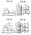
- Figs. 2A and 2B show the state after the above step has been completed.
- Fig. 2A is a side view and Fig. 2B is an top view.
- the lead frame 2 and the semiconductor chip 4 will be connected to each other by the bonding wire 16.
- the cut end of the bonding wire 16 held by the capillary (20 in Fig. 1) is molten by discharge to form a ball-shaped conductive member.
- the stage 6 is moved so that the ball-shaped conductive member is located on the bonding pad 4b of the semiconductor chip 4.
- the ball-shaped conductive member is crimped on the bonding pad 4b.
- the bonding wire 16 is moved without being cut while it is continuously unreeled so that the bonding tool 20 is located on the lower conductive member 8 formed on the inner lead 2a. After the bonding wire 16 has been bonded to the lower conductive member 8, it is cut.
- the bonding pad 4c is electrically connected to the lower conductive member 9.
- the bonding pads 4b, 4c of the semiconductor chip 4 are connected to the inner leads 2a, 2b, respectively.
- the conductive wire 12 contains a ball conductive member 12a on the pad 4b, a connecting end 12b and a conductive wire 12c connecting them to each other.
- the conductive wire 13 contains a ball conductive member 13a on the pad 4c, a connecting end 13b and a conductive wire 13c connecting them to each other.
- Figs. 3A and 3B show the lead frame 2 and semiconductor chip 4 after the above step has been executed.
- Fig. 3A is a side view and Fig. 3B is a top view.
- upper conductive members 10 and 11 are formed on the lower conductive members 8 and 9.
- the cut end of the bonding wire 16 held by the capillary 20 is molten by discharge to form a ball-shaped conductive member.
- the stage 6 is moved so that the ball-shaped conductive member is located on the lower conductive member 8 provided on the inner lead 2a.
- the connecting end 12 is crimped on the lower conductive member 8.
- the bonding wire 16 is cut.
- the upper conductive member 11 is provided on the lower conductive member 9.
- the connecting end 12b of the conductive wire 12 is sandwiched by the lower conductive member 8 and upper conductive member 9.
- the connecting end 13b of the conductive wire 13 is sandwiched by the lower conductive member 8 and upper conductive member 9 from its both sides.
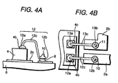
- Figs. 4A and 4B show the lead frame 2 and semiconductor chip 4 after the above step has been executed.
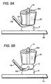
- Figs. 5A and 5B are enlarged views showing the manner of bonding the conductive wire 12 to the lower conductive member 8.
- Fig. 5A shows the manner of fixing the conductive wire 12 to the lower conductive member 8.
- the lower conductive member 8 has a diameter of about 100 ⁇ m for the wire having a diameter of 30 ⁇ m.
- weight is applied from above in bonding. Therefore, the edge of the capillary 20 will be brought into contact with the side of the conductive wire 12. Accordingly, the conductive wire 12 has a neck portion 12d.
- the connecting end 12b of the conductive wire 12 is sandwiched between the upper conductive member 10 and the lower conductive member 8. Since the upper conductive member 10 is formed to cover the neck portion 12d of the conductive wire 12 (the portion of the conductive wire 12 with which the edge of the capillary 20 is in contact) from above, the strength of the neck portion 12d is compensated for. In the embodiments described above, all of the lower conductive member 8, conductive wire 12 and upper conductive member 10 are made of the same kind of materials. The bonding strength among these three members is greater than that among different kinds of materials.
- the connecting end 12b of the conductive wire 12 is sandwiched by the upper conductive member 10 and lower conductive member 8 from its both sides. For this reason, the total bonding area of the conductive wire 12 is increased as compared with the case of provision of only the lower conductive member 8, thereby increasing the bonding strength.
- the lower conductive member 8 In fixing, since the lower conductive member 8 is deformed, the deformation of the conductive wire 12 itself can be suppressed. As a result, reduction of the sectional area in the neck portion 12d of the conductive wire 12 can be suppressed. This effect is particularly remarkable when the bonding wire 16 is recrystallized.
- the upper conductive member 10 is also formed by recrystallization of the bonding wire 16. Therefore, it is deformed in its bonding with the lower conductive member. Namely, its shape can be easily changed in accordance with the shape of the neck portion 12d so that the neck portion 12d can be protected.
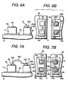
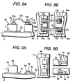
- Figs. 6A-8A an explanation will be given of another embodiment in which the wiring member is another semiconductor chip.
- Figs. 6A-8B correspond to Figs. 2A-4B, respectively.
- another semiconductor chip 24 is mounted on an island 2d.
- bonding pads 24b and 24c are formed on the main surface 24a of another semiconductor chip 24.
- bonding pads 24b and 24c are formed on these bonding pads 24b and 24c, the lower conductive member 8 and 9 are formed, respectively. Therefore, the explanation of Figs. 2A-4B can be applied to this mode except that the lower conductive members 8 and 9 are formed on the bonding pads 24b and 24c, not but on the inner leads 2a and 2c.
- This mode can also provide the same operation and effect as that when the present invention is applied to the wiring member of a lead frame 2.
- this connecting structure is provided, it is possible to realize the wire connection between chips by using the bonding pads having substantially same size.
- lower conductive members 8a, 9a are formed on inner leads 2a, 2b.
- the lower conductive members 8a, 9a are formed in a convex shape formed by melting the boding sire 16 by discharge so as to be re-crystallized as similar to the second embodiment.
- the ball conductive member (see, Fig. 1) formed at the tip of the bonding wire 16 is fixed to the inner lead 2a.
- the crimping technique such as thermal crimping and ultrasonic thermal crimping is used.
- the stage 6 is moved to the positions different from the lower conductive members 8a, 9a and the bonding wire 16 is fixed to the inner leads 2a and 2b.
- This fixing can be carried out without forming the ball, but may be carried out by forming the ball.
- the bonding wire 16 held by the holding members 18a, 18b is cut by the capillary 20.
- Each of the conductive wires thus formed is composed of a lower conductive member 8a, 9a, conductive portion 8c, 9c and a wire portion connecting them.
- the connecting portion 8c, 9c and the wire portion 8b, 9b are extended from the lower conductive member 8a, 9a. This permits the tension applied to the bonding portion to be dispersed.
- Figs. 9A and 9B show the state after the above step has been completed.
- Fig. 9A is a side view and Fig. 9B is an top view.
- the lead frame 2 and the semiconductor chip 4 will be connected to each other by the bonding wire 16.
- the cut end of the bonding wire 16 is molten by discharge to form a ball-shaped conductive member.
- the stage 6 is moved so that the ball-shaped conductive member is located on the bonding pad 4b of the semiconductor chip 4.
- the ball-shaped conductive member is crimped on the bonding pad 4b.
- the bonding wire 16 is moved without being cut while it is continuously unreeled so that the capillary 20 is located on the lower conductive member 8 formed on the inner lead 2a. After the bonding wire 16 has been fixed to the lower conductive member 8, the bonding wire 16 is cut.
- the bonding pad 4c is electrically connected to the inner lead 2b by the above crimping technique.
- the bonding pads 4b, 4c of the semiconductor chip 4 are connected to the inner leads 2a, 2b, respectively.
- the conductive wire 12 contains a ball conductive member 12a on the pad 4b, a connecting end 12b on the lower conductive member 8a and a conductive wire 12c connecting them to each other.
- the conductive wire 13 contains a ball conductive member 13a on the pad 4c, a connecting end 13b on the lower conductive member 9a and a conductive wire 13c connecting them to each other.
- Figs. 10A and 10B show the lead frame 2 and semiconductor chip 4 after the above step has been executed.
- Fig. 10A is a side view
- Fig. 10B is a top view.
- upper conductive members 10a and 11a is formed on the lower conductive members 8 and 9.
- the cut end of the bonding wire 16 is molten by discharge to form a ball-shaped conductive member.
- the stage 6 is moved so that the ball-shaped conductive member is located on the connecting end 2b of the conductive wire 12.
- the connecting end 12b is crimped on the lower conductive member 8a.
- the bonding wire 16 is fixed to the inner lead 2a at a different position from the lower conductive members 8a.
- the bonding can be carried out by the same technique as the crimping.
- the upper conductive member 11a is formed on the conducting end 13b of the conductive wire 13 and bonded to the inner lead 2b at the position 11c different from the lower conductive member 9a.
- the one connecting member contains the upper conductive member 10a, connecting portion 10c and wire portion 10b connecting them
- the other connecting member contains the upper conductive member 11a, connecting portion 11c and wire portion 11b connecting them.
- the connecting end 12b of the conductive wire 12 is sandwiched by the lower conductive member 8a and upper conductive member 10a from its both sides.
- the connecting end 13b of the conductive wire 13 is sandwiched by the lower conductive member 9a and upper conductive member 11a.
- Figs. 11A and 11B show the lead frame 2 and semiconductor chip 4 after the above step has been executed.
- Fig. 11A is a side view
- Fig. 11B is a top view.
- This embodiment can also provide the same operation and effect as the second embodiment. Namely, on the lower conductive member 8a, 9a and connecting end 12b, 13b, the upper conductive member 10a, 11a made of the same material as that of these members is provided. The fixing area of the connecting ends 12b, 13b of the conductive wires with the upper and lower conductive members is increased. Further, the upper conductive members 10a, 11a is formed to cover the connecting end 12b, 13b of the conductive wire 12, 13. Therefore, the upper conductive members 10a serves to protect the neck portion of the conductive wire 12, 13 from above. Such a structure can greatly improve the breaking strength against the tension applied to the conductive wire 12.
- an anchor structure in which the upper conductive member 10a (11a) and the connecting portion 10c (11c) formed integrally with it and the corresponding lower conductive member 8a (9a) and the connecting portion 8c (9c) formed integrally with it are fixed to the inner lead 2a (2b) at a plurality of positions.
- Such a structure permits the tension applied to the conductive wire 12, 13 to be dispersed at the plurality of fixing points.
- the anchor structure can be adopted in at least one of the lower conductive member and upper conductive member.
- the anchor structure prevents the electrical connection and mechanical bonding from being lost completely.
- the method according to the invention can be applied to the semiconductor chip 4, 24 having at least one of the a light receiving element and a light emitting element, or any other active elements.
- the semiconductor chip 4, 24 in which the electrical connection to the conductive wire has been completed can be sealed together with the lead frame 2 using mold resin. Further, the semiconductor chips 4 and 24 are integrally or individually sealed by mold resin.
- the semiconductor chip 4, 24 is electrically connected to the wiring member so that the neck portion 12d is protected by the upper conductive member 10, it is sealed using the mold resin.
- the resin for sealing the light receiving and light emitting elements the resin should be permeable to the light having a wavelength in which these elements has sensitivity. Therefore, the stress relaxation agent which relaxes the stress of the mold resin can not be added to the resin.
- the semiconductor device according to the invention can be effectively applied to such a case.
- Fig. 13 shows the result of the breakage strength test executed for the semiconductor device shown in Figs. 4A and 4B according to the mode for carrying out the invention.
- the abscissa indicates the breakage strength of the neck portion in gram (g), and the ordinate indicates its occurring frequency in a relative value.
- three remarkable peaks A, B and C appear. Peak A is located at the position of the breakage strength of about 15 g which corresponds to the data relative to the conventional structure in which both lower conductive member and upper conductive member are not provided. Peak B is located at the position of the breakage strength of about 25g which corresponds to the structure in which the upper conductive member is not provided.
- Peak C is located at the position of the breakage strength of about 33g which corresponds to the structure according to the invention in which both lower and upper conductive members are provided. In the order of the peak A - peak C, the dispersion is decreased. Thus, it has been verified that the structure corresponding to the peak C exhibits not only a great strength but also stabilized characteristic.
- the thickness of the lower conductive member is preferably 10 ⁇ or more in the modes for carrying out the invention.
- Fig. 14 is a characteristic view with the thickness d of the lower conductive member in abscissa and the wire-pull-strength indicative of a wire pulling strength in ordinate.
- the thickness d of the lower conductive member denotes the value when it is connected to the conductive wire.
- the present invention is clearly different from the technology disclosed in JP-A-55-118643.
- ball bond and stitch bond are made on the Al surface using a bonding wire.
- the bonding wire is once connected to the ball bond formed on the Al surface and thereafter extended to the stitch bond. Therefore, the bonding wire has no connecting end. No conductive member is formed on the ball band. Therefore, the electric connecting area between the bonding wire and ball bond is small and bonding area is also small.
- the connecting portion of the conductive wire to be connected to the wiring member is sandwiched between the upper and lower conductive members. Therefore, the neck portion of the conductive wire can be protected by the upper conductive member so that the neck portion can be reinforced.
- the total bonding area of the conductive wire is increased as compared with the case of the provision of only the lower conductive member, and hence the bonding strength is increased.
- the lower conductive member is formed on the lower side of the connecting portion of the conductive wire, the lower conductive member is deformed. Therefore, the deformation of the conductive wire itself is suppressed. Thus, reduction in the sectional area of the neck portion of the conductive wire can also be suppressed.
- the lower conductive member is provided before the conductive wire is connected to the wiring member. Therefore, it can provide a conductive portion capable of absorbing the stress applied in bonding at the portion to which the conductive wire is to be fixed. Therefore, the deformation of the conductive wire can be suppressed. Further, since the upper conductive member is provided on the lower conductive member through the conductive wire after the conductive wire has been connected to the lower conductive member, the neck portion of the conductive wire formed when the conductive wire is connected to the lower conductive member can be protected by the upper conductive member.
- a semiconductor device capable of reducing breakage of a bonding wire and a method of manufacturing it can be provided.
Landscapes
- Wire Bonding (AREA)
Applications Claiming Priority (2)
| Application Number | Priority Date | Filing Date | Title |
|---|---|---|---|
| JP11181948A JP2001015541A (ja) | 1999-06-28 | 1999-06-28 | 半導体装置および半導体装置の製造方法 |
| JP18194899 | 1999-06-28 |
Publications (1)
| Publication Number | Publication Date |
|---|---|
| EP1065712A1 true EP1065712A1 (fr) | 2001-01-03 |
Family
ID=16109687
Family Applications (1)
| Application Number | Title | Priority Date | Filing Date |
|---|---|---|---|
| EP00113595A Ceased EP1065712A1 (fr) | 1999-06-28 | 2000-06-27 | Méthode de soudure de fil dans un dispositif semiconducteur |
Country Status (3)
| Country | Link |
|---|---|
| US (2) | US6426563B1 (fr) |
| EP (1) | EP1065712A1 (fr) |
| JP (1) | JP2001015541A (fr) |
Cited By (2)
| Publication number | Priority date | Publication date | Assignee | Title |
|---|---|---|---|---|
| US7268010B2 (en) | 2004-10-08 | 2007-09-11 | Kingbright Electronic Co., Ltd. | Method of manufacturing an LED |
| EP2947684A4 (fr) * | 2013-01-18 | 2016-10-05 | Hamamatsu Photonics Kk | Dispositif à composants électroniques |
Families Citing this family (18)
| Publication number | Priority date | Publication date | Assignee | Title |
|---|---|---|---|---|
| JP2002280414A (ja) * | 2001-03-22 | 2002-09-27 | Mitsubishi Electric Corp | 半導体装置およびその製造方法 |
| US6854637B2 (en) * | 2003-02-20 | 2005-02-15 | Freescale Semiconductor, Inc. | Wirebonding insulated wire |
| US7408119B2 (en) * | 2003-10-15 | 2008-08-05 | Agilent Technologies, Inc. | Electrical interconnection for high-frequency devices |
| US7214606B2 (en) * | 2004-03-11 | 2007-05-08 | Asm Technology Singapore Pte Ltd. | Method of fabricating a wire bond with multiple stitch bonds |
| JP4091562B2 (ja) * | 2004-03-29 | 2008-05-28 | ファナック株式会社 | モータ駆動装置 |
| WO2006018671A1 (fr) * | 2004-08-19 | 2006-02-23 | Infineon Technologies Ag | Boitier a grilles de connexion a semi-conducteurs et a fils mixtes |
| JP4266369B2 (ja) * | 2005-02-24 | 2009-05-20 | 株式会社新川 | ワイヤボンディング方法 |
| JP5008832B2 (ja) * | 2005-04-15 | 2012-08-22 | ローム株式会社 | 半導体装置及び半導体装置の製造方法 |
| JP2006324553A (ja) | 2005-05-20 | 2006-11-30 | Renesas Technology Corp | 半導体装置及びその製造方法 |
| JP2007134486A (ja) * | 2005-11-10 | 2007-05-31 | Toshiba Corp | 積層型半導体装置及びその製造方法 |
| CN102412167B (zh) * | 2010-09-25 | 2016-02-03 | 飞思卡尔半导体公司 | 用于线接合的固定 |
| KR101805118B1 (ko) * | 2011-05-30 | 2017-12-05 | 엘지이노텍 주식회사 | 발광소자패키지 |
| MY181180A (en) | 2011-09-09 | 2020-12-21 | Carsem M Sdn Bhd | Low loop wire bonding |
| US20140091465A1 (en) * | 2012-09-28 | 2014-04-03 | Texas Instruments Incorporated | Leadframe having sloped metal terminals for wirebonding |
| US9368435B2 (en) | 2014-09-23 | 2016-06-14 | Infineon Technologies Ag | Electronic component |
| JP6680239B2 (ja) * | 2017-02-20 | 2020-04-15 | 日亜化学工業株式会社 | 発光装置の製造方法 |
| WO2022219995A1 (fr) * | 2021-04-12 | 2022-10-20 | ローム株式会社 | Dispositif à semi-conducteurs |
| CN114050136A (zh) * | 2021-10-28 | 2022-02-15 | 西安微电子技术研究所 | 一种芯片焊盘植球整平及二次焊接的方法 |
Citations (4)
| Publication number | Priority date | Publication date | Assignee | Title |
|---|---|---|---|---|
| JPH01158742A (ja) * | 1987-12-16 | 1989-06-21 | Sanken Electric Co Ltd | リード細線を有する装置の製造方法 |
| JPH02114545A (ja) * | 1988-10-24 | 1990-04-26 | Toshiba Corp | ワイヤボンディング接続方法 |
| JPH08340019A (ja) * | 1995-06-13 | 1996-12-24 | Matsushita Electric Ind Co Ltd | 基板、基板の製造方法及びワイヤボンディング方法 |
| DE19744266A1 (de) * | 1996-10-07 | 1998-04-16 | Denso Corp | Drahtbondierungsverfahren |
Family Cites Families (10)
| Publication number | Priority date | Publication date | Assignee | Title |
|---|---|---|---|---|
| US4067039A (en) * | 1975-03-17 | 1978-01-03 | Motorola, Inc. | Ultrasonic bonding head |
| JPS55118643A (en) | 1979-03-06 | 1980-09-11 | Toshiba Corp | Wire bonding process |
| US4845543A (en) * | 1983-09-28 | 1989-07-04 | Hitachi, Ltd. | Semiconductor device and method of manufacturing the same |
| JPH0249447A (ja) * | 1988-05-20 | 1990-02-19 | Hitachi Ltd | 半導体装置とその製造方法 |
| US5291061A (en) * | 1993-04-06 | 1994-03-01 | Micron Semiconductor, Inc. | Multi-chip stacked devices |
| WO1998021780A2 (fr) | 1996-11-11 | 1998-05-22 | Siemens Aktiengesellschaft | Connexion entre deux surfaces de contact et procede permettant de realiser une connexion de ce type |
| DE19703639A1 (de) * | 1997-01-31 | 1998-08-06 | Bosch Gmbh Robert | Verfahren zur Herstellung von Bonddrahtverbindungen |
| US6180891B1 (en) * | 1997-02-26 | 2001-01-30 | International Business Machines Corporation | Control of size and heat affected zone for fine pitch wire bonding |
| US5976964A (en) * | 1997-04-22 | 1999-11-02 | Micron Technology, Inc. | Method of improving interconnect of semiconductor device by utilizing a flattened ball bond |
| US6296789B1 (en) * | 1998-02-20 | 2001-10-02 | Sumitomo Electric Industries, Ltd. | Optical module and a method of fabricating the same |
-
1999
- 1999-06-28 JP JP11181948A patent/JP2001015541A/ja active Pending
-
2000
- 2000-06-27 EP EP00113595A patent/EP1065712A1/fr not_active Ceased
- 2000-06-28 US US09/604,802 patent/US6426563B1/en not_active Expired - Fee Related
-
2002
- 2002-05-09 US US10/141,179 patent/US6784090B2/en not_active Expired - Fee Related
Patent Citations (4)
| Publication number | Priority date | Publication date | Assignee | Title |
|---|---|---|---|---|
| JPH01158742A (ja) * | 1987-12-16 | 1989-06-21 | Sanken Electric Co Ltd | リード細線を有する装置の製造方法 |
| JPH02114545A (ja) * | 1988-10-24 | 1990-04-26 | Toshiba Corp | ワイヤボンディング接続方法 |
| JPH08340019A (ja) * | 1995-06-13 | 1996-12-24 | Matsushita Electric Ind Co Ltd | 基板、基板の製造方法及びワイヤボンディング方法 |
| DE19744266A1 (de) * | 1996-10-07 | 1998-04-16 | Denso Corp | Drahtbondierungsverfahren |
Non-Patent Citations (3)
| Title |
|---|
| PATENT ABSTRACTS OF JAPAN vol. 013, no. 429 (E - 823) 25 September 1989 (1989-09-25) * |
| PATENT ABSTRACTS OF JAPAN vol. 014, no. 338 (E - 0954) 20 July 1990 (1990-07-20) * |
| PATENT ABSTRACTS OF JAPAN vol. 1997, no. 04 30 April 1997 (1997-04-30) * |
Cited By (3)
| Publication number | Priority date | Publication date | Assignee | Title |
|---|---|---|---|---|
| US7268010B2 (en) | 2004-10-08 | 2007-09-11 | Kingbright Electronic Co., Ltd. | Method of manufacturing an LED |
| EP2947684A4 (fr) * | 2013-01-18 | 2016-10-05 | Hamamatsu Photonics Kk | Dispositif à composants électroniques |
| US9502456B2 (en) | 2013-01-18 | 2016-11-22 | Hamamatsu Photonics K.K. | Electronic component device |
Also Published As
| Publication number | Publication date |
|---|---|
| JP2001015541A (ja) | 2001-01-19 |
| US20020171155A1 (en) | 2002-11-21 |
| US6426563B1 (en) | 2002-07-30 |
| US6784090B2 (en) | 2004-08-31 |
Similar Documents
| Publication | Publication Date | Title |
|---|---|---|
| US6784090B2 (en) | Semiconductor device and method for manufacturing the same | |
| US6764880B2 (en) | Semiconductor package and fabricating method thereof | |
| US5770888A (en) | Integrated chip package with reduced dimensions and leads exposed from the top and bottom of the package | |
| US6222258B1 (en) | Semiconductor device and method for producing a semiconductor device | |
| US9087827B2 (en) | Mixed wire semiconductor lead frame package | |
| US6762079B2 (en) | Methods for fabricating dual loc semiconductor die assembly employing floating lead finger structure | |
| US20020030289A1 (en) | Wire arrayed chip size package and fabrication method thereof | |
| US20090174054A1 (en) | Module with Flat Construction and Method for Placing Components | |
| US8759987B2 (en) | Semiconductor device and method of manufacturing the semiconductor device | |
| KR100817076B1 (ko) | 와이어 본딩용으로 부분적으로 절연 피복된 금속 와이어 및이를 이용한 반도체 패키지의 와이어 본딩 방법 | |
| US20170084569A1 (en) | Semiconductor device and production method therefor | |
| CN1946504A (zh) | 低回路导线邦定的系统和方法 | |
| US6774479B2 (en) | Electronic device having a semiconductor chip on a semiconductor chip connection plate and a method for producing the electronic device | |
| US8012869B2 (en) | Bonded structure and bonding method | |
| US8258611B2 (en) | Leadframe structure for electronic packages | |
| JPH04155854A (ja) | 半導体集積回路装置およびそれに用いるリードフレーム | |
| EP4535421A1 (fr) | Dispositif semi-conducteur encapsulé et son procédé de fabrication | |
| EP4517819A1 (fr) | Procédé de fabrication de dispositifs semi-conducteurs, composant correspondant et dispositif semi-conducteur | |
| JP3923379B2 (ja) | 半導体装置 | |
| JP3229816B2 (ja) | 樹脂封止型半導体装置の製造方法 | |
| JP2000012621A (ja) | 半導体装置およびその製造方法 | |
| EP1381084A1 (fr) | Dispositif semi-conducteur et procédé de fabrication | |
| JP2002057244A (ja) | 半導体装置およびその製造方法 | |
| JP2002016210A (ja) | 半導体装置 | |
| KR100355639B1 (ko) | 수지봉지형 반도체소자 및 그를 이용한 반도체장치의 제조방법 |
Legal Events
| Date | Code | Title | Description |
|---|---|---|---|
| PUAI | Public reference made under article 153(3) epc to a published international application that has entered the european phase |
Free format text: ORIGINAL CODE: 0009012 |
|
| AK | Designated contracting states |
Kind code of ref document: A1 Designated state(s): DE FR GB IT |
|
| AX | Request for extension of the european patent |
Free format text: AL;LT;LV;MK;RO;SI |
|
| 17P | Request for examination filed |
Effective date: 20010305 |
|
| 17Q | First examination report despatched |
Effective date: 20010412 |
|
| AKX | Designation fees paid |
Free format text: DE FR GB IT |
|
| STAA | Information on the status of an ep patent application or granted ep patent |
Free format text: STATUS: THE APPLICATION HAS BEEN REFUSED |
|
| 18R | Application refused |
Effective date: 20020325 |