EP1067404A1 - Positronenemissions-Tomographie - Google Patents
Positronenemissions-Tomographie Download PDFInfo
- Publication number
- EP1067404A1 EP1067404A1 EP00401907A EP00401907A EP1067404A1 EP 1067404 A1 EP1067404 A1 EP 1067404A1 EP 00401907 A EP00401907 A EP 00401907A EP 00401907 A EP00401907 A EP 00401907A EP 1067404 A1 EP1067404 A1 EP 1067404A1
- Authority
- EP
- European Patent Office
- Prior art keywords
- electrodes
- electronic circuit
- detectors
- detection device
- detector
- Prior art date
- Legal status (The legal status is an assumption and is not a legal conclusion. Google has not performed a legal analysis and makes no representation as to the accuracy of the status listed.)
- Withdrawn
Links
- 238000002600 positron emission tomography Methods 0.000 title description 2
- 238000001514 detection method Methods 0.000 claims abstract description 23
- 239000004065 semiconductor Substances 0.000 claims abstract description 17
- 238000000034 method Methods 0.000 claims abstract description 12
- 229910004611 CdZnTe Inorganic materials 0.000 claims abstract description 7
- 230000005684 electric field Effects 0.000 claims abstract description 7
- 239000000463 material Substances 0.000 claims abstract description 7
- 239000013078 crystal Substances 0.000 claims abstract description 6
- 230000008569 process Effects 0.000 claims description 7
- 239000003990 capacitor Substances 0.000 claims description 4
- 239000002800 charge carrier Substances 0.000 description 6
- 238000005259 measurement Methods 0.000 description 5
- 210000000056 organ Anatomy 0.000 description 5
- MARUHZGHZWCEQU-UHFFFAOYSA-N 5-phenyl-2h-tetrazole Chemical compound C1=CC=CC=C1C1=NNN=N1 MARUHZGHZWCEQU-UHFFFAOYSA-N 0.000 description 4
- 238000006243 chemical reaction Methods 0.000 description 4
- 238000010586 diagram Methods 0.000 description 3
- 230000005012 migration Effects 0.000 description 3
- 238000013508 migration Methods 0.000 description 3
- IJGRMHOSHXDMSA-UHFFFAOYSA-N Atomic nitrogen Chemical compound N#N IJGRMHOSHXDMSA-UHFFFAOYSA-N 0.000 description 2
- 229910004613 CdTe Inorganic materials 0.000 description 2
- 229910052793 cadmium Inorganic materials 0.000 description 2
- -1 cadmium tellurides Chemical class 0.000 description 2
- 238000009206 nuclear medicine Methods 0.000 description 2
- 239000000700 radioactive tracer Substances 0.000 description 2
- 230000004044 response Effects 0.000 description 2
- 238000003325 tomography Methods 0.000 description 2
- OKTJSMMVPCPJKN-UHFFFAOYSA-N Carbon Chemical compound [C] OKTJSMMVPCPJKN-UHFFFAOYSA-N 0.000 description 1
- PXGOKWXKJXAPGV-UHFFFAOYSA-N Fluorine Chemical compound FF PXGOKWXKJXAPGV-UHFFFAOYSA-N 0.000 description 1
- 238000010521 absorption reaction Methods 0.000 description 1
- 230000001133 acceleration Effects 0.000 description 1
- 230000003321 amplification Effects 0.000 description 1
- QVGXLLKOCUKJST-UHFFFAOYSA-N atomic oxygen Chemical compound [O] QVGXLLKOCUKJST-UHFFFAOYSA-N 0.000 description 1
- 230000008901 benefit Effects 0.000 description 1
- 229910052799 carbon Inorganic materials 0.000 description 1
- 239000000969 carrier Substances 0.000 description 1
- 238000002109 crystal growth method Methods 0.000 description 1
- 238000002425 crystallisation Methods 0.000 description 1
- 230000008025 crystallization Effects 0.000 description 1
- 238000009795 derivation Methods 0.000 description 1
- 238000000295 emission spectrum Methods 0.000 description 1
- 230000002349 favourable effect Effects 0.000 description 1
- 229910052731 fluorine Inorganic materials 0.000 description 1
- 239000011737 fluorine Substances 0.000 description 1
- 230000004313 glare Effects 0.000 description 1
- 230000006698 induction Effects 0.000 description 1
- 230000010354 integration Effects 0.000 description 1
- 230000003993 interaction Effects 0.000 description 1
- 230000004807 localization Effects 0.000 description 1
- 229910052757 nitrogen Inorganic materials 0.000 description 1
- 238000003199 nucleic acid amplification method Methods 0.000 description 1
- 229910052760 oxygen Inorganic materials 0.000 description 1
- 239000001301 oxygen Substances 0.000 description 1
- 230000001681 protective effect Effects 0.000 description 1
- 230000002285 radioactive effect Effects 0.000 description 1
- 230000000717 retained effect Effects 0.000 description 1
- 230000035945 sensitivity Effects 0.000 description 1
- 238000007493 shaping process Methods 0.000 description 1
- 230000007847 structural defect Effects 0.000 description 1
- 230000002123 temporal effect Effects 0.000 description 1
Images


Classifications
-
- G—PHYSICS
- G01—MEASURING; TESTING
- G01T—MEASUREMENT OF NUCLEAR OR X-RADIATION
- G01T1/00—Measuring X-radiation, gamma radiation, corpuscular radiation, or cosmic radiation
- G01T1/29—Measurement performed on radiation beams, e.g. position or section of the beam; Measurement of spatial distribution of radiation
- G01T1/2914—Measurement of spatial distribution of radiation
- G01T1/2985—In depth localisation, e.g. using positron emitters; Tomographic imaging (longitudinal and transverse section imaging; apparatus for radiation diagnosis sequentially in different planes, steroscopic radiation diagnosis)
Definitions
- the performance of a detector is determined on the one hand by its ability to absorb the maximum photons of the desired energy and secondly by the speed at which it will give this information, that is, its response time.
- This second criterion is fundamental in the PET process: when one of the two detector networks detects a photon, we measure during a window very short time, from 5 to 10 nanoseconds to maximum, the absorption of the associated photon coming from the same annihilation on the opposite detector network. During this time window, emissions fortuitous events, arising from other causes, may be detected on other detectors of this second network and give incorrect information about the origin of the annihilation of the positron, because the line connecting the two events recorded and assigned to annihilation then passes away from its place. More the shorter the detection time window, the shorter the proportion of incidental emission detection is reduced and the more the spatial resolution of the image will be high.
- Detector thickness and more precisely from the part where the photons are converted is an important parameter of the response time, because a small thickness governs a short answer, the light crossing faster detector; however, a thickness must be maintained sufficient to secure a suitable share of photons.
- scintillator detectors offer a short answer they are less satisfactory for the level of the signal they produce and for them glare phenomena that limit the number of shots accepted by the camera and thus give a low sensitivity. That's why we start to take an interest in semiconductor-based detectors like cadmium tellurides (CdZnTe, CdTe, CdTe doped, ...), which allow direct detection of photons by converting them into charge carriers electric, in number much higher than that which is obtained in indirect detection, which increases the signal got.
- the collection of charge carriers is made with simplicity by deposited electrodes on the semiconductor, to which we apply a bias voltage which creates an electric field in the semiconductor, favoring the migration of charge carriers to the electrodes.
- Signal amplification and shaping are then carried out by an electronic circuit integrated into each detector and more compact than in the solution to scintillator and photo-multiplier.
- the invention is based on a new detection method, which significantly improves the performance of direct semiconductor detection and therefore should make it more attractive.
- the basic idea is to replace the charge preamplifier, natural use to detect discrete events like arrival individual photons, by a preamplifier current, the essential property of which is that it is devoid of capacitor and therefore does not delay the measurement by performing time integration.
- the acceleration of the measurement due to the preamplifier current is compensated by a loss of the accuracy of measure, which however is not harmful in the case of a PET tomography process where the photons are similar and where the measures are counts rather that level measurements.
- the signal ratio on the noise is also worse than with a preamplifier charge, but it remains acceptable, and the noise of the detector can be made very weak by new so-called high crystal growth methods pressure, like the HPBM process (High Pressure Bridgman Method), which improve its resistivity, in particular that of CdZnTe.
- HPBM process High Pressure Bridgman Method
- the resistivity increases, it is then possible to increase the voltage applied to material electrodes.
- a first consequence is the decrease in signal duration, i.e. time of charge migration to the electrodes: the detector dead time is shorter.
- a second consequence is the increase in the peak signal, this which gives a better signal to noise ratio.
- a another favorable aspect of the invention consists in fully integrate electronics in ASIC form ("Application Specific Integrated Circuit") in order to remove certain stray capacities, such as length of the connection between the detectors and the preamplifier, and thus improve very clearly the speed of electronic measurement.
- ASIC form Application Specific Integrated Circuit
- Use of a high resistivity semiconductor also reduces the connection capacity between the detector and the current preamplifier.
- Another idea we can apply consists in having a signal discriminator, according to an established threshold, with a constant fraction of time up to a signal peak, in the electronic circuit.
- the invention relates under its most generally forms a detection device for a positron emission tomograph, comprising a pair of opposite networks of detectors, networks of detectors including detection cells composed of a block of semiconductor material where the photons are converted into electrical charges, electrodes for creating an electric field in the block, and an electronic circuit connecting the electrodes to a current meter, characterized in that the electronic circuit includes a current preamplifier, devoid of capacitor.
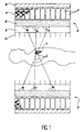
- FIG 1 there is shown a section subject to examination of a human body including an organ 1 loaded with radioactive tracer emits positrons. Each pair of photons emitted by a positron which is annihilated travels a straight line 2 susceptible result in a pair of detector networks 3 located on either side of organ 1.
- detector networks 3 located on either side of organ 1.
- We have shown here classic 3 networks comprising from front to back a collimator 4, a layer of scintillator 5, a light guide 6 and photomultiplier tubes 7 which lead to an electronic measurement circuit 8.
- FIG. 2 shows a semiconductor detector proposed in the prior art, where the crystal of cadmium telluride (CdZnTe) is a block rectangular 10 with two side faces opposite are covered with electrodes 11 creating a field electric transverse, perpendicular to the direction 12. The whole is embedded in a protective cover 13 at the rear of which finds a collector 14 and a preamplifier charge 15.
- CdZnTe crystal of cadmium telluride
- Figure 3 illustrates a preamplifier current 20 whose input terminal 21 collects a current supplied by a device 22 and whose terminal output 23 emits the amplified current. Its elements essential are a subtractor circuit 24 whose positive terminal is connected to earth, the negative terminal at the input terminal 21 and the output at terminal 23; and a resistor 25 in derivation of the subtractor circuit 24 between terminals 21 and 23.
- This preamplifier does not includes no capacitor, and we saw that it was advantageous to eliminate or reduce all links capacitive that could be between the preamplifier 20 and device 22.
- FIG. 4 is an illustrative diagram of the detectors of the invention.
- the ⁇ photons emitted from a ⁇ positron reach two detectors 30 belonging to opposite networks (such as networks 3) which each include a block 31 of cadmium telluride crystal (CdZnTe) having grown under pressure to give it a high resistivity, of the order of 10 10 ⁇ cm or more.
- Electrodes 32 are arranged at the ends of the block 31 to create an electric field in the irradiation direction, and the current preamplifier 20 is adjacent to the block 31 and is electrically connected to it.
- the output terminal 23 of the preamplifier 20 is connected to a discriminator 33; the discriminators 33 of the various detectors 30 are connected to an amplitude-time converter 34 and then to a multi-channel analyzer 35 which gives the emission spectrum as a function of time.
- a delay device 36 is arranged behind the detectors 30 of one of the networks of the pair, so that the signals consecutive to the same annihilation do not arrive at the same time at the converter 34 and do not saturate the logic.
- the blocks 31 are 12 to 15 mm deep, and their transverse dimensions are not critical.
- the usefulness of the discriminator 33 could be understood using Figure 5 which illustrates the current produced by a photon arriving on a detector 30 as a function of time: these curves have a fairly long plateau preceded by rapid growth at from zero.
- the time window usable is so narrow that one cannot measure the signal that during this transitional period amplitude increase.
- the line curve full 40 illustrates the amplitude obtained for a photon which has retained its energy, and the dotted curve 41 that of a photon that arrived with energy lower in crystal 31, for example by a interaction with an atom of the patient's body, what we will observe very often.
- the devices usual discrimination operate with a threshold 42 fixed: the time t1 that the curve 40 takes to reach it is much lower than that t2 that the curve 41 puts.
Landscapes
- Physics & Mathematics (AREA)
- Health & Medical Sciences (AREA)
- Life Sciences & Earth Sciences (AREA)
- General Physics & Mathematics (AREA)
- High Energy & Nuclear Physics (AREA)
- Molecular Biology (AREA)
- Spectroscopy & Molecular Physics (AREA)
- Measurement Of Radiation (AREA)
- Nuclear Medicine (AREA)
Applications Claiming Priority (2)
| Application Number | Priority Date | Filing Date | Title |
|---|---|---|---|
| FR9908859 | 1999-07-08 | ||
| FR9908859A FR2796160B1 (fr) | 1999-07-08 | 1999-07-08 | Dispositif de detection pour un tomographe a emission de positrons |
Publications (1)
| Publication Number | Publication Date |
|---|---|
| EP1067404A1 true EP1067404A1 (de) | 2001-01-10 |
Family
ID=9547875
Family Applications (1)
| Application Number | Title | Priority Date | Filing Date |
|---|---|---|---|
| EP00401907A Withdrawn EP1067404A1 (de) | 1999-07-08 | 2000-07-04 | Positronenemissions-Tomographie |
Country Status (2)
| Country | Link |
|---|---|
| EP (1) | EP1067404A1 (de) |
| FR (1) | FR2796160B1 (de) |
Cited By (1)
| Publication number | Priority date | Publication date | Assignee | Title |
|---|---|---|---|---|
| CN106547015A (zh) * | 2016-10-28 | 2017-03-29 | 中国计量科学研究院 | 探测器 |
-
1999
- 1999-07-08 FR FR9908859A patent/FR2796160B1/fr not_active Expired - Fee Related
-
2000
- 2000-07-04 EP EP00401907A patent/EP1067404A1/de not_active Withdrawn
Non-Patent Citations (3)
| Title |
|---|
| EISEN Y ET AL: "CdTe and CdZnTe gamma ray detectors for medical and industrial imaging systems", NUCLEAR INSTRUMENTS & METHODS IN PHYSICS RESEARCH, SECTION - A: ACCELERATORS, SPECTROMETERS, DETECTORS AND ASSOCIATED EQUIPMENT,NL,NORTH-HOLLAND PUBLISHING COMPANY. AMSTERDAM, vol. 428, no. 1, 1 June 1999 (1999-06-01), pages 158 - 170, XP004169929, ISSN: 0168-9002 * |
| IWATA,K ET AL: "Improvements in CdZnTe Detection System for Combined X-ray CT and SPECT", 1998 IEEE NUCLEAR SCIENCE SYMPOSIUM CONFERENCE RECORD, vol. 2, 8 November 1998 (1998-11-08) - 14 November 1998 (1998-11-14), Toronto,Canada, pages 747 - 753, XP002133056 * |
| PICHLER, B J ET AL.: "Feasibility Study of a Compact High Resolution dcual Layer LSO_APD Detector Module for PET", 1988 IEEE NUCLEAR SCIENCE SYMPOSIUM RECORD, vol. 2, 8 November 1998 (1998-11-08) - 14 November 1998 (1998-11-14), Toronto, canada, pages 1199 - 1203, XP002133057 * |
Cited By (1)
| Publication number | Priority date | Publication date | Assignee | Title |
|---|---|---|---|---|
| CN106547015A (zh) * | 2016-10-28 | 2017-03-29 | 中国计量科学研究院 | 探测器 |
Also Published As
| Publication number | Publication date |
|---|---|
| FR2796160A1 (fr) | 2001-01-12 |
| FR2796160B1 (fr) | 2001-08-17 |
Similar Documents
| Publication | Publication Date | Title |
|---|---|---|
| EP0763751B1 (de) | Verfahren und Vorrichtung zur Korrektur von Signalen in der Gammaphotonenspektroskopie | |
| Powolny et al. | Time-based readout of a silicon photomultiplier (SiPM) for time of flight positron emission tomography (TOF-PET) | |
| CN105339810B (zh) | 半导体闪烁探测器 | |
| EP2507652B1 (de) | Verfahren zur kalibrierung eines röntgendetektors | |
| WO1998016851A1 (fr) | Dispositif et procede de collection et de codage de signaux issus de photodetecteurs | |
| EP1004040B1 (de) | Vorrichtung zur spektrometrischen messung im gebiet der detektion von gammaphotonen | |
| Derenzo et al. | Initial characterization of a position-sensitive photodiode/BGO detector for PET | |
| Veale et al. | Cadmium zinc telluride pixel detectors for high-intensity x-ray imaging at free electron lasers | |
| EP0851512A1 (de) | Halbleiterstrahlungsdetektor mit hohem Widerstand für ionisierende Strahlung | |
| EP1037070B1 (de) | Verfahren und Vorrichtung zur Klassifizierung von Ereignissen eines Gammastrahlungsdetektors in Echtzeit | |
| Liu et al. | Performance study of Philips digital silicon photomultiplier coupled to scintillating crystals | |
| EP0907086B1 (de) | Vorrichtung zum Messen der Aufsteigszeit von verrauschten Signalen von Gamma- oder Röntgendetektoren | |
| US6011264A (en) | Apparatus, system and method for gamma ray and x-ray detection | |
| EP1067404A1 (de) | Positronenemissions-Tomographie | |
| Rossignol et al. | A 3D photon-to-digital converter readout for low-power and large-area applications | |
| EP0620451A1 (de) | Teilchen-Dosimeter | |
| Murayama | A simple timing discriminator for a BGO scintillation detector | |
| Philippov et al. | Digital signal processing for SiPM timing resolution | |
| FR2497356A1 (fr) | Camera a scintillation | |
| Fu et al. | Recovery of inter-crystal compton scattering events for sensitivity improvement of sub-250 ps TOF-PET detector | |
| Visser et al. | Development of low power high speed readout electronics for high resolution PET with LSO and APD arrays | |
| EP0775322B1 (de) | System und methode zum nachweis von ionisierender strahlung | |
| EP1058128A1 (de) | Verfahren und Vorrichtung zur Unterscheidung von Impulsen von Halbleiter-Strahlungsdetektoren | |
| Derenzo et al. | Initial characterization of a position-sensitive photodiode/BGO detector for PET | |
| Frach et al. | Assessment of photodiodes as a light detector for PET scanners |
Legal Events
| Date | Code | Title | Description |
|---|---|---|---|
| PUAI | Public reference made under article 153(3) epc to a published international application that has entered the european phase |
Free format text: ORIGINAL CODE: 0009012 |
|
| AK | Designated contracting states |
Kind code of ref document: A1 Designated state(s): DE GB IT |
|
| AX | Request for extension of the european patent |
Free format text: AL;LT;LV;MK;RO;SI |
|
| 17P | Request for examination filed |
Effective date: 20010630 |
|
| AKX | Designation fees paid |
Free format text: DE GB IT |
|
| STAA | Information on the status of an ep patent application or granted ep patent |
Free format text: STATUS: THE APPLICATION IS DEEMED TO BE WITHDRAWN |
|
| 18D | Application deemed to be withdrawn |
Effective date: 20060201 |