EP1067569A1 - Dispositif mécanique de commutation rapide - Google Patents
Dispositif mécanique de commutation rapide Download PDFInfo
- Publication number
- EP1067569A1 EP1067569A1 EP99810596A EP99810596A EP1067569A1 EP 1067569 A1 EP1067569 A1 EP 1067569A1 EP 99810596 A EP99810596 A EP 99810596A EP 99810596 A EP99810596 A EP 99810596A EP 1067569 A1 EP1067569 A1 EP 1067569A1
- Authority
- EP
- European Patent Office
- Prior art keywords
- switching point
- point according
- coils
- switching
- contact
- Prior art date
- Legal status (The legal status is an assumption and is not a legal conclusion. Google has not performed a legal analysis and makes no representation as to the accuracy of the status listed.)
- Granted
Links
- 239000003990 capacitor Substances 0.000 description 15
- 238000000034 method Methods 0.000 description 11
- 230000005520 electrodynamics Effects 0.000 description 5
- 230000000694 effects Effects 0.000 description 4
- 230000015572 biosynthetic process Effects 0.000 description 2
- 238000010304 firing Methods 0.000 description 2
- 230000006698 induction Effects 0.000 description 2
- XAGFODPZIPBFFR-UHFFFAOYSA-N aluminium Chemical compound [Al] XAGFODPZIPBFFR-UHFFFAOYSA-N 0.000 description 1
- 229910052782 aluminium Inorganic materials 0.000 description 1
- 230000005540 biological transmission Effects 0.000 description 1
- 230000003111 delayed effect Effects 0.000 description 1
- 238000004146 energy storage Methods 0.000 description 1
Images

Classifications
-
- H—ELECTRICITY
- H01—ELECTRIC ELEMENTS
- H01H—ELECTRIC SWITCHES; RELAYS; SELECTORS; EMERGENCY PROTECTIVE DEVICES
- H01H3/00—Mechanisms for operating contacts
- H01H3/22—Power arrangements internal to the switch for operating the driving mechanism
- H01H3/222—Power arrangements internal to the switch for operating the driving mechanism using electrodynamic repulsion
-
- H—ELECTRICITY
- H01—ELECTRIC ELEMENTS
- H01H—ELECTRIC SWITCHES; RELAYS; SELECTORS; EMERGENCY PROTECTIVE DEVICES
- H01H1/00—Contacts
- H01H1/12—Contacts characterised by the manner in which co-operating contacts engage
- H01H1/36—Contacts characterised by the manner in which co-operating contacts engage by sliding
- H01H1/365—Bridging contacts
-
- H—ELECTRICITY
- H01—ELECTRIC ELEMENTS
- H01H—ELECTRIC SWITCHES; RELAYS; SELECTORS; EMERGENCY PROTECTIVE DEVICES
- H01H3/00—Mechanisms for operating contacts
- H01H3/22—Power arrangements internal to the switch for operating the driving mechanism
- H01H3/222—Power arrangements internal to the switch for operating the driving mechanism using electrodynamic repulsion
- H01H2003/225—Power arrangements internal to the switch for operating the driving mechanism using electrodynamic repulsion with coil contact, i.e. the movable contact itself forms a secondary coil in which the repulsing current is induced by an operating current in a stationary coil
Definitions
- the invention is based on a switching point of a high or Medium-voltage switch according to the preamble of claim 1.
- a switching point of the type mentioned above is described in EP 0 147 036.
- One on one bridge contact piece fastened electrically conductive disc closes two fixed contact pieces in the closed state of the switching point short.
- a flat coil is attached to both sides of the disc such that the disc can be moved between the two coils by means of electrodynamic forces, which causes the bridge contactor to short circuit between the fixed Cancels switching pieces, or restores them.
- a current is fed into the first coil, which is in the disc causes an eddy current opposite to the current in the coil.
- the both currents have a repulsive effect on one another, which causes the movable disc removed from the fixed coil and the bridge contact cancels the short circuit between the fixed contact pieces.
- a current is in the second coil fed.
- the object of the invention is as set out in the claims based on specifying a switching point of the type mentioned, which quickly and can be opened and closed with little energy.
- the switching point according to the invention is axially symmetrical. This succeeds it to largely avoid undesirable leakage inductances, which is particularly the case with any commutation of the current on a parallel path is advantageous.
- the for Formation of the forces of an electrodynamic contact drive necessary Induction current is in the nominal current-carrying, movable bridge contact generated, whereby an otherwise usually provided disc-shaped part for Guiding the induction current and thus additional mass to be accelerated can be saved.
- the required to achieve a certain opening or the closing speed of the switching point minimizes the drive energy required.
- opening there are also two contact gaps, each of one of two partial arcs connected in series are bridged. Through this series connection of Partial arcs increase the falling at a contact arrangement of the switching point Arc voltage, which in turn is particularly useful in the event of a parallel path can be commutated quickly and effectively.
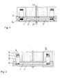
- Fig. 1 shows a contact arrangement of the switching point according to the invention in the closed Status.
- a nominal current IN flows in from a first connection 11 fixed contact 1, a movable, designed as a contact ring 3 Bridge contact and a fixed contact 2 to a second Connection 21.
- the fixed contact 1 is designed as a disc and from surround the fixed contact piece 2, which is substantially cylindrical is trained.
- the two fixed contact pieces 1, which are coaxially interlocked and 2 and the contact ring 3 fitted between them together form the Contact arrangement.
- the contact arrangement is made of an electrically insulating Contact carrier 7 worn. As can be seen from Fig. 2, the circular ring 3 in move in the axial direction.
- the contact arrangement can be opened and the Rated current IN can be interrupted.
- To drive the contact ring 3 contains the Switching point an electrodynamic drive, with two ring-shaped, flat coils 5 and 6.
- the two coils 5 and 6 delimit one in the axial direction Annulus 8, in which the circular ring 3 moves back and forth.
- the annular space 8 is delimited by an insulating body 4 which also has the coil 6 wearing.
- the exact geometric design of the contact arrangement can be seen in FIG. 3.
- the two fixed contact pieces 1 and 2 form a gap 81.
- This gap is so wide that in the closed state of the switching point the contact ring 3 fits exactly and has good electrical contact on both sides with the fixed contact pieces 1 and 2.
- the contact pieces 1 and 2 are provided with contact fingers K against the gap 81.
- the contact fingers K are separated from one another by slots L and have a low spring action in the radial direction. As a result, the mechanical hold of the contact ring 3 in the gap 81 and the electrical contact are improved.
- the first coil 5, which is required for opening the contact arrangement, is attached below the gap 81.
- the contact ring 3 is located at the other end of the annular space 8, in a holding device 10, the task of which is to hold the contact ring 3.
- the second coil 6, which is required for closing the contact arrangement, is attached above the holding device 10.
- the insulating body 4 is pressure-resistant and is gas-tightly attached to the fixed contact pieces 1 and 2.
- the annular space 8 has a region 82 which is widened in the radial direction between the gap 81 and the holding device 10.
- the annular space 8 is filled with a gaseous medium, for example air or SF 6 under atmospheric or higher pressure.
- the two coils 5 and 6 are fed by a power electronic control unit 9.
- 3 and 4 show a first embodiment of the control unit 9 of the switching point according to the invention.
- a first capacitor C S and two thyristors T S1 and T S2 with antiparallel connected freewheeling diodes D S2 and D S1 are connected to coil 6 to form a first circuit.
- a second capacitor C O and two further thyristors T O1 and T O2 with antiparallel switched freewheeling diodes D O2 and D O1 with the coil 5 are connected to a second resonant circuit.
- the functioning of the drive of the switching point is explained on the basis of a closing process, as is shown in FIG. 3.
- the contact ring 3 is located in the holding device 10, the capacitor C S is positively charged and the two thyristors T S1 and T S2 are blocked.
- the capacitor C S is discharged via T S1 , the coil 6 and the freewheeling diode D S1 .
- the result is a sinusoidal current pulse I S in the drive coil 6, which causes an eddy current I W in the contact ring 3 directly below it.
- the drive current Is and the eddy current I W have opposite directions, which results in a repulsive effect Fs between the contact ring 3 and coil 6.
- the coil 6 is firmly connected to the insulating body 4.
- the contact ring 3 is accelerated downwards and is only dampened when it enters the gap 81 by an air cushion enclosed in the gap 81 and by friction. When it hits the coil 5 underneath it, it is finally braked.
- the capacitor C S forms a series resonant circuit with the coil 6. A one-time firing of the thyristor T S1 thus results in the capacitor C S swinging over.
- the capacitor C S is now negatively charged with a voltage slightly lower than the original voltage, since the ohmic resistors in the circuit result in electrical losses.
- the thyristor T S2 is ignited, with which the capacitor C S is recharged a second time via T S2 , the coil 6 and the free-wheeling diode D S2 . Due to the greater distance between the contact ring 3 and the coil 6, there is now a smaller force pulse F S on the contact ring. However, this is sufficient to prevent the ring from rebounding from the fully closed position.
- the successive firing of the thyristors T S1 and T S2 has the essential advantage that the fixed contact pieces 1 and 2 do not have to be dimensioned according to the braking force on the contact ring 3 during the closing process.
- the contact ring 3 only has to have sufficient kinetic energy to reach the completely closed position against the friction of the fixed contact pieces 1 and 2. Bouncing back from there is not possible due to the second power surge that follows.
- the second triggering also has the advantage that the capacitor C S swings around again and is therefore positively charged again.
- a charging device that can only generate positive charging voltages can now be switched on again directly in order to recharge the capacitor C S. Because of the residual charge voltage already present, this recharging process will also be significantly faster than a recharging process. For applications in which repeated triggering is required, the charging device can thus be made smaller.
- An opening process corresponds essentially to the closing process.
- the contact ring 3 is located in the gap 81, the capacitor C O is positively charged and the two thyristors T O1 and T O2 are blocked.
- the capacitor C O is discharged via T O1 (T O2 ), the coil 5 and the freewheeling diode D O1 (D O2 ).
- the current in turn causes an eddy current in the contact ring 3, which is then accelerated in the axial direction and detached from the fixed contact pieces 1 and 2 to form two partial arcs connected in series.
- the contact ring 3 moves in the annular space 8 in the axial direction and is only delayed again by the holding device 10.
- the holding device 10 is designed in the form of a narrowing of the annular space 8.
- the contact ring is completely braked and held in place by friction.
- the slots L in the fixed contact pieces 1 and 2 prevent eddy current formation in the fixed contact pieces 1 and 2.
- the slots L run away from the gap 81 in the radial direction and have a length of about 1 cm.
- the drive is based on both the closing process and the opening process the principle of electrodynamic repulsion. It is particularly advantageous that only the contact ring 3 is moved mechanically. No further is needed moving parts for power transmission, triggering or energy storage.
- the Electrodynamic drive also has the advantages of exact triggerability Ignition of a thyristor, the short-term, fast-acting and very high Impulse force and the uniform force effect on the contact ring. Thanks to the axially symmetrical design of the contact arrangement of the switching point according to the Invention is the contact ring 3 without mechanical guide elements by the expanded area 82 of the annular space 8 out.
- the holding device with the conical extending constriction 10 at the upper end of the annulus 8 and conical bevelled, fixed contact pieces 1 and 2 at the lower end of the Annulus 8 inherently center the contact ring 3.
- the inner geometry of the annular space 8 can be used to advantage Contact ring 3 to delay during the opening process or in order Annulus 8 a suitable flow of the gaseous medium present there to reach. This is vital when the contact ring 3 becomes one Loses contact time at which the nominal current IN is not zero. Also at The existence of a low-impedance and low-inductance parallel path will increase Commutation arcs between the fixed contact pieces 1 and 2 and form the contact ring 3, which by the flow in the annular space 8 and through the insulating body 4 are cooled. This has a higher arc voltage Consequence, which in turn accelerates the commutation process.
- the geometric mass of the contact arrangement of the switching point according to the invention depend on the nominal electrical data of the switching point. At a nominal current IN the switching point of 5 kA and a nominal voltage of 12 kV is the Diameter of the contact ring 3 approx. 250 mm. Its the width of the gap 81 corresponding thickness is 8 mm. At a height of a few millimeters, it's over silver-plated aluminum built contact ring 3 a mass of some 10 to 100 gram. The switching time for a switching point of this size is approx. 1 ms per Switching operation.
Landscapes
- Driving Mechanisms And Operating Circuits Of Arc-Extinguishing High-Tension Switches (AREA)
- Relay Circuits (AREA)
- Linear Motors (AREA)
Priority Applications (5)
| Application Number | Priority Date | Filing Date | Title |
|---|---|---|---|
| EP99810596A EP1067569B1 (fr) | 1999-07-06 | 1999-07-06 | Dispositif mécanique de commutation rapide |
| DE59913821T DE59913821D1 (de) | 1999-07-06 | 1999-07-06 | Schnelle mechanische Schaltstelle |
| JP2000202526A JP2001057142A (ja) | 1999-07-06 | 2000-07-04 | 速く切換わる機械的な切換接点 |
| US09/610,619 US6501635B1 (en) | 1999-07-06 | 2000-07-05 | Quick-action mechanical switching point |
| CNB00119996XA CN1169172C (zh) | 1999-07-06 | 2000-07-06 | 快速反应的机械开关点 |
Applications Claiming Priority (1)
| Application Number | Priority Date | Filing Date | Title |
|---|---|---|---|
| EP99810596A EP1067569B1 (fr) | 1999-07-06 | 1999-07-06 | Dispositif mécanique de commutation rapide |
Publications (2)
| Publication Number | Publication Date |
|---|---|
| EP1067569A1 true EP1067569A1 (fr) | 2001-01-10 |
| EP1067569B1 EP1067569B1 (fr) | 2006-08-30 |
Family
ID=8242910
Family Applications (1)
| Application Number | Title | Priority Date | Filing Date |
|---|---|---|---|
| EP99810596A Expired - Lifetime EP1067569B1 (fr) | 1999-07-06 | 1999-07-06 | Dispositif mécanique de commutation rapide |
Country Status (5)
| Country | Link |
|---|---|
| US (1) | US6501635B1 (fr) |
| EP (1) | EP1067569B1 (fr) |
| JP (1) | JP2001057142A (fr) |
| CN (1) | CN1169172C (fr) |
| DE (1) | DE59913821D1 (fr) |
Cited By (2)
| Publication number | Priority date | Publication date | Assignee | Title |
|---|---|---|---|---|
| US6808854B2 (en) | 2001-04-27 | 2004-10-26 | Canon Kabushiki Kaisha | Polyhydroxyalkanoates having in its side chain phenylsulfinyl structure and/or phenyl sulfonyl structure and production process therefor; charge control agent, toner binder and toner containing same; and image forming method and image forming apparatus using the toner |
| EP2339599A1 (fr) * | 2009-12-22 | 2011-06-29 | ABB Research Ltd. | Commutateur et utilisation associée |
Families Citing this family (4)
| Publication number | Priority date | Publication date | Assignee | Title |
|---|---|---|---|---|
| CN105206449B (zh) * | 2009-11-16 | 2018-01-02 | Abb 技术有限公司 | 使输电线路或配电线路的电流断路的装置和方法以及限流布置 |
| US8890019B2 (en) | 2011-02-05 | 2014-11-18 | Roger Webster Faulkner | Commutating circuit breaker |
| US11646575B2 (en) | 2018-10-24 | 2023-05-09 | The Florida State University Research Foundation, Inc. | Direct current hybrid circuit breaker with reverse biased voltage source |
| US11424093B2 (en) | 2018-10-24 | 2022-08-23 | The Florida State University Research Foundation, Inc. | Direct current hybrid circuit breaker with reverse biased voltage source |
Citations (6)
| Publication number | Priority date | Publication date | Assignee | Title |
|---|---|---|---|---|
| US2951188A (en) * | 1956-01-10 | 1960-08-30 | Ite Circuit Breaker Ltd | High speed contacting device |
| CH348442A (de) * | 1955-12-28 | 1960-08-31 | Siemens Ag | Elektrodynamische Antriebsanordnung für hin und her gehende Bewegung |
| DE1091658B (de) * | 1955-12-29 | 1960-10-27 | Siemens Ag | Anordnung zur Ausloesung und Betaetigung einer Hochspannungsschalteinrichtung mit auf Hochspannungspotential befindlichem elektromechanischem Antrieb |
| US3268687A (en) * | 1963-05-20 | 1966-08-23 | Waghorne John Henry | High speed device for interrupting and completing high voltage power circuits |
| EP0147036A1 (fr) * | 1983-11-25 | 1985-07-03 | The Electricity Council | Arrangement pour disjoncteur |
| EP0800195A2 (fr) * | 1996-04-03 | 1997-10-08 | Mitsubishi Denki Kabushiki Kaisha | Appareilage de commutation |
-
1999
- 1999-07-06 DE DE59913821T patent/DE59913821D1/de not_active Expired - Lifetime
- 1999-07-06 EP EP99810596A patent/EP1067569B1/fr not_active Expired - Lifetime
-
2000
- 2000-07-04 JP JP2000202526A patent/JP2001057142A/ja not_active Withdrawn
- 2000-07-05 US US09/610,619 patent/US6501635B1/en not_active Expired - Fee Related
- 2000-07-06 CN CNB00119996XA patent/CN1169172C/zh not_active Expired - Fee Related
Patent Citations (6)
| Publication number | Priority date | Publication date | Assignee | Title |
|---|---|---|---|---|
| CH348442A (de) * | 1955-12-28 | 1960-08-31 | Siemens Ag | Elektrodynamische Antriebsanordnung für hin und her gehende Bewegung |
| DE1091658B (de) * | 1955-12-29 | 1960-10-27 | Siemens Ag | Anordnung zur Ausloesung und Betaetigung einer Hochspannungsschalteinrichtung mit auf Hochspannungspotential befindlichem elektromechanischem Antrieb |
| US2951188A (en) * | 1956-01-10 | 1960-08-30 | Ite Circuit Breaker Ltd | High speed contacting device |
| US3268687A (en) * | 1963-05-20 | 1966-08-23 | Waghorne John Henry | High speed device for interrupting and completing high voltage power circuits |
| EP0147036A1 (fr) * | 1983-11-25 | 1985-07-03 | The Electricity Council | Arrangement pour disjoncteur |
| EP0800195A2 (fr) * | 1996-04-03 | 1997-10-08 | Mitsubishi Denki Kabushiki Kaisha | Appareilage de commutation |
Cited By (2)
| Publication number | Priority date | Publication date | Assignee | Title |
|---|---|---|---|---|
| US6808854B2 (en) | 2001-04-27 | 2004-10-26 | Canon Kabushiki Kaisha | Polyhydroxyalkanoates having in its side chain phenylsulfinyl structure and/or phenyl sulfonyl structure and production process therefor; charge control agent, toner binder and toner containing same; and image forming method and image forming apparatus using the toner |
| EP2339599A1 (fr) * | 2009-12-22 | 2011-06-29 | ABB Research Ltd. | Commutateur et utilisation associée |
Also Published As
| Publication number | Publication date |
|---|---|
| US6501635B1 (en) | 2002-12-31 |
| EP1067569B1 (fr) | 2006-08-30 |
| DE59913821D1 (de) | 2006-10-12 |
| CN1292562A (zh) | 2001-04-25 |
| JP2001057142A (ja) | 2001-02-27 |
| CN1169172C (zh) | 2004-09-29 |
Similar Documents
| Publication | Publication Date | Title |
|---|---|---|
| EP0844631B1 (fr) | Appareillage de commutation électrique | |
| DE69013300T2 (de) | Überspannungsbegrenzender Schalter. | |
| DE2600683C2 (de) | Strombegrenzungsanordnung mit einem Vakuumschalter | |
| US20220029408A1 (en) | Current cut-off device for high-voltage direct current with capacitive buffer circuit, and control method | |
| EP1014403A1 (fr) | Interrupteur limiteur de courant | |
| EP1766646B1 (fr) | Ampoule sous vide et ensemble de contacts pour un disjoncteur a vide | |
| DE19953551C1 (de) | Schneller strombegrenzender Schalter | |
| EP1067569B1 (fr) | Dispositif mécanique de commutation rapide | |
| EP1675142A1 (fr) | Système de contact pour un appareil de commutation électrique | |
| DE102016115222A1 (de) | Kurzschließeinrichtung für den Einsatz in Nieder- und Mittelspannungsanlagen zum Sach- und Personenschutz | |
| EP2309526B1 (fr) | Commutateur de puissance avec des branches de courant nominal parallèles | |
| EP2728602A1 (fr) | Séparateur de charge haute tension électrique et procédé d'ouverture de celui-ci | |
| EP3039703B1 (fr) | Disjoncteur haute tension à isolation gazeuse | |
| DE10002870A1 (de) | Vorrichtung zum Begrenzen eines Stromes | |
| EP3561846B1 (fr) | Disjoncteur à vide | |
| DE4027723A1 (de) | Vakuumschaltkammer fuer lasttrennschalter | |
| EP3050069B1 (fr) | Un dispositif de commutation et procédé de coupure de fonctionnement d'un dispositif de commutation | |
| EP0104599B1 (fr) | Sectionneur haute tension avec contacts préliminaires | |
| DE2014101A1 (de) | Elektrischer Schalter | |
| EP3561845A1 (fr) | Tube commutateur à vide | |
| DE3224778A1 (de) | Hochspannungsschaltkammer mit hilfslichtbogen | |
| EP3561972A1 (fr) | Installation d'influence de réseau | |
| EP1022755B1 (fr) | Interrupteur limiteur de courant | |
| EP0776021A2 (fr) | Dispositif de commutation électrique | |
| WO2026073737A1 (fr) | Commutateur hybride et procédé de commande d'un commutateur hybride |
Legal Events
| Date | Code | Title | Description |
|---|---|---|---|
| PUAI | Public reference made under article 153(3) epc to a published international application that has entered the european phase |
Free format text: ORIGINAL CODE: 0009012 |
|
| AK | Designated contracting states |
Kind code of ref document: A1 Designated state(s): CH DE FR GB IT LI SE |
|
| AX | Request for extension of the european patent |
Free format text: AL;LT;LV;MK;RO;SI |
|
| 17P | Request for examination filed |
Effective date: 20010519 |
|
| AKX | Designation fees paid |
Free format text: CH DE FR GB IT LI SE |
|
| RAP1 | Party data changed (applicant data changed or rights of an application transferred) |
Owner name: ABB SCHWEIZ AG |
|
| GRAP | Despatch of communication of intention to grant a patent |
Free format text: ORIGINAL CODE: EPIDOSNIGR1 |
|
| GRAS | Grant fee paid |
Free format text: ORIGINAL CODE: EPIDOSNIGR3 |
|
| GRAA | (expected) grant |
Free format text: ORIGINAL CODE: 0009210 |
|
| AK | Designated contracting states |
Kind code of ref document: B1 Designated state(s): CH DE FR GB IT LI SE |
|
| PG25 | Lapsed in a contracting state [announced via postgrant information from national office to epo] |
Ref country code: IT Free format text: LAPSE BECAUSE OF FAILURE TO SUBMIT A TRANSLATION OF THE DESCRIPTION OR TO PAY THE FEE WITHIN THE PRESCRIBED TIME-LIMIT;WARNING: LAPSES OF ITALIAN PATENTS WITH EFFECTIVE DATE BEFORE 2007 MAY HAVE OCCURRED AT ANY TIME BEFORE 2007. THE CORRECT EFFECTIVE DATE MAY BE DIFFERENT FROM THE ONE RECORDED. Effective date: 20060830 |
|
| REG | Reference to a national code |
Ref country code: GB Ref legal event code: FG4D Free format text: NOT ENGLISH |
|
| REG | Reference to a national code |
Ref country code: CH Ref legal event code: EP |
|
| REF | Corresponds to: |
Ref document number: 59913821 Country of ref document: DE Date of ref document: 20061012 Kind code of ref document: P |
|
| PG25 | Lapsed in a contracting state [announced via postgrant information from national office to epo] |
Ref country code: SE Free format text: LAPSE BECAUSE OF FAILURE TO SUBMIT A TRANSLATION OF THE DESCRIPTION OR TO PAY THE FEE WITHIN THE PRESCRIBED TIME-LIMIT Effective date: 20061130 |
|
| GBT | Gb: translation of ep patent filed (gb section 77(6)(a)/1977) |
Effective date: 20061122 |
|
| ET | Fr: translation filed | ||
| PLBE | No opposition filed within time limit |
Free format text: ORIGINAL CODE: 0009261 |
|
| STAA | Information on the status of an ep patent application or granted ep patent |
Free format text: STATUS: NO OPPOSITION FILED WITHIN TIME LIMIT |
|
| 26N | No opposition filed |
Effective date: 20070531 |
|
| REG | Reference to a national code |
Ref country code: CH Ref legal event code: PL |
|
| PG25 | Lapsed in a contracting state [announced via postgrant information from national office to epo] |
Ref country code: LI Free format text: LAPSE BECAUSE OF NON-PAYMENT OF DUE FEES Effective date: 20070731 Ref country code: CH Free format text: LAPSE BECAUSE OF NON-PAYMENT OF DUE FEES Effective date: 20070731 |
|
| PGFP | Annual fee paid to national office [announced via postgrant information from national office to epo] |
Ref country code: GB Payment date: 20120719 Year of fee payment: 14 |
|
| PGFP | Annual fee paid to national office [announced via postgrant information from national office to epo] |
Ref country code: FR Payment date: 20120806 Year of fee payment: 14 Ref country code: IT Payment date: 20120726 Year of fee payment: 14 Ref country code: DE Payment date: 20120720 Year of fee payment: 14 |
|
| GBPC | Gb: european patent ceased through non-payment of renewal fee |
Effective date: 20130706 |
|
| REG | Reference to a national code |
Ref country code: DE Ref legal event code: R119 Ref document number: 59913821 Country of ref document: DE Effective date: 20140201 |
|
| REG | Reference to a national code |
Ref country code: FR Ref legal event code: ST Effective date: 20140331 |
|
| PG25 | Lapsed in a contracting state [announced via postgrant information from national office to epo] |
Ref country code: GB Free format text: LAPSE BECAUSE OF NON-PAYMENT OF DUE FEES Effective date: 20130706 Ref country code: DE Free format text: LAPSE BECAUSE OF NON-PAYMENT OF DUE FEES Effective date: 20140201 |
|
| PG25 | Lapsed in a contracting state [announced via postgrant information from national office to epo] |
Ref country code: FR Free format text: LAPSE BECAUSE OF NON-PAYMENT OF DUE FEES Effective date: 20130731 Ref country code: IT Free format text: LAPSE BECAUSE OF NON-PAYMENT OF DUE FEES Effective date: 20130706 |