EP1067599A1 - Méthode de formation de structures comportant des régions oxidées enfouies dans un substrat semiconducteur - Google Patents
Méthode de formation de structures comportant des régions oxidées enfouies dans un substrat semiconducteur Download PDFInfo
- Publication number
- EP1067599A1 EP1067599A1 EP99830442A EP99830442A EP1067599A1 EP 1067599 A1 EP1067599 A1 EP 1067599A1 EP 99830442 A EP99830442 A EP 99830442A EP 99830442 A EP99830442 A EP 99830442A EP 1067599 A1 EP1067599 A1 EP 1067599A1
- Authority
- EP
- European Patent Office
- Prior art keywords
- substrate
- region
- silicon
- trenches
- conductivity
- Prior art date
- Legal status (The legal status is an assumption and is not a legal conclusion. Google has not performed a legal analysis and makes no representation as to the accuracy of the status listed.)
- Granted
Links
Images


Classifications
-
- H—ELECTRICITY
- H10—SEMICONDUCTOR DEVICES; ELECTRIC SOLID-STATE DEVICES NOT OTHERWISE PROVIDED FOR
- H10W—GENERIC PACKAGES, INTERCONNECTIONS, CONNECTORS OR OTHER CONSTRUCTIONAL DETAILS OF DEVICES COVERED BY CLASS H10
- H10W10/00—Isolation regions in semiconductor bodies between components of integrated devices
- H10W10/01—Manufacture or treatment
- H10W10/011—Manufacture or treatment of isolation regions comprising dielectric materials
- H10W10/012—Manufacture or treatment of isolation regions comprising dielectric materials using local oxidation of silicon [LOCOS]
- H10W10/0121—Manufacture or treatment of isolation regions comprising dielectric materials using local oxidation of silicon [LOCOS] in regions recessed from the surface, e.g. in trenches or grooves
- H10W10/0123—Manufacture or treatment of isolation regions comprising dielectric materials using local oxidation of silicon [LOCOS] in regions recessed from the surface, e.g. in trenches or grooves using auxiliary pillars in the regions
-
- H—ELECTRICITY
- H10—SEMICONDUCTOR DEVICES; ELECTRIC SOLID-STATE DEVICES NOT OTHERWISE PROVIDED FOR
- H10W—GENERIC PACKAGES, INTERCONNECTIONS, CONNECTORS OR OTHER CONSTRUCTIONAL DETAILS OF DEVICES COVERED BY CLASS H10
- H10W10/00—Isolation regions in semiconductor bodies between components of integrated devices
- H10W10/01—Manufacture or treatment
- H10W10/041—Manufacture or treatment of isolation regions comprising polycrystalline semiconductor materials
-
- H—ELECTRICITY
- H10—SEMICONDUCTOR DEVICES; ELECTRIC SOLID-STATE DEVICES NOT OTHERWISE PROVIDED FOR
- H10W—GENERIC PACKAGES, INTERCONNECTIONS, CONNECTORS OR OTHER CONSTRUCTIONAL DETAILS OF DEVICES COVERED BY CLASS H10
- H10W10/00—Isolation regions in semiconductor bodies between components of integrated devices
- H10W10/10—Isolation regions comprising dielectric materials
- H10W10/13—Isolation regions comprising dielectric materials formed using local oxidation of silicon [LOCOS], e.g. sealed interface localised oxidation [SILO] or side-wall mask isolation [SWAMI]
-
- H—ELECTRICITY
- H10—SEMICONDUCTOR DEVICES; ELECTRIC SOLID-STATE DEVICES NOT OTHERWISE PROVIDED FOR
- H10W—GENERIC PACKAGES, INTERCONNECTIONS, CONNECTORS OR OTHER CONSTRUCTIONAL DETAILS OF DEVICES COVERED BY CLASS H10
- H10W10/00—Isolation regions in semiconductor bodies between components of integrated devices
- H10W10/40—Isolation regions comprising polycrystalline semiconductor materials
Definitions
- a particular object of the present invention is to propose a method which enables high-performance devices with dielectric insulation and buried regions to be formed.
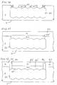
- the polycrystalline silicon layer 52 is partially removed by dry etching and is then oxidized so as to form a silicon dioxide insert 53 in the mouth of the channel 50 until the channel is closed ( Figure 14).
Landscapes
- Element Separation (AREA)
Priority Applications (4)
| Application Number | Priority Date | Filing Date | Title |
|---|---|---|---|
| DE69937106T DE69937106T2 (de) | 1999-07-09 | 1999-07-09 | Verfahren zur Herstellung von Strukturen mit vergrabenen Oxidbereichen in einem Halbleitersubstrat |
| EP99830442A EP1067599B1 (fr) | 1999-07-09 | 1999-07-09 | Méthode de formation de structures comportant des régions oxidées enfouies dans un substrat semiconducteur |
| JP2000208131A JP2001044399A (ja) | 1999-07-09 | 2000-07-10 | 半導体装置の製造方法 |
| US09/613,109 US6455391B1 (en) | 1999-07-09 | 2000-07-10 | Method of forming structures with buried regions in a semiconductor device |
Applications Claiming Priority (1)
| Application Number | Priority Date | Filing Date | Title |
|---|---|---|---|
| EP99830442A EP1067599B1 (fr) | 1999-07-09 | 1999-07-09 | Méthode de formation de structures comportant des régions oxidées enfouies dans un substrat semiconducteur |
Publications (2)
| Publication Number | Publication Date |
|---|---|
| EP1067599A1 true EP1067599A1 (fr) | 2001-01-10 |
| EP1067599B1 EP1067599B1 (fr) | 2007-09-12 |
Family
ID=8243498
Family Applications (1)
| Application Number | Title | Priority Date | Filing Date |
|---|---|---|---|
| EP99830442A Expired - Lifetime EP1067599B1 (fr) | 1999-07-09 | 1999-07-09 | Méthode de formation de structures comportant des régions oxidées enfouies dans un substrat semiconducteur |
Country Status (4)
| Country | Link |
|---|---|
| US (1) | US6455391B1 (fr) |
| EP (1) | EP1067599B1 (fr) |
| JP (1) | JP2001044399A (fr) |
| DE (1) | DE69937106T2 (fr) |
Cited By (4)
| Publication number | Priority date | Publication date | Assignee | Title |
|---|---|---|---|---|
| US6455391B1 (en) | 1999-07-09 | 2002-09-24 | Stmicroelectronics S.R.L. | Method of forming structures with buried regions in a semiconductor device |
| EP1427011A1 (fr) * | 2002-12-04 | 2004-06-09 | STMicroelectronics S.r.l. | Procédé de réalisation de micro-canaux dans une structure intégrée |
| US7294536B2 (en) | 2000-07-25 | 2007-11-13 | Stmicroelectronics S.R.L. | Process for manufacturing an SOI wafer by annealing and oxidation of buried channels |
| CN105074922A (zh) * | 2013-06-14 | 2015-11-18 | 富士电机株式会社 | 半导体器件 |
Families Citing this family (3)
| Publication number | Priority date | Publication date | Assignee | Title |
|---|---|---|---|---|
| JP2000058802A (ja) * | 1998-01-13 | 2000-02-25 | Stmicroelectronics Srl | Soiウェハの製造方法 |
| JP5757145B2 (ja) * | 2011-04-19 | 2015-07-29 | 富士電機株式会社 | 半導体装置 |
| CN110858561A (zh) * | 2018-08-23 | 2020-03-03 | 合肥晶合集成电路有限公司 | 硅岛结构及其制作方法 |
Citations (6)
| Publication number | Priority date | Publication date | Assignee | Title |
|---|---|---|---|---|
| JPS5612749A (en) * | 1979-07-12 | 1981-02-07 | Matsushita Electric Ind Co Ltd | Production of semiconductor device |
| US4502913A (en) * | 1982-06-30 | 1985-03-05 | International Business Machines Corporation | Total dielectric isolation for integrated circuits |
| US4604162A (en) * | 1983-06-13 | 1986-08-05 | Ncr Corporation | Formation and planarization of silicon-on-insulator structures |
| US4814287A (en) * | 1983-09-28 | 1989-03-21 | Matsushita Electric Industrial Co. Ltd. | Method of manufacturing a semiconductor integrated circuit device |
| US4891092A (en) * | 1986-01-13 | 1990-01-02 | General Electric Company | Method for making a silicon-on-insulator substrate |
| EP0929095A1 (fr) * | 1998-01-13 | 1999-07-14 | STMicroelectronics S.r.l. | Procédé pour fabriquer un substrat du type SOI |
Family Cites Families (2)
| Publication number | Priority date | Publication date | Assignee | Title |
|---|---|---|---|---|
| US5907782A (en) * | 1998-08-15 | 1999-05-25 | Acer Semiconductor Manufacturing Inc. | Method of forming a multiple fin-pillar capacitor for a high density dram cell |
| DE69937106T2 (de) | 1999-07-09 | 2008-06-05 | Stmicroelectronics S.R.L., Agrate Brianza | Verfahren zur Herstellung von Strukturen mit vergrabenen Oxidbereichen in einem Halbleitersubstrat |
-
1999
- 1999-07-09 DE DE69937106T patent/DE69937106T2/de not_active Expired - Lifetime
- 1999-07-09 EP EP99830442A patent/EP1067599B1/fr not_active Expired - Lifetime
-
2000
- 2000-07-10 JP JP2000208131A patent/JP2001044399A/ja active Pending
- 2000-07-10 US US09/613,109 patent/US6455391B1/en not_active Expired - Lifetime
Patent Citations (6)
| Publication number | Priority date | Publication date | Assignee | Title |
|---|---|---|---|---|
| JPS5612749A (en) * | 1979-07-12 | 1981-02-07 | Matsushita Electric Ind Co Ltd | Production of semiconductor device |
| US4502913A (en) * | 1982-06-30 | 1985-03-05 | International Business Machines Corporation | Total dielectric isolation for integrated circuits |
| US4604162A (en) * | 1983-06-13 | 1986-08-05 | Ncr Corporation | Formation and planarization of silicon-on-insulator structures |
| US4814287A (en) * | 1983-09-28 | 1989-03-21 | Matsushita Electric Industrial Co. Ltd. | Method of manufacturing a semiconductor integrated circuit device |
| US4891092A (en) * | 1986-01-13 | 1990-01-02 | General Electric Company | Method for making a silicon-on-insulator substrate |
| EP0929095A1 (fr) * | 1998-01-13 | 1999-07-14 | STMicroelectronics S.r.l. | Procédé pour fabriquer un substrat du type SOI |
Non-Patent Citations (1)
| Title |
|---|
| PATENT ABSTRACTS OF JAPAN vol. 005, no. 063 (E - 054) 28 April 1981 (1981-04-28) * |
Cited By (10)
| Publication number | Priority date | Publication date | Assignee | Title |
|---|---|---|---|---|
| US6455391B1 (en) | 1999-07-09 | 2002-09-24 | Stmicroelectronics S.R.L. | Method of forming structures with buried regions in a semiconductor device |
| US7294536B2 (en) | 2000-07-25 | 2007-11-13 | Stmicroelectronics S.R.L. | Process for manufacturing an SOI wafer by annealing and oxidation of buried channels |
| US7754578B2 (en) | 2001-12-28 | 2010-07-13 | Stmicroelectronics, S.R.L. | Process for manufacturing a wafer by annealing of buried channels |
| US8334188B2 (en) | 2001-12-28 | 2012-12-18 | Stmicroelectronics S.R.L. | Process for manufacturing a wafer by annealing of buried channels |
| EP1427011A1 (fr) * | 2002-12-04 | 2004-06-09 | STMicroelectronics S.r.l. | Procédé de réalisation de micro-canaux dans une structure intégrée |
| US7063798B2 (en) | 2002-12-04 | 2006-06-20 | Stmicroelectronics S.R.L. | Method for realizing microchannels in an integrated structure |
| CN105074922A (zh) * | 2013-06-14 | 2015-11-18 | 富士电机株式会社 | 半导体器件 |
| EP3010042A4 (fr) * | 2013-06-14 | 2017-01-18 | Fuji Electric Co., Ltd. | Dispositif à semi-conducteurs |
| US10002961B2 (en) | 2013-06-14 | 2018-06-19 | Fuji Electric Co., Ltd. | Semiconductor device suppressing current leakage in a bootstrap diode |
| CN105074922B (zh) * | 2013-06-14 | 2018-07-03 | 富士电机株式会社 | 半导体器件 |
Also Published As
| Publication number | Publication date |
|---|---|
| JP2001044399A (ja) | 2001-02-16 |
| DE69937106D1 (de) | 2007-10-25 |
| US6455391B1 (en) | 2002-09-24 |
| EP1067599B1 (fr) | 2007-09-12 |
| DE69937106T2 (de) | 2008-06-05 |
Similar Documents
| Publication | Publication Date | Title |
|---|---|---|
| EP1043775B1 (fr) | Circuit intégré de puissance ayant un courant vertical et son procédé de fabrication | |
| US6168996B1 (en) | Method of fabricating semiconductor device | |
| JPH05102296A (ja) | 集積回路において平坦化した浅いトレンチ分離を製造する方法及びそれにより製造された構成体 | |
| KR20010021740A (ko) | 무선 주파수에서 사용되는 집적 회로 소자를 제조하는 방법 | |
| US5049521A (en) | Method for forming dielectrically isolated semiconductor devices with contact to the wafer substrate | |
| US5856700A (en) | Semiconductor device with doped semiconductor and dielectric trench sidewall layers | |
| US4992843A (en) | Collector contact of an integrated bipolar transistor | |
| US6599810B1 (en) | Shallow trench isolation formation with ion implantation | |
| US6331470B1 (en) | Process for manufacturing a semiconductor material wafer having power regions dielectrically insulated from circuitry regions | |
| EP1067599B1 (fr) | Méthode de formation de structures comportant des régions oxidées enfouies dans un substrat semiconducteur | |
| US6617646B2 (en) | Reduced substrate capacitance high performance SOI process | |
| KR100854077B1 (ko) | 웨이퍼 본딩을 이용한 soi 기판 제조 방법과 이 soi기판을 사용한 상보형 고전압 바이폴라 트랜지스터 제조방법 | |
| JP2000349289A (ja) | 半導体装置およびその製造方法 | |
| KR19990071491A (ko) | 적어도 하나 이상의 mos 트랜지스터를 가진 집적 회로장치를 제조하기 위한 방법 | |
| US6727569B1 (en) | Method of making enhanced trench oxide with low temperature nitrogen integration | |
| JP2850527B2 (ja) | 半導体装置およびその製造方法 | |
| JP3142336B2 (ja) | 半導体装置及びその製造方法 | |
| EP0253538A2 (fr) | Transistor bipolaire VLSI autoaligné | |
| US20030006487A1 (en) | Semiconductor device having element isolation structure | |
| JP3257523B2 (ja) | 半導体装置の製造方法 | |
| KR100249022B1 (ko) | 반도체장치의 소자 격리 방법 | |
| JPS5992546A (ja) | バイポ−ラ集積回路装置 | |
| JP2000031489A (ja) | 半導体装置の製造方法 | |
| JPH05109884A (ja) | 半導体装置の製造方法 | |
| JP2000260780A (ja) | 半導体装置およびその製造方法 |
Legal Events
| Date | Code | Title | Description |
|---|---|---|---|
| PUAI | Public reference made under article 153(3) epc to a published international application that has entered the european phase |
Free format text: ORIGINAL CODE: 0009012 |
|
| AK | Designated contracting states |
Kind code of ref document: A1 Designated state(s): DE FR GB IT |
|
| AX | Request for extension of the european patent |
Free format text: AL;LT;LV;MK;RO;SI |
|
| 17P | Request for examination filed |
Effective date: 20010615 |
|
| AKX | Designation fees paid |
Free format text: DE FR GB IT |
|
| GRAP | Despatch of communication of intention to grant a patent |
Free format text: ORIGINAL CODE: EPIDOSNIGR1 |
|
| GRAS | Grant fee paid |
Free format text: ORIGINAL CODE: EPIDOSNIGR3 |
|
| GRAA | (expected) grant |
Free format text: ORIGINAL CODE: 0009210 |
|
| AK | Designated contracting states |
Kind code of ref document: B1 Designated state(s): DE FR GB IT |
|
| REG | Reference to a national code |
Ref country code: GB Ref legal event code: FG4D |
|
| REF | Corresponds to: |
Ref document number: 69937106 Country of ref document: DE Date of ref document: 20071025 Kind code of ref document: P |
|
| ET | Fr: translation filed | ||
| PLBE | No opposition filed within time limit |
Free format text: ORIGINAL CODE: 0009261 |
|
| STAA | Information on the status of an ep patent application or granted ep patent |
Free format text: STATUS: NO OPPOSITION FILED WITHIN TIME LIMIT |
|
| 26N | No opposition filed |
Effective date: 20080613 |
|
| GBPC | Gb: european patent ceased through non-payment of renewal fee |
Effective date: 20080709 |
|
| PG25 | Lapsed in a contracting state [announced via postgrant information from national office to epo] |
Ref country code: GB Free format text: LAPSE BECAUSE OF NON-PAYMENT OF DUE FEES Effective date: 20080709 |
|
| PG25 | Lapsed in a contracting state [announced via postgrant information from national office to epo] |
Ref country code: IT Free format text: LAPSE BECAUSE OF NON-PAYMENT OF DUE FEES Effective date: 20080709 |
|
| PGFP | Annual fee paid to national office [announced via postgrant information from national office to epo] |
Ref country code: DE Payment date: 20130621 Year of fee payment: 15 |
|
| PGFP | Annual fee paid to national office [announced via postgrant information from national office to epo] |
Ref country code: FR Payment date: 20130722 Year of fee payment: 15 |
|
| REG | Reference to a national code |
Ref country code: DE Ref legal event code: R119 Ref document number: 69937106 Country of ref document: DE |
|
| REG | Reference to a national code |
Ref country code: FR Ref legal event code: ST Effective date: 20150331 |
|
| PG25 | Lapsed in a contracting state [announced via postgrant information from national office to epo] |
Ref country code: DE Free format text: LAPSE BECAUSE OF NON-PAYMENT OF DUE FEES Effective date: 20150203 |
|
| REG | Reference to a national code |
Ref country code: DE Ref legal event code: R119 Ref document number: 69937106 Country of ref document: DE Effective date: 20150203 |
|
| PG25 | Lapsed in a contracting state [announced via postgrant information from national office to epo] |
Ref country code: FR Free format text: LAPSE BECAUSE OF NON-PAYMENT OF DUE FEES Effective date: 20140731 |