EP1067766A2 - Bildaufnahmegerät - Google Patents
Bildaufnahmegerät Download PDFInfo
- Publication number
- EP1067766A2 EP1067766A2 EP00305749A EP00305749A EP1067766A2 EP 1067766 A2 EP1067766 A2 EP 1067766A2 EP 00305749 A EP00305749 A EP 00305749A EP 00305749 A EP00305749 A EP 00305749A EP 1067766 A2 EP1067766 A2 EP 1067766A2
- Authority
- EP
- European Patent Office
- Prior art keywords
- signal
- difference
- image pickup
- photoelectric conversion
- read
- Prior art date
- Legal status (The legal status is an assumption and is not a legal conclusion. Google has not performed a legal analysis and makes no representation as to the accuracy of the status listed.)
- Granted
Links
- 238000001514 detection method Methods 0.000 claims abstract description 55
- 238000006243 chemical reaction Methods 0.000 claims abstract description 45
- 238000012937 correction Methods 0.000 claims abstract description 41
- 238000012545 processing Methods 0.000 claims abstract description 33
- 230000003287 optical effect Effects 0.000 claims abstract description 8
- 230000003321 amplification Effects 0.000 claims description 24
- 238000003199 nucleic acid amplification method Methods 0.000 claims description 24
- 238000012546 transfer Methods 0.000 claims description 16
- 230000001678 irradiating effect Effects 0.000 claims 1
- 238000010586 diagram Methods 0.000 description 16
- 238000000034 method Methods 0.000 description 14
- 230000005540 biological transmission Effects 0.000 description 13
- 239000004065 semiconductor Substances 0.000 description 13
- 239000000758 substrate Substances 0.000 description 8
- 239000011521 glass Substances 0.000 description 5
- 238000003705 background correction Methods 0.000 description 4
- 239000000203 mixture Substances 0.000 description 4
- 239000003086 colorant Substances 0.000 description 3
- 230000004888 barrier function Effects 0.000 description 2
- 238000004891 communication Methods 0.000 description 2
- 230000006835 compression Effects 0.000 description 2
- 238000007906 compression Methods 0.000 description 2
- 230000006870 function Effects 0.000 description 2
- 238000003780 insertion Methods 0.000 description 2
- 230000037431 insertion Effects 0.000 description 2
- 238000012856 packing Methods 0.000 description 2
- XAGFODPZIPBFFR-UHFFFAOYSA-N aluminium Chemical compound [Al] XAGFODPZIPBFFR-UHFFFAOYSA-N 0.000 description 1
- 229910052782 aluminium Inorganic materials 0.000 description 1
- 230000006837 decompression Effects 0.000 description 1
- 230000006866 deterioration Effects 0.000 description 1
- 238000002474 experimental method Methods 0.000 description 1
- 239000000284 extract Substances 0.000 description 1
- 230000007274 generation of a signal involved in cell-cell signaling Effects 0.000 description 1
- 238000003384 imaging method Methods 0.000 description 1
- 210000003127 knee Anatomy 0.000 description 1
- 238000005375 photometry Methods 0.000 description 1
- 230000001012 protector Effects 0.000 description 1
- 239000010453 quartz Substances 0.000 description 1
- 238000000926 separation method Methods 0.000 description 1
- VYPSYNLAJGMNEJ-UHFFFAOYSA-N silicon dioxide Inorganic materials O=[Si]=O VYPSYNLAJGMNEJ-UHFFFAOYSA-N 0.000 description 1
- 230000001360 synchronised effect Effects 0.000 description 1
Images




Classifications
-
- H—ELECTRICITY
- H04—ELECTRIC COMMUNICATION TECHNIQUE
- H04N—PICTORIAL COMMUNICATION, e.g. TELEVISION
- H04N25/00—Circuitry of solid-state image sensors [SSIS]; Control thereof
- H04N25/60—Noise processing, e.g. detecting, correcting, reducing or removing noise
- H04N25/62—Detection or reduction of noise due to excess charges produced by the exposure, e.g. smear, blooming, ghost image, crosstalk or leakage between pixels
- H04N25/627—Detection or reduction of inverted contrast or eclipsing effects
Definitions
- the present invention relates to a solid-state image pickup apparatus with an array of a plurality of pixels each having a photoelectric conversion function, and an image pickup system using the solid-state image pickup apparatus.
- Solid-state image pickup elements are roughly classified into charge transfer type elements such as a CCD, and XY address type elements such as a MOS image pickup device.
- this solid-state image pickup element as a sensor provides not only many merits but also demerits.
- One of the demerits is image deterioration called as "smear" generated when a bright object image is picked up.
- part of object light leaks as photo-leak to a vertical transfer register adjacent to a photodiode, and is observed as a white noise band on the image in the vertical direction of the bright object image.
- This phenomenon occurs with a light quantity corresponding to about 60 dB to about 100 dB of light amount with which the photodiode saturates.
- the pixel is generally made up of a photodiode 1, an amplification MOS transistor 2 for amplifying and outputting a signal from the photodiode, a transfer MOS transistor 3 for transferring the signal from the photodiode 1 to the amplification MOS transistor 2, a reset MOS transistor for supplying a reset potential to the gate region of the amplification MOS transistor, and a selection MOS transistor 5 for selectively outputting a signal from the amplification MOS transistor 2. It has been understood that the smear can be avoided substantially when the gate electrode region of the amplification MOS transistor is reset before the signal from the photodiode 1 is transferred to the amplification MOS transistor 2.
- the transfer time from the photodiode to the amplification MOS transistor is several ⁇ s, while an exposure time is 16 or 17 ms for a movie camera such as a video camera.
- the light quantity difference is about 100 dB, and the gate electrode region of the amplification MOS transistor is shielded from light. In this situation, it has been understood that smear is considered not to occur.
- a conventional solid-state image pickup apparatus having a difference means for subtracting a noise component in order to remove a noise component contained in a signal photoelectrically converted and output by a photoelectric conversion means such as a photodiode.
- FIG. 3 is a timing chart showing the operation timing of the solid-state image pickup apparatus in Fig. 2.
- a pixel 6 has the same structure as that of the pixel shown in Fig. 1.
- a reset signal vn obtained when the input of an amplification MOS transistor is reset, is stored in a memory CN7 during a period tl, and a signal vs generated by photoelectric conversion by a photoelectric conversion means is transferred to the input of the amplification MOS transistor during a period t2.
- a signal VS output from the amplification MOS transistor is stored in a memory CS 8.
- the signal VS stored in the memory CS 8 contains the signal (vs) generated by photoelectric conversion and the reset signal (vn).
- the differential amplifier calculates difference VS - vn, and outputs a signal vs free from any noise component, from which signal vs the reset signal as a noise component is removed.
- VN vn + v1
- Fig. 4 is a conceptual view showing this phenomenon.
- the abscissa represents the incident light quantity on the photoelectric conversion means, and the ordinate represents the level of a signal generated in the photoelectric conversion means.
- an image pickup apparatus comprising a plurality of pixels including photoelectric conversion means for converting an optical signal from an object into an electrical signal and read means for reading out the signal from the photoelectric conversion means, difference means for performing difference processing on a noise component contained in the signal read by the read means, detection means for detecting an image pickup condition, and correction means for performing correction of execution of difference processing in accordance with an output from the detection means.
- an image pickup apparatus comprising a plurality of pixels including photoelectric conversion means for converting an optical signal from an object into an electrical signal and read means for reading out the signal from the photoelectric conversion means, difference means for performing difference processing on a noise component contained in the signal read by the read means, detection means for detecting an image pickup condition, and correction means for controlling the difference means in accordance with an output from the detection means.
- an image pickup apparatus comprising a pixel including photoelectric conversion means for converting an optical signal from an object into an electrical signal and read means for reading out the signal from the photoelectric conversion means, difference means for performing difference operation on a noise component contained in the signal read by the read means, detection means for detecting a signal level of noise generated in the pixel, and correction means for correcting the signal read by the read means in accordance with the detection means.
- Fig. 5 shows a solid-state image pickup apparatus 100 according to the first embodiment.
- each pixel is made up of a photodiode 1 serving as a photoelectric conversion means, an amplification MOS transistor 2 serving as a read means for amplifying and outputting a signal from the photodiode, a transfer MOS transistor 3 serving as a transfer means for transferring the signal from the photodiode 1 to the amplification MOS transistor 2, a reset MOS transistor serving as a reset means for supplying a reset potential to the input of the amplification MOS transistor, and a selection MOS transistor 5 serving as a selection means for selectively outputting a signal from the amplification MOS transistor 2.
- a vertical shift register 11 sequentially outputs signals from pixels on horizontal lines in units of lines.
- An S memory 8 accumulates a signal VS as a sum of a photoelectrically conversion signal generated in the photodiode 1 and output from the amplification MOS transistor 2 in the pixel and a reset signal vn which is a noise component.
- An N memory 7 accumulates a signal VN as a sum of the reset signal vn which is a noise signal, and a photo-leak noise signal v1.
- a horizontal shift register 12 outputs signals accumulated in the S memory 8 and N memory 7 in units of lines.
- An amplifier 13 amplifies the signals VS and VN respectively output from the S memory 8 and N memory 7.
- a differential amplifier 9 serves as a difference means for performing difference operation on the signals VS and VN in order to subtract the noise component from the signal VS output from the amplifier 13.
- a level detection circuit 14 serves as a detection means for detecting image pickup conditions including the object conditions of an object to be picked up.
- a switch 15 serves as a correction means for performing correction of (selectively switching between execution/non-execution of difference operation) execution of difference processing in accordance with an output from the level detection circuit 14. When the switch 15 is opened in accordance with an output from the level detection circuit, the differential amplifier does not receive any signal VN, and receives the signal VS not subjected to difference processing.
- An A/D conversion circuit 16 converts an analog signal output from the differential amplifier into a digital signal.
- a timing generator 17 controls the timings of the image pickup area 10 and A/D conversion circuit 16.
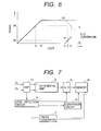
- Fig. 6 is a graph in which the abscissa represents the incident light quantity on the photodiode 1, and the ordinate represents the level of a signal generated in the photodiode.
- the signal vs generated in the photodiode saturates at a light quantity B, and the photo-leak noise v1 gradually reaches a high signal level around a light quantity C.
- the image becomes dark.
- the level detection circuit 14 detects at least whether the signal vs generated in the photodiode saturates or the photo-leak noise signal v1 reaches a predetermined level or more, and when the circuit 14 detects this, the switch 15 is opened to stop difference processing.
- a signal not subjected to difference processing contains a noise component, and is processed as a saturation signal (compressed by Knee processing).
- the signal detected as a saturation signal is set to be a signal at given level VA or more which is slightly smaller than a signal level at which the signal completely saturates.
- the level detection circuit detects whether the signal VS output from the S memory 8 is at signal level VA or more, thereby detecting saturation of the photodiode, or detects whether the signal VN output from the N memory 7 is at signal level VB or more, thereby detecting that the photo-leak noise signal v1 is a predetermined level or more.
- the level detection circuit 14 detects that the signal VS is at signal level VA or more, or the signal VN is at signal level VB or more, difference processing is not executed, thereby obtaining an image free from being darkened.
- the first embodiment has exemplified the level detection circuit 14 as a detection means.
- the detection means suffices to detect image pickup conditions, and may be located not at the output stage of the amplifier 13 but, e.g., within the pixel.
- the first embodiment has exemplified the switch 15 for stopping difference processing as a correction means.
- the correction means suffices to perform correction of execution of difference processing in accordance with an output from the detection means, and may be located in, e.g., the image pickup area 10.
- the correction means may stop transfer of an input or output to or from the N memory 7, or stop transfer of a noise signal from the pixel 6.
- All the building elements of the solid-state image pickup apparatus 100 may be formed on a single semiconductor substrate by the CMOS process or the like.
- the A/D conversion circuit 16 and timing generator may be formed on different semiconductor substrates.
- the pixels of the solid-state image pickup apparatus in the first embodiment may be area sensors arranged two-dimensionally, or line sensors arranged one-dimensionally.
- Fig. 7 is a block diagram showing part of a solid-state image pickup apparatus 100 according to the second embodiment.
- the input stage of an amplifier 13, which is not illustrated in Fig. 7, is the same as that described in the first embodiment.
- a memory 18 accumulates a signal from an A/D conversion circuit 16.
- a conversion circuit 19 serving as a correction means performs correction of execution of difference processing (converts a signal having undergone difference processing into a signal of a predetermined signal level) in accordance with an output of a level detection circuit 14 serving as a detection means.
- the level detection circuit serving as a detection means detects image pickup conditions including the object conditions of an object to be picked up by the same method as in the first embodiment.
- a differential amplifier 9 serving as a difference means executes difference processing (VS-VN) even when a signal VS is detected by the level detection circuit to be at signal level VA or more or even when a signal VN is detected to be at signal level VB or more. Further, the processed signal is converted into a digital signal by the A/D conversion circuit 16, and stored in the memory 18. In reading out a signal from the memory 18, when the signal VS is detected by the level detection circuit to be at signal level VA or more or when the signal VN is detected to be at signal level VB or more, the conversion circuit 19 converts the signal into a signal of a predetermined level (e.g., signal level VA). Alternatively, a digital signal from the A/D conversion circuit 16 may be converted into saturation data upon reception of a saturation detection signal from the level detection circuit 14.
- a predetermined level e.g., signal level VA
- a digital signal from the A/D conversion circuit 16 may be converted into saturation data upon reception of a saturation detection signal from the level detection circuit 14.
- the conversion circuit 19 is operated to obtain an image free from being dardened.
- the second embodiment has exemplified the level detection circuit 14 as a detection means.
- the detection means suffices to detect image pickup conditions, and may be located not at the output stage of the amplifier 13 but, e.g., within the pixel.
- the second embodiment has exemplified as a correction means an arrangement of converting a signal read out from the memory into a signal of a predetermined level.
- the correction means suffices to perform correction of execution of difference processing in accordance with an output of the detection means, and may be located in, e.g., the image pickup area 10.
- All the building elements of the solid-state image pickup apparatus 100 may be formed on a single semiconductor substrate by the CMOS process or the like.
- the A/D conversion circuit 16 and timing generator may be formed on different semiconductor substrates.
- the pixels of the solid-state image pickup apparatus in the second embodiment may be area sensors arranged two-dimensionally, or line sensors arranged one-dimensionally.
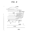
- Fig. 8 is a view showing the section of the pixel.
- the pixel is completely shielded from light in order to prevent any photo-leak.
- a photodiode (corresponding to Fig. 1) is constituted by a region 20 serving as an n-type semiconductor region, and a region 21 serving as a p-type semiconductor region.
- a region 23 serving as an n-type semiconductor region corresponds to the input of the amplification MOS transistor.
- a gate electrode 24 transfers signals from the regions 20 and 21 constituting the photodiode to the region 23.
- Photo-shield films 25, 26, and 27 are made of aluminum, and a black member 28 prevents any photo-leak together with the photo-shield films 25, 26, and 27.
- the pixel can be shielded from light by a simple process. That is, the black member 28 is unnecessary, and the photo-shield film 27 can also be eliminated by efficiently using the photo-shield film 26. By eliminating the black member and photo-shield film 27, the distance between the photodiode and the microlens can be shortened to increase the focusing efficiency by the microlens.
- Fig. 9 is a block diagram showing an application of the solid-state image pickup apparatus in the first or second embodiment to a video camera serving as an image pickup system.
- a photographing lens 201 comprises a focus lens 201A for adjusting the focus, a zoom lens 201B for performing zoom operation, and an imaging lens 201C.
- An iris 202 is arranged after the photographing lens 201.
- a solid-state image pickup apparatus 100 described in the first or second embodiment photoelectrically converts an object image formed on the image pickup plane into an electrical image pickup signal.
- a process circuit 205 performs predetermined processing such as gamma correction, color separation, or blanking processing on a video signal output from the image pickup apparatus 100, and outputs a luminance signal Y and chrominance signals C.
- the chrominance signals C output from the process circuit 205 are subjected to white balance correction and color balance correction by a chrominance signal correction circuit 221, and output as color difference signals R-Y and B-Y.
- the luminance signal Y output from the process circuit 205, and the color difference signals R-Y and B-Y output from the chrominance signal correction circuit 221 are modulated by an encoder circuit (ENC circuit) 224, and output as a standard television signal.
- the standard television signal is supplied to a video recorder or a monitor EVF such as an electronic view finder (neither is shown).
- An iris control circuit 206 controls an iris driving circuit 207 based on a video signal supplied from a the solid-state image pickup apparatus 100 and automatically controls an ig meter 208 in order to control the aperture value of the iris 202 so as to keep the level of the video signal at a predetermined level.
- Bandpass filters (BPFs) 213 and 214 have different band limitations for extracting high-frequency components necessary for focus detection from the video signal output from the solid-state image pickup apparatus 100. Signals output from the first bandpass filter (BPF1) 213 and second bandpass filter (BPF2) 214 are gated by a gate circuit 215 and a focus gate frame signal. The peak values of these signals are detected by a peak detection circuit 216, and then the signals are held and input to a logic control circuit 217. These signals are called a focus voltage, and the focus is adjusted based on the focus voltage.
- a focus encoder 218 detects the moving position of the focus lens 201A
- a zoom encoder 219 detects the focal length of the zoom lens 201B
- an iris encoder 220 detects the aperture value of the iris 202.
- the detection values of the encoders are supplied to the logic control circuit 217 for controlling the system.
- the logic control circuit 217 detects the focus with respect to an object to be picked up, and adjusts the focus on the basis of a video signal corresponding to a set focus detection area. That is, the logic control circuit 217 receives peak value information of high-frequency components supplied from the bandpass filters 213 and 214. To drive the focus lens 201A to a position at which the peak values of the high-frequency components maximize, the logic control circuit 217 supplies to the focus driving circuit 209 a control signal for the rotational direction, rotational speed, and rotation/stop of a focus motor 210, thereby controlling the focus motor 210.
- the solid-state image pickup apparatus 100 and the remaining building elements such as the process circuit 205 and logic control circuit may be formed on different semiconductor substrates, or may be formed on a single semiconductor substrate by the CMOS process or the like.
- Fig. 10 is a block diagram showing an application of the solid-state image pickup apparatus in the first or second embodiment to a still camera serving as an image pickup system.
- a barrier 301 serves as both a lens protector and main switch.
- a lens 302 forms an optical image of an object on a solid-state image pickup apparatus 100.
- An iris 303 changes the quantity of light having passed through the lens 302.
- the solid-state image pickup apparatus 100 described in the first or second embodiment receives the object image formed by the lens 302 as an image signal.
- a signal processing unit 307 performs various correction processes on image data output from the solid-state image pickup apparatus 100, and compresses data.
- a timing generation unit 308 outputs various timing signals to the solid-state image pickup apparatus 100 and signal processing unit 307.
- a system control and operation unit 309 performs various operations, and controls the whole video camera.
- a memory unit 310 temporarily stores image data.
- An I/F unit 311 records and reads data on and from a recording medium.
- a removable recording medium 312 such as a semiconductor memory records and reads image data.
- An I/F unit 313 communicates with an external computer or the like.
- the main power, the power of the control system, and the power of the image pickup system are sequentially turned on.
- the system control and operation unit 309 sets the iris 303 to a full-aperture state, and a signal output from the solid-state image pickup apparatus 100 is input to the signal processing unit 307. Operation for exposure is done by the system control and operation unit 309 using the processed data.
- the system control and operation unit 309 determines the brightness from the results of photometry, and controls the iris in accordance with the result of the determination.
- the system control and operation unit 309 extracts an high-frequency component from a signal output from the solid-state image pickup apparatus 100, and calculates the distance to the object. Then, the lens is driven to determine whether the camera is in focus or out of focus, and if the camera is determined to be out of focus, the lens is driven again to measure the distance. After the camera is confirmed to be in focus, actual exposure starts.
- an image signal output from the solid-state image pickup apparatus 100 is written in the memory unit by the system control and operation unit 309 via the signal processing unit 307.
- the data accumulated in the memory unit 310 is recorded on the removable recording medium 312 such as a semiconductor memory via the recording medium control I/F unit 311 under the control of the system control and operation unit 309.
- the data may be directly input to a computer or the like via the external I/F unit 313 to process the image.
- Figs. 11 and 12 are views showing an application of the solid-state image pickup apparatus in the first or second embodiment to a sheet feed type original image recording apparatus serving as an image pickup system.
- Fig. 11 is a schematic view showing an original image read apparatus for reading an original image.
- a contact type image sensor (to be referred to as "CIS" hereinafter) 401 is constituted with a solid-state image pickup apparatus 100 described in the first embodiment, SELFOC lens 403, LED array 404, and contact glass 405.
- Feeding rollers 406 are arranged before and after the CIS 401, and used to place an original.
- a contact sheet 407 is used to bring the original into contact with the CIS 401.
- a control circuit 410 processes a signal from the CIS 401.
- An original detection lever 408 detects insertion of an original.
- the original detection lever 408 inclines to change an output of an original sensor 409.
- This detection state is transferred to a CPU 515 in the control circuit 410, and the CPU 515 determines insertion of the original to drive the driving motor (not shown) of the original feeding rollers 406. Accordingly, the feeding rollers 406 start feeding the original, and the original is read.
- Fig. 12 is a block diagram showing an electrical arrangement to explain the control circuit 410 in Fig. 11 in detail. The circuit operation will be explained with reference to Fig. 12.
- the image sensor 401 (CIS 401 in Fig. 11) is integrally constituted with the LEDs 404 of R, G, and B colors serving as a light source. While an original is fed onto the contact glass 405 of the CIS 401, an LED control (drive) circuit 503 switches between and turns on the LEDs 404 of R, G, and B colors in units of lines to read a color image line-sequentially for the R, G, and B colors.
- a shading RAM 506 stores shading correction data by reading a calibration sheet in advance.
- a shading correction circuit 507 performs shading correction of a read image signal on the basis of the data in the shading RAM 506.
- a peak detection circuit 508 detects the peak value of read image data for each line, and is used to detect the leading end of an original.
- a gamma conversion circuit 509 performs gamma conversion of image data read in accordance with a gamma curve set in advance by the host computer.
- a buffer RAM 510 temporarily stores image data in order to match the timings of actual read operation and communication with the host computer.
- a packing/buffer RAM control circuit 511 performs packing processing corresponding to an image output mode (binary, 4-bit multilevel, 8-bit multilevel, or 24-bit multilevel) set in advance by the host computer, then writes the data in the buffer RAM 510, and reads out image data from the buffer RAM 510 to an interface circuit 512.
- the interface circuit 512 receives a control signal from an external apparatus such as a personal computer serving as the host apparatus of the image read apparatus according to the fifth embodiment, and outputs an image signal to the external apparatus.
- an external apparatus such as a personal computer serving as the host apparatus of the image read apparatus according to the fifth embodiment
- a CPU 515 is implemented by, e.g., a microcomputer, has a ROM 515A storing processing sequences and a work RAM 515B, and controls the respective units in accordance with a procedure stored in the ROM 515A.
- An oscillator 516 is, e.g., a quartz oscillator, and a timing signal generation circuit 514 divides the frequency of an output of the oscillator 516 in accordance with the settings of the CPU 515 to generate various timing signals serving as the reference of the operation.
- An external apparatus 513 is connected to the control circuit via the interface circuit 512.
- An example of the external apparatus is a personal computer.
- the solid-state image pickup apparatus 100 and control circuit 410 may be formed on different semiconductor substrates, or may be formed on a single semiconductor substrate by the CMOS process or the like.
- Figs. 13 and 14 are views showing an application of the solid-state image pickup apparatus described in the first or second embodiment to an original image read apparatus serving as an image pickup system having a communication function and the like.
- Fig. 13 is a block diagram showing the arrangement of the image processing unit of the image read apparatus.
- a reader unit 601 reads an original image (not shown), and outputs image data corresponding to the original image to a printer unit 602 and image I/O control unit 603.
- the printer unit 602 records an image corresponding to image data from the reader unit 601 and image I/O control unit 603 on a recording sheet.
- the image I/O control unit 603 is connected to the reader unit 601, and comprised of a facsimile unit 604, file unit 605, computer interface unit 607, formatter unit 608, image memory unit 609, and core unit 610.
- the facsimile unit 604 transfers to the core unit 610 image data obtained by decompressing compressed image data received via a telephone line 613, and transmits via the telephone line 613 compressed image data obtained by compressing image data transferred from the core unit 610.
- the facsimile unit 604 is connected to a hard disk 612 to allow temporarily storing the received compressed image data.
- the file unit 605 is connected to the photo-magnetic disk drive unit 606.
- the file unit 605 compresses image data transferred from the core unit 610, and stores the image data together with a keyword for retrieving it in a photo-magnetic disk arranged in the photo-magnetic disk drive unit 606.
- the file unit 605 retrieves the compressed image data stored in the photo-magnetic disk based on a keyword transferred via the core unit 610.
- the file unit 605 reads and decompresses the retrieved compressed image data, and transfers the decompressed image data to the core unit 610.
- the computer interface unit 607 is an interface between a personal computer or work station (PC/WS) 611 and the core unit 610.
- PC/WS personal computer or work station
- the formatter unit 608 develops code data representing an image transferred from the PC/WS 611 into image data recordable by the printer unit 602.
- the image memory unit 609 temporarily stores data transferred from the PC/WS 611.
- the core unit 610 controls the data flow between the reader unit 601, facsimile unit 604, file unit 605, computer interface unit 607, formatter unit 608, and image memory unit 609.
- Fig. 14 is a sectional view showing the structures of the reader unit 601 and printer unit 602 in Fig. 13.
- an original feeding device 701 of the reader unit 601 feeds the pages of an original (not shown) one by one from the last page to a platen glass 702, and discharges the original to the platen glass 702 after original read operation.
- a lamp 703 is turned on, and a scanner unit 704 starts moving, thereby exposing and scanning the original.
- a solid-state image pickup apparatus 100 Light reflected by the exposed/scanned original is guided to a solid-state image pickup apparatus 100 in the first or second embodiment by mirrors 705, 706, and 707 and lens 708.
- the scanned original image is read by the solid-state image pickup apparatus 100.
- Image data output from the solid-state image pickup apparatus 100 is subjected to processing such as shading correction, and transferred to the printer unit 602 or core unit 610.
- Laser drivers 821 of the printer unit 602 drive corresponding laser beam-emitting units 801 to cause the laser beam-emitting units 801 to emit laser beams corresponding to the image data output from the reader unit 601.
- the laser beams irradiate different positions on a photosensitive drum 802 to form a latent image corresponding to these laser beams on the photosensitive drum 802.
- a recording sheet is fed from either of cassettes 804 and 805 and conveyed to a transfer unit 806, and the developing mix adhered to the photosensitive drum 802 is transferred onto the recording sheet.
- the recording sheet to which the developing mix was transferred is conveyed to a fixing unit 807, and the developing mix is fixed to the recording sheet by the heat and pressure of the fixing unit 807.
- the recording sheet having passed through the fixing unit 807 is discharged by discharge rollers 808.
- a sorter 820 sorts discharged recording sheets in corresponding bins to sort them. When the sorter 820 is not set, the rotational direction of the discharge rollers 808 is reversed after a recording sheet is conveyed to the discharge rollers 808, and the recording sheet is guided to a refeeding path 810 by a flapper 809.
- a recording sheet is guided to the refeeding path 810 by the flapper 809 so as not to convey the recording sheet to the discharge rollers 808.
- the recording sheet guided to the refeeding path 810 is fed to the transfer unit 806 at the above-described timing.
- Fig. 15 is a block diagram showing a camera control system serving as an image pickup system having, e.g., the video camera in the third embodiment using the solid-state image pickup apparatus in the first or second embodiment.
- the seventh embodiment is not limited to the video camera in the third embodiment, and may be applied to the still camera in the fourth embodiment.
- Fig. 15 is a block diagram showing the schematic arrangement of the camera control system.
- a network 910 transmits digital video data and digital camera control information (including status information), and is connected to n video transmission terminals 912 (912-1 to 912-n).
- Each video transmission terminal 912 (912-1 to 912-n) is connected to a camera 916 (916-1 to 916-n) via a camera control device 914 (914-1 to 914-n).
- the camera control device 914 (914-1 to 914-n) controls the pan, tilt, zoom, focus, and iris of the connected video camera 916 (916-1 to 916-n) in accordance with control signals from the video transmission terminal 912 and video camera 916 (916-1 to 916-n).
- the video camera 916 (916-1 to 916-n) receives power from the camera control device 914 (914-1 to 914-n), and the camera control device 914 (914-1 to 914-n) controls the power-on/off operation of the video camera 916 (916-1 to 916-n) in accordance with an external control signal.
- the network 910 is connected to video reception terminals 918 (918-1 to 918-m) for receiving and displaying video information transmitted from the video transmission terminals 912 (912-1 to 912-n) to the network 910.
- Each video reception terminal 918 (918-1 to 918-m) is connected to a monitor 920 (920-1 to 920-m) formed with a bitmap display or CRT.
- This network 910 need not be a wire network, and may be a radio network using a radio LAN or the like.
- the video reception terminal 918 can be integrated with the monitor 920 to constitute a portable video reception terminal device.
- the video transmission terminal 912 (912-1 to 912-n) compresses an output video signal from the connected camera 916 (916-1 to 916-n) by a predetermined compression scheme such as H.261, and transmits the compressed data to a requesting video reception terminal 918 or all the video reception terminals 918 via the network 910.
- a predetermined compression scheme such as H.261
- the video reception terminal 918 can control power-on/off operation with various parameters (photographing azimuth, photographing magnification, focus, and iris) of an arbitrary camera 916 via the network 910, video transmission terminal 912, and camera control device 914.
- the video transmission terminal 912 can serve as a video reception terminal by connecting a monitor and arranging a video decompression device for decompressing compressed video data.
- the video reception terminal 918 can serve as a video transmission terminal by connecting the camera control device 914 and video camera 916 and arranging a video compression device.
- These terminals comprise ROMs for storing software necessary for video transmission or video reception.
- the video transmission terminal 912 transmits a video signal to the video reception terminal 918 at a remote place via the network 910, and receives a camera control signal transmitted from the video reception terminal 918 to control the pan and tilt of the camera 916.
- the video reception terminal 918 transmits a camera control signal to the video transmission terminal 912.
- the video transmission terminal 912 having received the camera control signal controls the camera 916 in accordance with the contents of the camera control signal, and sends back the current state of the camera 916.
- the video reception terminal 918 receives video data transmitted from the video transmission terminal 912, performs predetermined processing, and displays in real time the photographed image on the display screen of the monitor 920.
- a high-quality image can be obtained regardless of the conditions of an object to be picked up.
Landscapes
- Engineering & Computer Science (AREA)
- Multimedia (AREA)
- Signal Processing (AREA)
- Solid State Image Pick-Up Elements (AREA)
- Transforming Light Signals Into Electric Signals (AREA)
- Facsimile Image Signal Circuits (AREA)
Applications Claiming Priority (2)
| Application Number | Priority Date | Filing Date | Title |
|---|---|---|---|
| JP11194283A JP2001024949A (ja) | 1999-07-08 | 1999-07-08 | 固体撮像装置及びそれを用いた撮像システム |
| JP19428399 | 1999-07-08 |
Publications (3)
| Publication Number | Publication Date |
|---|---|
| EP1067766A2 true EP1067766A2 (de) | 2001-01-10 |
| EP1067766A3 EP1067766A3 (de) | 2009-04-15 |
| EP1067766B1 EP1067766B1 (de) | 2015-11-11 |
Family
ID=16322035
Family Applications (1)
| Application Number | Title | Priority Date | Filing Date |
|---|---|---|---|
| EP00305749.4A Expired - Lifetime EP1067766B1 (de) | 1999-07-08 | 2000-07-07 | Bildaufnahmegerät |
Country Status (3)
| Country | Link |
|---|---|
| US (1) | US6963367B1 (de) |
| EP (1) | EP1067766B1 (de) |
| JP (1) | JP2001024949A (de) |
Cited By (2)
| Publication number | Priority date | Publication date | Assignee | Title |
|---|---|---|---|---|
| US7443436B2 (en) | 2004-04-13 | 2008-10-28 | Matsushita Electric Industrial Co., Ltd. | Image pickup system for preventing image darkening due to the entrance of intense light |
| US7667171B2 (en) | 2004-07-06 | 2010-02-23 | Panasonic Corporation | Solid-state imaging device |
Families Citing this family (13)
| Publication number | Priority date | Publication date | Assignee | Title |
|---|---|---|---|---|
| JP3937716B2 (ja) | 2000-10-24 | 2007-06-27 | キヤノン株式会社 | 固体撮像装置及び撮像システム |
| EP1463306B8 (de) | 2003-03-25 | 2009-11-11 | Panasonic Corporation | Bildaufnahmevorrichtung, die Detailverlust schattiger Bereiche vermeidet |
| JP4615898B2 (ja) * | 2004-05-31 | 2011-01-19 | マイクロン テクノロジー, インク. | 動作安定画素バイアス回路 |
| JP4425809B2 (ja) * | 2005-02-03 | 2010-03-03 | 富士通マイクロエレクトロニクス株式会社 | 撮像装置 |
| JP4771535B2 (ja) * | 2005-05-17 | 2011-09-14 | キヤノン株式会社 | 撮像装置及び制御方法 |
| JP5247007B2 (ja) | 2005-06-09 | 2013-07-24 | キヤノン株式会社 | 撮像装置及び撮像システム |
| JP4363390B2 (ja) | 2005-10-04 | 2009-11-11 | ソニー株式会社 | 固体撮像装置、固体撮像装置の駆動方法および撮像装置 |
| JP5080794B2 (ja) * | 2006-01-17 | 2012-11-21 | パナソニック株式会社 | 固体撮像装置およびカメラ |
| JP4667322B2 (ja) | 2006-08-08 | 2011-04-13 | キヤノン株式会社 | 信号処理装置、撮像システム及び信号処理方法 |
| JP4185949B2 (ja) | 2006-08-08 | 2008-11-26 | キヤノン株式会社 | 光電変換装置及び撮像装置 |
| JP4281822B2 (ja) * | 2007-05-11 | 2009-06-17 | ソニー株式会社 | 固体撮像装置、撮像装置 |
| KR101768536B1 (ko) * | 2010-11-29 | 2017-08-18 | 에스프린팅솔루션 주식회사 | 원고 스캐닝 장치 및 이를 구비하는 화상 형성 장치 |
| JP6712883B2 (ja) * | 2016-03-25 | 2020-06-24 | 本田技研工業株式会社 | 撮像装置および撮像方法 |
Citations (1)
| Publication number | Priority date | Publication date | Assignee | Title |
|---|---|---|---|---|
| WO1998056170A1 (en) | 1997-06-02 | 1998-12-10 | Sarnoff Corporation | Dc offset and gain correction for cmos image sensor |
Family Cites Families (29)
| Publication number | Priority date | Publication date | Assignee | Title |
|---|---|---|---|---|
| JPS5373915A (en) * | 1976-12-14 | 1978-06-30 | Sony Corp | Noise eliminating circuit for solid image pickup unit |
| JPS59275A (ja) | 1982-06-25 | 1984-01-05 | Sony Corp | 固体撮像素子のスミア補正回路 |
| JPS5962272A (ja) | 1982-10-01 | 1984-04-09 | Sony Corp | スミアリデユ−サ |
| US4985758A (en) | 1982-12-07 | 1991-01-15 | Canon Kabushiki Kaisha | Signal processing system having selected output from plural readout devices |
| JPS61128681A (ja) * | 1984-11-28 | 1986-06-16 | Hitachi Ltd | 撮像システム |
| CA1269446A (en) | 1984-12-28 | 1990-05-22 | Seiji Hashimoto | Image sensing apparatus |
| US4914519A (en) | 1986-09-19 | 1990-04-03 | Canon Kabushiki Kaisha | Apparatus for eliminating noise in a solid-state image pickup device |
| US4644287A (en) * | 1986-03-10 | 1987-02-17 | Rca Corporation | Low noise synchronous detection for a charge transfer device |
| EP0272152B1 (de) | 1986-12-18 | 1994-08-03 | Canon Kabushiki Kaisha | Signalausleseschaltung |
| EP0282993B1 (de) | 1987-03-20 | 1994-02-02 | Canon Kabushiki Kaisha | Abbildungsgerät |
| JPS63245073A (ja) | 1987-03-31 | 1988-10-12 | Canon Inc | 撮像装置 |
| EP0302675B1 (de) | 1987-08-05 | 1994-05-18 | Canon Kabushiki Kaisha | Photoelektrisches Umwandlungsgerät |
| US5262850A (en) | 1988-09-20 | 1993-11-16 | Canon Kabushiki Kaisha | Photoelectric converting device having reduced line sensor space |
| US5162912A (en) | 1989-04-10 | 1992-11-10 | Canon Kabushiki Kaisha | Photoelectric conversion apparatus eliminating noise in an output signal |
| JP2944122B2 (ja) | 1990-01-31 | 1999-08-30 | 三洋電機株式会社 | 固体撮像素子 |
| US5315412A (en) | 1990-04-06 | 1994-05-24 | Canon Kabushiki Kaisha | Multi-chip color image sensor with light-receiving windows arranged to provide sensor output signals corresponding to the gap between adjacent sensors |
| US5086344A (en) * | 1990-05-11 | 1992-02-04 | Eastman Kodak Company | Digital correlated double sampling circuit for sampling the output of an image sensor |
| US5288988A (en) | 1990-08-07 | 1994-02-22 | Canon Kabushiki Kaisha | Photoconversion device having reset control circuitry |
| JP2961908B2 (ja) | 1991-01-25 | 1999-10-12 | ソニー株式会社 | 固体撮像装置とその駆動方法 |
| JPH04330877A (ja) | 1991-01-25 | 1992-11-18 | Sony Corp | 固体撮像装置とその駆動方法 |
| KR0137398B1 (ko) | 1992-10-23 | 1998-04-29 | 모리시타 요이찌 | 완전밀착형 이미지센서 및 유닛 그리고 그 제조방법 |
| JPH06141129A (ja) | 1992-10-23 | 1994-05-20 | Matsushita Electric Ind Co Ltd | 完全密着型イメージセンサ及びユニット |
| US5471515A (en) * | 1994-01-28 | 1995-11-28 | California Institute Of Technology | Active pixel sensor with intra-pixel charge transfer |
| JP3284803B2 (ja) * | 1994-12-16 | 2002-05-20 | 富士ゼロックス株式会社 | 画像入力装置 |
| JP3928185B2 (ja) | 1995-11-24 | 2007-06-13 | ソニー株式会社 | ディジタルビデオカメラ装置 |
| JP3774499B2 (ja) * | 1996-01-24 | 2006-05-17 | キヤノン株式会社 | 光電変換装置 |
| US6166769A (en) * | 1996-04-10 | 2000-12-26 | Sony Corporation | Solid-state imaging device |
| US5917547A (en) * | 1997-07-21 | 1999-06-29 | Foveonics, Inc. | Two-stage amplifier for active pixel sensor cell array for reducing fixed pattern noise in the array output |
| KR100246358B1 (ko) * | 1997-09-25 | 2000-03-15 | 김영환 | 전자셔터를 구비한 액티브 픽셀 센서 |
-
1999
- 1999-07-08 JP JP11194283A patent/JP2001024949A/ja active Pending
-
2000
- 2000-07-06 US US09/611,269 patent/US6963367B1/en not_active Expired - Lifetime
- 2000-07-07 EP EP00305749.4A patent/EP1067766B1/de not_active Expired - Lifetime
Patent Citations (1)
| Publication number | Priority date | Publication date | Assignee | Title |
|---|---|---|---|---|
| WO1998056170A1 (en) | 1997-06-02 | 1998-12-10 | Sarnoff Corporation | Dc offset and gain correction for cmos image sensor |
Cited By (2)
| Publication number | Priority date | Publication date | Assignee | Title |
|---|---|---|---|---|
| US7443436B2 (en) | 2004-04-13 | 2008-10-28 | Matsushita Electric Industrial Co., Ltd. | Image pickup system for preventing image darkening due to the entrance of intense light |
| US7667171B2 (en) | 2004-07-06 | 2010-02-23 | Panasonic Corporation | Solid-state imaging device |
Also Published As
| Publication number | Publication date |
|---|---|
| JP2001024949A (ja) | 2001-01-26 |
| US6963367B1 (en) | 2005-11-08 |
| EP1067766A3 (de) | 2009-04-15 |
| EP1067766B1 (de) | 2015-11-11 |
Similar Documents
| Publication | Publication Date | Title |
|---|---|---|
| JP3962561B2 (ja) | 固体撮像装置及びそれを用いた撮像システム | |
| JP4681767B2 (ja) | 撮像装置およびカメラ | |
| JP3870088B2 (ja) | 固体撮像装置及びシステム | |
| US7113213B2 (en) | Image system, solid-state imaging semiconductor integrated circuit device used in the image system, and difference output method used for the image system | |
| US6819359B1 (en) | Method and apparatus for controlling the processing of signals containing defective pixels in accordance with imaging operation mode | |
| US6963367B1 (en) | Image pickup apparatus | |
| US7135665B2 (en) | Solid-state image sensing apparatus including a noise suppressing circuit | |
| US6882754B2 (en) | Image signal processor with adaptive noise reduction and an image signal processing method therefor | |
| US20030011693A1 (en) | Solid-state image sensor having control cells for developing signals for image-shooting control under poor illumination | |
| US6194244B1 (en) | Method of manufacturing a photodiode in a solid-state device | |
| US6839084B1 (en) | Image pickup apparatus capable of switching modes based on signals from photoelectric conversion pixels | |
| US4600946A (en) | Adaptive defect correction for solid-state imagers | |
| EP0926885A2 (de) | Festkörperbildaufnahmegerät | |
| US6559719B2 (en) | Amplifier | |
| US5576762A (en) | Solid-state image pickup device | |
| JP4393225B2 (ja) | 撮像装置 | |
| JP4154068B2 (ja) | 固体撮像装置及びそれを用いた撮像システム及び画像読取システム | |
| US7646406B2 (en) | Image taking apparatus | |
| EP0862335A2 (de) | Automatische Host-Farbeinstellung unter Verwendung von stroboskopischer Beleuchtung in einer digitalen Kamera | |
| US7999871B2 (en) | Solid-state imaging apparatus, and video camera and digital still camera using the same | |
| US20060268155A1 (en) | Image pickup apparatus | |
| JP2004363193A (ja) | Cmos型固体撮像素子 | |
| JP2006332936A (ja) | 撮像装置 | |
| US20030035152A1 (en) | Scanning method with two exposure steps | |
| CN118743241A (zh) | 摄像设备及其控制方法 |
Legal Events
| Date | Code | Title | Description |
|---|---|---|---|
| PUAI | Public reference made under article 153(3) epc to a published international application that has entered the european phase |
Free format text: ORIGINAL CODE: 0009012 |
|
| AK | Designated contracting states |
Kind code of ref document: A2 Designated state(s): AT BE CH CY DE DK ES FI FR GB GR IE IT LI LU MC NL PT SE |
|
| AX | Request for extension of the european patent |
Free format text: AL;LT;LV;MK;RO;SI |
|
| PUAL | Search report despatched |
Free format text: ORIGINAL CODE: 0009013 |
|
| AK | Designated contracting states |
Kind code of ref document: A3 Designated state(s): AT BE CH CY DE DK ES FI FR GB GR IE IT LI LU MC NL PT SE |
|
| AX | Request for extension of the european patent |
Extension state: AL LT LV MK RO SI |
|
| 17P | Request for examination filed |
Effective date: 20091015 |
|
| AKX | Designation fees paid |
Designated state(s): DE FR GB IT NL |
|
| 17Q | First examination report despatched |
Effective date: 20100111 |
|
| REG | Reference to a national code |
Ref country code: DE Ref legal event code: R079 Ref document number: 60049123 Country of ref document: DE Free format text: PREVIOUS MAIN CLASS: H04N0001417000 Ipc: H04N0005359000 |
|
| GRAP | Despatch of communication of intention to grant a patent |
Free format text: ORIGINAL CODE: EPIDOSNIGR1 |
|
| INTG | Intention to grant announced |
Effective date: 20150604 |
|
| RIC1 | Information provided on ipc code assigned before grant |
Ipc: H04N 5/359 20110101AFI20150526BHEP Ipc: H04N 1/417 20060101ALI20150526BHEP |
|
| RIN1 | Information on inventor provided before grant (corrected) |
Inventor name: HASHIMOTO, SEIJI |
|
| GRAS | Grant fee paid |
Free format text: ORIGINAL CODE: EPIDOSNIGR3 |
|
| GRAA | (expected) grant |
Free format text: ORIGINAL CODE: 0009210 |
|
| AK | Designated contracting states |
Kind code of ref document: B1 Designated state(s): DE FR GB IT NL |
|
| REG | Reference to a national code |
Ref country code: GB Ref legal event code: FG4D |
|
| REG | Reference to a national code |
Ref country code: DE Ref legal event code: R096 Ref document number: 60049123 Country of ref document: DE |
|
| REG | Reference to a national code |
Ref country code: NL Ref legal event code: MP Effective date: 20160211 |
|
| PG25 | Lapsed in a contracting state [announced via postgrant information from national office to epo] |
Ref country code: IT Free format text: LAPSE BECAUSE OF FAILURE TO SUBMIT A TRANSLATION OF THE DESCRIPTION OR TO PAY THE FEE WITHIN THE PRESCRIBED TIME-LIMIT Effective date: 20151111 Ref country code: NL Free format text: LAPSE BECAUSE OF FAILURE TO SUBMIT A TRANSLATION OF THE DESCRIPTION OR TO PAY THE FEE WITHIN THE PRESCRIBED TIME-LIMIT Effective date: 20151111 |
|
| REG | Reference to a national code |
Ref country code: DE Ref legal event code: R097 Ref document number: 60049123 Country of ref document: DE |
|
| PLBE | No opposition filed within time limit |
Free format text: ORIGINAL CODE: 0009261 |
|
| STAA | Information on the status of an ep patent application or granted ep patent |
Free format text: STATUS: NO OPPOSITION FILED WITHIN TIME LIMIT |
|
| 26N | No opposition filed |
Effective date: 20160812 |
|
| PGFP | Annual fee paid to national office [announced via postgrant information from national office to epo] |
Ref country code: DE Payment date: 20160731 Year of fee payment: 17 Ref country code: GB Payment date: 20160727 Year of fee payment: 17 |
|
| PG25 | Lapsed in a contracting state [announced via postgrant information from national office to epo] |
Ref country code: FR Free format text: LAPSE BECAUSE OF NON-PAYMENT OF DUE FEES Effective date: 20160801 |
|
| REG | Reference to a national code |
Ref country code: FR Ref legal event code: ST Effective date: 20170331 |
|
| REG | Reference to a national code |
Ref country code: DE Ref legal event code: R119 Ref document number: 60049123 Country of ref document: DE |
|
| GBPC | Gb: european patent ceased through non-payment of renewal fee |
Effective date: 20170707 |
|
| PG25 | Lapsed in a contracting state [announced via postgrant information from national office to epo] |
Ref country code: DE Free format text: LAPSE BECAUSE OF NON-PAYMENT OF DUE FEES Effective date: 20180201 Ref country code: GB Free format text: LAPSE BECAUSE OF NON-PAYMENT OF DUE FEES Effective date: 20170707 |