EP1068936A1 - Greifer mit Orientierungssystem für eine Halbleiterscheibe - Google Patents
Greifer mit Orientierungssystem für eine Halbleiterscheibe Download PDFInfo
- Publication number
- EP1068936A1 EP1068936A1 EP00305703A EP00305703A EP1068936A1 EP 1068936 A1 EP1068936 A1 EP 1068936A1 EP 00305703 A EP00305703 A EP 00305703A EP 00305703 A EP00305703 A EP 00305703A EP 1068936 A1 EP1068936 A1 EP 1068936A1
- Authority
- EP
- European Patent Office
- Prior art keywords
- substrate
- coupled
- lever
- gripper
- orientation
- Prior art date
- Legal status (The legal status is an assumption and is not a legal conclusion. Google has not performed a legal analysis and makes no representation as to the accuracy of the status listed.)
- Withdrawn
Links
Images

Classifications
-
- B—PERFORMING OPERATIONS; TRANSPORTING
- B25—HAND TOOLS; PORTABLE POWER-DRIVEN TOOLS; MANIPULATORS
- B25J—MANIPULATORS; CHAMBERS PROVIDED WITH MANIPULATION DEVICES
- B25J15/00—Gripping heads and other end effectors
- B25J15/08—Gripping heads and other end effectors having finger members
-
- B—PERFORMING OPERATIONS; TRANSPORTING
- B25—HAND TOOLS; PORTABLE POWER-DRIVEN TOOLS; MANIPULATORS
- B25J—MANIPULATORS; CHAMBERS PROVIDED WITH MANIPULATION DEVICES
- B25J15/00—Gripping heads and other end effectors
- B25J15/0028—Gripping heads and other end effectors with movable, e.g. pivoting gripping jaw surfaces
-
- H—ELECTRICITY
- H10—SEMICONDUCTOR DEVICES; ELECTRIC SOLID-STATE DEVICES NOT OTHERWISE PROVIDED FOR
- H10P—GENERIC PROCESSES OR APPARATUS FOR THE MANUFACTURE OR TREATMENT OF DEVICES COVERED BY CLASS H10
- H10P72/00—Handling or holding of wafers, substrates or devices during manufacture or treatment thereof
- H10P72/50—Handling or holding of wafers, substrates or devices during manufacture or treatment thereof for positioning, orientation or alignment
-
- H—ELECTRICITY
- H10—SEMICONDUCTOR DEVICES; ELECTRIC SOLID-STATE DEVICES NOT OTHERWISE PROVIDED FOR
- H10P—GENERIC PROCESSES OR APPARATUS FOR THE MANUFACTURE OR TREATMENT OF DEVICES COVERED BY CLASS H10
- H10P72/00—Handling or holding of wafers, substrates or devices during manufacture or treatment thereof
- H10P72/70—Handling or holding of wafers, substrates or devices during manufacture or treatment thereof for supporting or gripping
- H10P72/76—Handling or holding of wafers, substrates or devices during manufacture or treatment thereof for supporting or gripping using mechanical means, e.g. clamps or pinches
- H10P72/7602—Handling or holding of wafers, substrates or devices during manufacture or treatment thereof for supporting or gripping using mechanical means, e.g. clamps or pinches the wafers being placed on a robot blade or gripped by a gripper for conveyance
Definitions
- the invention relates generally to the field of robotics and more particularly to an apparatus for gripping an object between robotic fingers and rotating the object between a vertical and a horizontal orientation.
- a factory for manufacturing semiconductor substrates is conventionally known as a "FAB.”
- a wafer-handler typically delivers horizontally oriented semiconductor wafers to various fabrication tools.
- certain fabrication tools for example a vertical cleaning tool
- the semiconductor wafer may require a semiconductor wafer to be oriented vertically before entering the fabrication tool. Consequently, as the semiconductor wafer exits the fabrication tool, the semiconductor wafer again must be reoriented (or flipped) from a vertical position to a horizontal position.
- the present inventors have provided an inventive gripper/orienter assembly that may rotate a substrate between a first orientation and a second orientation.
- the inventive gripper/orienter assembly comprises a gripper assembly adapted to support a substrate by the substrate's edges and a rotating mechanism, coupled to the gripper assembly and adapted to rotate the gripper assembly between the first orientation and the second orientation.
- the first orientation may comprise a horizontal position
- the second orientation may comprise a vertical position.
- the inventive gripper/orienter assembly may reduce both substrate transfer time and system footprint, as a substrate need not be transferred to and from a location dedicated to substrate orienting.
- FIGS. 1A-B are a front and a side elevational view, respectively, of an inventive gripper/orienter assembly 11, which show a substrate S in a first orientation.
- FIGS. 2A-B are a front and a side elevational view, respectively, of the inventive gripper/orienter assembly 11, which show a substrate S in a second orientation.
- the first orientation may comprise a vertical position, as shown in FIG. 1A
- the second orientation may comprise a horizontal position, as shown in FIG. 2A.
- the inventive gripper/orienter assembly 11 comprises a gripper assembly and a rotating mechanism.
- the gripper assembly comprises a pair of gripper fingers 13a, 13b coupled to a pair of grippers 15a, 15b.
- the gripper assembly further comprises a pair of end effectors 19a, 19b, adapted to contact a substrate S by its edges, and coupled to the gripper fingers 13a, 13b, respectively.
- the second gripper finger 13b may comprise a bearing 20 to which the second end effector 19b may be coupled.
- the bearing 20 allows the second end effector 19b to rotate freely between a vertical position (FIG. 1A) and a horizontal position (FIG. 2A) when the rotating mechanism (described below) causes the first end effector 19a to rotate as described further below.
- the rotating mechanism comprises a first lever 21 and a second lever 23.
- the first lever 21 may be coupled to the second lever 23 via a rotational joint 25.
- the rotating mechanism further comprises a pivot 27 (e.g., a pin or the like), which may be coupled to the first lever 21 via a fixed joint 29.
- the fixed joint 29 may be positioned at the first lever 21's central axis of rotation.
- the pivot 27 is adapted to rotate (e.g., mounted to the gripper assembly via a bearing) and is also coupled to the first end effector 19a so that rotary movement of the first lever 21 will be transferred to the first end effector 19a via the pivot 27.
- the second lever 23 may be coupled to an actuator 31, via a moveable joint 33.
- the actuator 31 (such as a pneumatic cylinder) may have a piston (not shown) and a rod 35 that extends and retracts upon actuation, so as to vertically move the second lever 23, which may be coupled thereto.
- FIGS. 1A-B and FIGS. 2A-B show a substrate S that pivots from a vertical position (FIG. 1A) to a horizontal position (FIG. 2A) and which show the movement of the rotating mechanism 15 as the substrate S pivots.
- the end effectors 19a, 19b and the substrate S are initially in the vertical position as shown in FIG. 1A.
- the rod 35 of the actuator 31 extends so as to move the second lever 23 downward.
- the first lever 21, which is coupled to the second lever 23, rotates clockwise about its central axis of rotation from a retracted position, as shown in FIG. 1B, to an extended position as shown in FIG. 2B.
- the pivot 27, which may be fixedly coupled to the first lever 21, rotates clockwise with the first lever 21.
- the first end effector 19a (FIGS. 1A, 2A) that is coupled to the pivot 27, and the substrate S supported thereby, rotate to the horizontal position as shown in FIG. 2A.
- the second end effector 19b rotates therewith, via the bearing 20, to the horizontal position as shown in FIG. 2A.
- a number of conventional systems may re-orient a semiconductor wafer between a horizontal position and a vertical position.
- semiconductor wafers are typically re-oriented in a special wafer-re-orienting apparatus (e.g., ex-situ from any fabrication tools being employed).
- a wafer-handler delivers the wafer to the wafer-re-orienting apparatus, which re-orients the wafer, and then the wafer-handler delivers the re-oriented wafer to a fabrication tool.
- the wafer must be removed from its normal process flow, transferred to the wafer-re-orienting apparatus, re-oriented thereby, and re-introduced to the process flow.
- Such non-value added time increases the cost per wafer processed.
- inventive gripper/orienter 11 that may efficiently and cost effectively rotate a substrate between a horizontal position and a vertical position as the substrate S is moved through a fabrication tool.
- inventive gripper/orienter assembly 11 an exemplary vertical cleaning tool that employs the inventive gripper/orienter assembly 11 is shown and described with reference to FIG. 3.
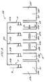
- FIG. 3 is a schematic side elevational view of a vertical cleaner 39 (i.e., a cleaner that supports substrates in a vertical orientation). After a substrate S is polished by a polisher (not shown) that supports substrates in a horizontal orientation, the substrate S enters the vertical cleaner 39 to be cleaned and optionally dried.
- the vertical cleaner 39 may comprise a plurality of cleaning modules 41, each cleaning module 41 having a substrate support 43a-d that may support a vertically oriented substrate S.
- the cleaning modules 41 may include a megasonic cleaner module 45, a pair of scrubber modules 47a-b, and a spin-rinse-dryer module 49.
- the vertical cleaner 39 also may optionally comprise an input module 51 and an output module 53. Both the input module 51 and the output module 53 may have a substrate support 43e, 43f, respectively, that supports a substrate in a horizontal orientation.
- a substrate transfer mechanism 55 having a plurality of substrate handlers 57a-e, is movably coupled above the modules 43-53.
- the substrate handlers 57a-e are positioned to selectively place and extract a substrate to and from the substrate supports 43a-f upon actuation of the substrate transfer mechanism 55.
- the substrate handlers 57a, 57e which place and extract substrates to and from the input module 51 and the output module 53, respectively, may comprise the inventive gripper/orienter assembly 11.
- the substrate transfer mechanism 55 is adapted to lift, lower, and to index horizontally forward and backward so as to transfer substrates between the input module 51, the cleaning modules 41, and the output module 53.
- the substrate transfer mechanism 55 may comprise an overhead walking beam-type robot, and the vertical cleaner 39 may be configured as described in U.S. Patent Application Serial No. 09/558,815, filed April 26, 2000 (AMAT No. 3156/CMP/RKK) the entire disclosure of which is incorporated herein by this reference.
- a horizontally oriented substrate S (e.g., which may have been extracted from a "horizontal” polisher) is loaded onto the horizontal substrate support 43e of the input module 51.
- the substrate handler 57a of the cleaner 39 Upon actuation of the inventive gripper/orienter assembly 11, the substrate handler 57a of the cleaner 39 then assumes the horizontal position (as shown in FIG. 1A) as described previously. Thereafter, the grippers 15a, 15b of the substrate handler 57a move away from each other.
- the gripper fingers 13a, 13b coupled to the grippers 15a, 15b move away from each other and the end effector 19a, 19b coupled to the gripper fingers 13a, 13b also move away from each other so as to position the gripper orienter assembly 11 of the substrate handler 57a in an open position (e.g., the distance between the end effectors 19a, 19b is slightly greater than the length of the horizontally oriented substrate S).
- the substrate handler 57a Upon actuation of the substrate transfer mechanism 55, the substrate handler 57a lowers so as to position the "open" end effectors 19a, 19b adjacent the edges of the horizontally oriented substrate S positioned on the substrate support 43e. Thereafter the grippers 15a, 15b, the gripper fingers 13a, 13b, and the end effectors 19a, 19b move toward each other, so as to position the substrate handler 57a in a closed position (e.g., the distance between the end effectors 19a, 19b is equal to the length of the horizontally oriented substrate S). In the closed position, the substrate handler 57a grasps the horizontally oriented substrate S. Thereafter, the substrate handler 57a, which includes the inventive gripper/orienter assembly 11, re-orients the substrate S from the horizontal position to the vertical position as described below.
- a closed position e.g., the distance between the end effectors 19a, 19b is equal to the length of the horizontally oriented substrate S.
- the rod 25 (FIGS. 1B, 2B) of the actuator 23 retracts so as to move the second lever 23 upward.
- the second lever 23 moves upward it causes the first lever 21, which is coupled to the second lever 23, to rotate counterclockwise about its central axis of rotation from the extended position, as shown in FIG. 2B, to the retracted position as shown in FIG. 1B.
- the pivot 27, which is fixedly coupled to the first lever 21 also rotates counterclockwise.
- the first end effector 19a which is coupled to the pivot 27, and the substrate S which is supported in part by the first end effector 19a, rotate to the vertical position as shown in FIG. 1A.
- the second end effector 19b rotates therewith via the bearing 20, to the vertical position as shown in FIG. 1A.
- the first substrate handler 57a may elevate upon actuation of the substrate transfer mechanism 55, thereby extracting the substrate S from the input module 51, and may index (i.e., move horizontally) to position the substrate S above the megasonic cleaner module 45. Thereafter, the first substrate handler 57a lowers the vertically oriented substrate S into the megasonic cleaner module 45 and places the substrate S on the substrate support 43a. The substrate S is then megasonically cleaned in the DI water bath as is conventionally known.
- the second substrate handler 57b extracts the substrate S and transfers the substrate S to the first scrubber module 47a for scrubbing, and, thereafter, the third substrate handler 57c transfers the substrate S to the second scrubber module 47b for scrubbing.
- DI water is sprayed on the substrate S while the scrubber brushes scrub the surface of the substrate S, as is conventionally known.
- the fourth substrate handler 57d extracts the vertically-oriented substrate S and transfers the substrate S to the spin-rinse-dryer module 49.
- the substrate S is rotated at high speed (e.g., 900 RPM) while DI water is sprayed onto the substrate S. After the substrate S is sufficiently rinsed, the DI water spray is turned off and the substrate S is spin-dried.
- the fifth substrate handler 57e which comprises the inventive gripper orienter assembly 11 of FIGS. 1A-2B, extracts the vertically oriented substrate S from the spin-rinse-dryer module 79, horizontally orients the substrate S as previously described, and places the substrate S on the horizontal substrate support 43f of the output module 53. Thereafter the substrate S may be extracted from the vertical cleaner 39 by a substrate handler that handles horizontally oriented substrates, as most conventional FAB's transport substrates in a horizontal orientation.
- the substrate S may be re-oriented between the horizontal position and the vertical position as the substrate S is moved through the vertical cleaner 39 (e.g., as the substrate moves between the input or output module and the cleaning modules).
- previously non-value added wafer transport time e.g., to or from a stand alone re-orienter
- the inventive gripper/orienter assembly 11 may increase wafer throughput.
- the invention may be employed with both pocket type and clamp type gripper assemblies (exemplary grippers are described in commonly assigned U.S. Patent Application Serial No. 09/559,889, filed April 26, 2000 (AMAT No. 3554/CMP/RKK) which is incorporated herein in its entirety by this reference.
Landscapes
- Engineering & Computer Science (AREA)
- Robotics (AREA)
- Mechanical Engineering (AREA)
- Container, Conveyance, Adherence, Positioning, Of Wafer (AREA)
Applications Claiming Priority (2)
| Application Number | Priority Date | Filing Date | Title |
|---|---|---|---|
| US14323299P | 1999-07-10 | 1999-07-10 | |
| US143232P | 1999-07-10 |
Publications (1)
| Publication Number | Publication Date |
|---|---|
| EP1068936A1 true EP1068936A1 (de) | 2001-01-17 |
Family
ID=22503173
Family Applications (1)
| Application Number | Title | Priority Date | Filing Date |
|---|---|---|---|
| EP00305703A Withdrawn EP1068936A1 (de) | 1999-07-10 | 2000-07-06 | Greifer mit Orientierungssystem für eine Halbleiterscheibe |
Country Status (2)
| Country | Link |
|---|---|
| EP (1) | EP1068936A1 (de) |
| JP (1) | JP2001035909A (de) |
Cited By (7)
| Publication number | Priority date | Publication date | Assignee | Title |
|---|---|---|---|---|
| WO2003007342A3 (en) * | 2001-07-13 | 2003-10-09 | Tru Si Technologies Inc | Alignment of semiconductor wafers and other articles |
| WO2004090948A1 (en) * | 2003-04-03 | 2004-10-21 | Applied Materials Inc. | Methods and apparatus for vertical transfer of semiconductor substrates between cleaning modules |
| WO2006124472A3 (en) * | 2005-05-12 | 2007-03-08 | Applied Materials Inc | Method and apparatus for vertical transfer of semiconductor substrates in a cleaning module |
| CN100426457C (zh) * | 2005-08-19 | 2008-10-15 | 大日本网目版制造株式会社 | 衬底处理设备和衬底处理方法 |
| CN110310911A (zh) * | 2019-06-26 | 2019-10-08 | 德淮半导体有限公司 | 半导体设备、晶圆传送机构及作业方法 |
| US20210407824A1 (en) * | 2020-06-30 | 2021-12-30 | Applied Materials, Inc. | Spm processing of substrates |
| CN115443529A (zh) * | 2020-07-01 | 2022-12-06 | 应用材料公司 | 用于材料沉积的设备、基板处理系统和基板处理的方法 |
Families Citing this family (2)
| Publication number | Priority date | Publication date | Assignee | Title |
|---|---|---|---|---|
| CN1317753C (zh) * | 2002-11-25 | 2007-05-23 | 宇东电浆科技股份有限公司 | 封装晶片的夹持装置 |
| KR101517690B1 (ko) | 2013-10-08 | 2015-05-04 | 주식회사 엘지실트론 | 웨이퍼 이송 장치 |
Citations (3)
| Publication number | Priority date | Publication date | Assignee | Title |
|---|---|---|---|---|
| JPH02106296A (ja) * | 1988-10-14 | 1990-04-18 | Seiko Instr Inc | 姿勢変換機構を有するハンドリング装置 |
| JPH0555342A (ja) * | 1991-08-26 | 1993-03-05 | Hitachi Ltd | ウエーハチヤツクおよびウエーハ搬送装置 |
| JPH05293785A (ja) * | 1992-04-17 | 1993-11-09 | Komatsu Denshi Kinzoku Kk | 半導体結晶棒把持装置および搬送装置 |
-
2000
- 2000-07-06 EP EP00305703A patent/EP1068936A1/de not_active Withdrawn
- 2000-07-10 JP JP2000208523A patent/JP2001035909A/ja not_active Withdrawn
Patent Citations (3)
| Publication number | Priority date | Publication date | Assignee | Title |
|---|---|---|---|---|
| JPH02106296A (ja) * | 1988-10-14 | 1990-04-18 | Seiko Instr Inc | 姿勢変換機構を有するハンドリング装置 |
| JPH0555342A (ja) * | 1991-08-26 | 1993-03-05 | Hitachi Ltd | ウエーハチヤツクおよびウエーハ搬送装置 |
| JPH05293785A (ja) * | 1992-04-17 | 1993-11-09 | Komatsu Denshi Kinzoku Kk | 半導体結晶棒把持装置および搬送装置 |
Non-Patent Citations (3)
| Title |
|---|
| PATENT ABSTRACTS OF JAPAN vol. 014, no. 315 (M - 0995) 6 July 1990 (1990-07-06) * |
| PATENT ABSTRACTS OF JAPAN vol. 017, no. 356 (E - 1394) 6 July 1993 (1993-07-06) * |
| PATENT ABSTRACTS OF JAPAN vol. 018, no. 079 (M - 1557) 9 February 1994 (1994-02-09) * |
Cited By (15)
| Publication number | Priority date | Publication date | Assignee | Title |
|---|---|---|---|---|
| US7052229B2 (en) | 2001-07-13 | 2006-05-30 | Tru-Si Technologies Inc. | Alignment of semiconductor wafers and other articles |
| WO2003007342A3 (en) * | 2001-07-13 | 2003-10-09 | Tru Si Technologies Inc | Alignment of semiconductor wafers and other articles |
| US6935830B2 (en) | 2001-07-13 | 2005-08-30 | Tru-Si Technologies, Inc. | Alignment of semiconductor wafers and other articles |
| US6948898B2 (en) | 2001-07-13 | 2005-09-27 | Tru-Si Technologies, Inc. | Alignment of semiconductor wafers and other articles |
| CN100397563C (zh) * | 2003-04-03 | 2008-06-25 | 应用材料股份有限公司 | 在清洁模块之间垂直传送半导体基板的方法和设备 |
| WO2004090948A1 (en) * | 2003-04-03 | 2004-10-21 | Applied Materials Inc. | Methods and apparatus for vertical transfer of semiconductor substrates between cleaning modules |
| WO2006124472A3 (en) * | 2005-05-12 | 2007-03-08 | Applied Materials Inc | Method and apparatus for vertical transfer of semiconductor substrates in a cleaning module |
| CN101409226B (zh) * | 2005-05-12 | 2011-03-30 | 应用材料股份有限公司 | 用于在清洁模块中垂直转移半导体基材的方法及设备 |
| CN100426457C (zh) * | 2005-08-19 | 2008-10-15 | 大日本网目版制造株式会社 | 衬底处理设备和衬底处理方法 |
| US7541285B2 (en) | 2005-08-19 | 2009-06-02 | Dainippon Screen Mfg. Co., Ltd. | Substrate processing apparatus and substrate processing method |
| CN110310911A (zh) * | 2019-06-26 | 2019-10-08 | 德淮半导体有限公司 | 半导体设备、晶圆传送机构及作业方法 |
| US20210407824A1 (en) * | 2020-06-30 | 2021-12-30 | Applied Materials, Inc. | Spm processing of substrates |
| CN115053333A (zh) * | 2020-06-30 | 2022-09-13 | 应用材料公司 | 基板的spm处理 |
| US12051599B2 (en) | 2020-06-30 | 2024-07-30 | Applied Materials, Inc. | Cleaning method with in-line SPM processing |
| CN115443529A (zh) * | 2020-07-01 | 2022-12-06 | 应用材料公司 | 用于材料沉积的设备、基板处理系统和基板处理的方法 |
Also Published As
| Publication number | Publication date |
|---|---|
| JP2001035909A (ja) | 2001-02-09 |
Similar Documents
| Publication | Publication Date | Title |
|---|---|---|
| KR102379269B1 (ko) | 통합된 얼라이너를 갖는 로봇 | |
| EP0858866B1 (de) | Mechanisches Greifergelenk für Roboter | |
| US6361422B1 (en) | Method and apparatus for transferring semiconductor substrates using an input module | |
| TWI773943B (zh) | 晶圓傳輸機械手及其晶圓翻轉方法 | |
| US8322963B2 (en) | End effector for a cluster tool | |
| US11908720B2 (en) | CMP wafer cleaning equipment, wafer transfer robot and wafer flipping method | |
| TWI654714B (zh) | Robot unit and transfer method | |
| US20090025749A1 (en) | Method for vertical transfer of semiconductor substrates in a cleaning module | |
| US7059944B2 (en) | Integrated system for processing semiconductor wafers | |
| US9327918B2 (en) | Substrate processing apparatus and substrate processing method for performing cleaning process and the like on substrate | |
| US7743449B2 (en) | System and method for a combined contact and non-contact wafer cleaning module | |
| CN110039441A (zh) | 一种化学机械平坦化设备 | |
| US6406359B1 (en) | Apparatus for transferring semiconductor substrates using an input module | |
| US20090061739A1 (en) | Polishing apparatus and method for polishing semiconductor wafers using load-unload stations | |
| JP2001035909A (ja) | ウェーハの向きを変えることができるグリッパ | |
| JP2013151034A (ja) | ロボットシステム | |
| US7007333B1 (en) | System and method for a combined contact and non-contact wafer cleaning module | |
| US20240100714A1 (en) | Method and apparatus for processing a substrate in cleaning modules | |
| JPS63137448A (ja) | 半導体ウエハ処理装置 | |
| WO2003068421A2 (en) | Integrated system for processing semiconductor wafers | |
| JP2000260857A (ja) | ウェハ搬送ロボットを用いたウェハ受渡し方法、及び、ウェハ処理装置 | |
| KR20240163492A (ko) | 기판 처리 장치 | |
| KR100316606B1 (ko) | 반도체 웨이퍼 핸들러 | |
| JPH11145092A (ja) | ウェットキャリアレス洗浄装置 | |
| JPS59102580A (ja) | ロボツトハンド |
Legal Events
| Date | Code | Title | Description |
|---|---|---|---|
| PUAI | Public reference made under article 153(3) epc to a published international application that has entered the european phase |
Free format text: ORIGINAL CODE: 0009012 |
|
| AK | Designated contracting states |
Kind code of ref document: A1 Designated state(s): DE FR GB IT NL |
|
| AX | Request for extension of the european patent |
Free format text: AL;LT;LV;MK;RO;SI |
|
| 17P | Request for examination filed |
Effective date: 20010716 |
|
| AKX | Designation fees paid |
Free format text: DE FR GB IT NL |
|
| STAA | Information on the status of an ep patent application or granted ep patent |
Free format text: STATUS: THE APPLICATION IS DEEMED TO BE WITHDRAWN |
|
| 18D | Application deemed to be withdrawn |
Effective date: 20030201 |