EP1071008B1 - Verfahren zur Durchführung einer Multiplikation mit Akkumulation in einem Galois-Feld - Google Patents
Verfahren zur Durchführung einer Multiplikation mit Akkumulation in einem Galois-Feld Download PDFInfo
- Publication number
- EP1071008B1 EP1071008B1 EP00401776A EP00401776A EP1071008B1 EP 1071008 B1 EP1071008 B1 EP 1071008B1 EP 00401776 A EP00401776 A EP 00401776A EP 00401776 A EP00401776 A EP 00401776A EP 1071008 B1 EP1071008 B1 EP 1071008B1
- Authority
- EP
- European Patent Office
- Prior art keywords
- bits
- multiplication
- register
- data item
- data
- Prior art date
- Legal status (The legal status is an assumption and is not a legal conclusion. Google has not performed a legal analysis and makes no representation as to the accuracy of the status listed.)
- Expired - Lifetime
Links
Images
Classifications
-
- G—PHYSICS
- G06—COMPUTING OR CALCULATING; COUNTING
- G06F—ELECTRIC DIGITAL DATA PROCESSING
- G06F7/00—Methods or arrangements for processing data by operating upon the order or content of the data handled
- G06F7/60—Methods or arrangements for performing computations using a digital non-denominational number representation, i.e. number representation without radix; Computing devices using combinations of denominational and non-denominational quantity representations, e.g. using difunction pulse trains, STEELE computers, phase computers
- G06F7/72—Methods or arrangements for performing computations using a digital non-denominational number representation, i.e. number representation without radix; Computing devices using combinations of denominational and non-denominational quantity representations, e.g. using difunction pulse trains, STEELE computers, phase computers using residue arithmetic
- G06F7/724—Finite field arithmetic
Definitions
- the invention relates to a method for effecting multiplication with accumulation in a Galois body. More particularly, the invention relates to a method for effecting multiplication with accumulation in a Galois body GF (2 k ).
- GF (2 k ) is the body of polynomials of degree at most k-1 with coefficients on ⁇ 0,1 ⁇ .
- Galois bodies are finite sets of elements on which mathematical operations are defined differently.
- Galois bodies are used in transmission digital to make either correcting codes of errors, either as a mathematical structure serving as support for the implementation of a cryptography.
- encryption codes we can cite the so-called elliptical curve encryption. This kind of encryption uses binary numbers encoded on a large number of bits (conventionally 150 to 200 bits).
- the means of calculation used at present are conventional processors, possibly coupled with dedicated circuits. If we use a processor classic, computing time is difficult optimized. On the other hand, the use of dedicated circuits is larger and uses more energy.
- an electronic circuit making it possible to carry out the multiplication in the sense of the arithmetic of the Galois body notably includes n accumulation flip-flops, n adders ...
- the size of the circuits making it possible to performing operations in the Galois body depends directly on the size in terms of the number of bits of the numbers involved in the different operations.
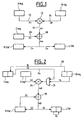
- Figure 1 shows a block diagram showing the conduct of a multiplication operation with accumulation in a Galois body according to the state of the technical.
- three data A B and C are involved.
- the first data A is stored in a first input register Areg
- the second datum B is stored in a second input register Breg
- the third datum C is stored in a third input register Creg.
- the data A, B and C have a size of 2 n bit.
- the first, second and third input register, respectively Areg Breg and Creg are preferably registers can contain 2 n bits. They can however have a different size, the size of these registers should however be sufficiently large to contain data A, B and C.
- the different registers can belong to a memory unit common or to different memory units.
- a multiplication circuit 10 in a body of Galois accepts as input the data A and B which are respectively transmitted by a first data bus 12 and by a second data bus 14 from the Areg and Breg input registers.
- the circuit of multiplication in the body of Galois 10 performs a multiplication according to the arithmetic of the Galois Body between the first datum A and the second datum B. De such circuits are known in the state of the art.
- the result of this multiplication, available in output from multiplication circuit 10, is a number coded on 4 n bits. This result is transmitted by means from a third data bus 16 to a circuit logic 18.
- Logic circuit 18 is used to perform the addition according to the arithmetic of the Body of Galois between the result of the multiplication in the body of Galois and the data C contained in the third Creg register.
- a third data bus 20 transmits the 2 n bits coding the number C to the circuit logic 18.
- logic circuit 18 is a "or exclusive" door with two entrances.
- the result of the addition in the sense of the arithmetic of the Galois body carried out by the logic circuit 18 is a number coded on 4 n bits.
- the 2 n least significant bits of the result of the addition operation are stored in a first output register LSW (Less Meaning Word in English literature) and the 2 n most significant bits of the result of the operation are stored in a second output register MSW (Most Significant Word in English literature).
- the size of the multiplication circuit 10 in the Galois body directly depends on the size of the numbers it has to multiply. However it is frequent, for example for so-called curve encryption calculation operations elliptical, having to perform multiplications between 32-bit numbers. The size of the multiplication circuit 10 is then very important and the implementation of such an operation becomes too expensive due to the size of the circuit multiplication.
- the purpose of the present invention is to provide a method for performing a type operation multiplication with accumulation in a body of Galois involving a multiplication circuit which is not penalizing in terms of size, and therefore high cost.
- the most significant bits of the second data are transferred to a target registry. Bits most significant of the second datum are then directly accessible for the second multiplication involved in the process according to the invention since the target register at the output of a two-way multiplexer inputs which receive the weight bits respectively weak from the second input register and the data from the target registry.
- the logic circuit used to realize additions in the Body of Galois is a door "or exclusive" with two entries.
- Figure 2 shows some similar elements to elements presented during the description of the figure 1. These common elements will be designated by same references.
- Figure 2 shows a first Areg input register and a second input register Breg, intended to receive respectively a first data A and a second data B coded on 32 bits.
- the numbers associated with different buses correspond to the numbers of bits set clearance for each corresponding operation.
- a bus from data 30 connects the second Breg register to the target register Treg.
- a multiplexer 31 receives at its two inputs a part of the bits from the target register Treg and other share of data from the second input register Breg.
- the output of the multiplexer 31 is connected to a multiplication circuit 34 which performs multiplications in the sense of the arithmetic of the body of Galois.
- the multiplication circuit 34 admits to a second entry the data from the first register Areg.
- a logic circuit 18 admits to a first input the data from the multiplication circuit 34 and at a second entry of data from a register MSW intermediary. Data from the circuit logic 18 are distributed between the MSW register and a LSW output register.
- the method according to the invention is implemented from the following way: the three data A, B and C are respectively stored in the first register input Areg, in the second input register Breg, and in the intermediate register MSW.
- a first step the 32 bits of the first data A are multiplied within the circuit of multiplication 34 by the 16 least significant bits of the second datum B. Simultaneously, the 16 bits of weight strong of the second datum B are transferred to the means from the data bus 30 to the least significant bits of the target register Treg.
- the result of multiplication performed between the 32 bits of the first data A and the 16 least significant bits of the second datum B provides a first intermediate result coded out of 48 bits.
- the logic circuit 18 allows an addition within the meaning of Galois arithmetic between the first result intermediate and the third datum C stored in the MSW intermediate register.
- a second intermediate result coded on 48 bits in logic circuit 18 output The 32 most significant bits of the second intermediate result are stored in the MSW intermediate register, while the 16 bits of low weight of the second intermediate result are stored in the LSW output register.
- 16 least significant bits of the second result are automatically stored in the 16 most significant bits of the LSW output register.
- a third step the 16 bits of weight low of the second intermediate result are shifted to the least significant bits of the output register LSW.
- a fourth step the 32 bits of the first data A are multiplied by the 16 bits of most significant of the second datum B within the circuit multiplication 34.
- a third result intermediate coded on 48 bits is thus obtained in output from the multiplication circuit 34.
- the third result intermediate is added within the logic circuit 18 to the content of the intermediate register MSW coded on 32 bits.
- a fourth intermediate result coded out of 48 bits is thus obtained at the output of logic circuit 18.
- the most significant 32 bits of this fourth intermediate result are stored in the MSW intermediate register and the 16 weight bits low of the fourth intermediate outcome are stored in the most significant bits of the LSW register.
- the most significant 16 bits of the second data B are transmitted to the circuit of multiplication 34 via an additional data bus 36 which connects the target register Treg and an entry of the multiplexer 31, and via multiplexer 31.
- Interest to do so is as follows: the 16 bits of weight strong of the second datum B being memorized in the 16 least significant bits of the Treg register, they are directly accessible by the circuit of multiplication 34.
- 16 most significant bits of the second data B directly from the second Breg register one or more cycle (s) of a clock governing the different operations would be required before the circuit multiplication 34 does actually access the 16 bits of most significant of the second datum B contained in the second Breg register.
- the method according to the invention can nevertheless operate without the intervention of the Treg register but performing multiplication with accumulation according to the process of the invention is then slower for the reasons just explained.
- the registers areg, Breg, Treg, MSW and LSW are preferably registers that can contain 32 bits. They may however be of a larger size.
- the data which are successively written in the MSW intermediate register erase data of this register.
- the method according to the invention can also be set up for the realization of a simple multiplication in the arithmetic sense of Galois. Indeed, a simple multiplication corresponds in the case of multiplication with accumulation where the data C is zero.
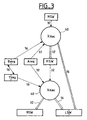
- FIG. 3 highlights the chain of two multiplication operations with accumulation that implements the method according to the invention to achieve the same result of multiplication with accumulation that can offer the prior art.
- the circles 40 represent electronic circuits making it possible to carry out multiplication operations with accumulation where one of the two factors of the multiplication is coded on 16 bits, the other factor of the multiplication is coded on 32 bits and where the added data is coded on 32 bits.
- the data A, B and C are initially stored in the registers Areg Breg and MSW.
- arrows in lines full from different registers and which are geared towards multiplication operations with accumulation indicate that data from these registers will be multiplied within the operation of multiplication with accumulation. Data from registers from which dotted arrows start will be added up within the operation of multiplication with accumulation. The double arrows from multiplication operations with accumulation are the results from these operations multiplication with accumulation.
- the arrows bidirectional indicate data exchange between two registers. The numbers associated with the different arrows correspond to the number of bits involved for each corresponding operation.
- the 32 bits of the first data A are multiplied to the 16 least significant bits of the second datum B, the result of this multiplication being added to 32 bits of data C to provide a result stored in the intermediate register MSW for the 32 most significant bits and in the LSW output register for the least significant 16 bits.
- the second operation multiplication with accumulation brought into play done intervene the 32 bits of data A, multiplied by the 16 most significant bits of the data B which have been previously transferred to the Treg target register, as well as the 32 new bits of the MSW register which involved in the addition of the operation of multiplication with accumulation.
- the result of the second multiplication with accumulation is memorized in the intermediate MSW register for the 32 bits of most significant, and in the most significant 16 bits of the LSW intermediate register for the 16 weight bits low.
- the final result of the Xmac operation (A, B, C) is the concatenation of the contents of the MSW register, of the 16 most significant bits of the LSW register and the 16 bits of low weight of the LSW register from the first multiplication operation with accumulation.
- the method according to the invention makes it possible to carry out an operation of multiplication with accumulation in the body of Galois between numbers coded on 2 n bits by proposing a clever sequence of identical operations, and in particular two multiplications between a number coded on 2 n bits and a number coded on n bits, which allows to have less bulky multiplier circuits.
Landscapes
- Physics & Mathematics (AREA)
- Engineering & Computer Science (AREA)
- General Physics & Mathematics (AREA)
- Mathematical Analysis (AREA)
- Mathematical Optimization (AREA)
- Pure & Applied Mathematics (AREA)
- Computational Mathematics (AREA)
- Theoretical Computer Science (AREA)
- Computing Systems (AREA)
- Mathematical Physics (AREA)
- General Engineering & Computer Science (AREA)
- Error Detection And Correction (AREA)
- Detection And Correction Of Errors (AREA)
Claims (5)
- Verfahren zur Durchführung einer Operation des Typs "Multiplikation mit Akkumulation" innerhalb eines Galois-Körpers, die auf ein erstes Datum, auf ein zweites Datum und auf ein drittes Datum innerhalb eines Galois-Körpers zugreifen kann, wobei jedes Datum mit 2 · n Bits kodiert ist, dadurch gekennzeichnet, daß es die Schritte umfaßt:Speichern des ersten Datums in einem ersten Eingangsregister, des zweiten Datums in einem zweiten Eingangsregister und des dritten Datums in einem Zwischenregister;Durchführen einer ersten Multiplikation des ersten Datums mit den n niedrigwertigen Bits des zweiten Datums mittels eines Multiplikationsschaltkreises und gemäß der Arithmetik des Galois-Körpers, um ein erstes Zwischenergebnis zu erhalten, das mit 3 · n Bits kodiert ist;Durchführen einer ersten Addition des dritten Datums und des ersten Zwischenergebnis mittels eines Logikschaltkreises und gemäß der Arithmetik des Galois-Körpers, um ein zweites Zwischenergebnis zu erhalten, das mit 3 · n Bits codiert ist;Speichern der 2 · n hochwertigen Bits des zweiten Zwischenergebnis in dem Zwischenregister und der n niedrigwertigen Bits des zweiten Zwischenergebnisses in einem Ausgangsregister;Verschieben der n niedrigwertigen in dem ersten Ausgangsspeicher gespeicherten Bits in die niedrigwertigen Bits des ersten Ausgangsregisters;Durchführen einer zweiten Multiplikation des ersten Datums mit den n hochwertigen Bits des zweiten Datums mittels des Multiplikationsschaltkreises und gemäß der Arithmetik des Galois-Körpers, um ein drittes Zwischenergebnis zu erhalten, das mit 3 · n Bits codiert ist;Durchführen einer zweiten Addition der 2 · n hochwertigen Bits des zweiten in dem Zwischenspeicher gespeicherten Zwischenergebnisses und des dritten Zwischenergebnis mittels des Logikschaltkreises und gemäß der Arithmetik des Galois-Körpers, um ein viertes Zwischenergebnis zu erhalten, das mit 3 · n Bits codiert ist;Speichern der 2 · n hochwertigen Bits des vierten Zwischenergebnis in dem Zwischenregister und der 2 · n niedrigwertigen Bits in dem Ausgangsregister.
- Verfahren nach Anspruch 1, dadurch gekennzeichnet, daß die hochwertigen Bits des zweiten Datums (B) in ein Zielregister (Treg) übertragen werden, wo diese über einen Datenbus (36) und einen Multiplexer (31) für die zweite Multiplikation zur Verfügung stehen.
- Verfahren nach einem der vorangegangenen Ansprüche, dadurch gekennzeichnet, daß das erste Datum (A), das zweite Datum (B) und das dritte Datum (C) mit 32 Bit kodiert sind.
- Verfahren nach einem der vorangegangenen Ansprüche, dadurch gekennzeichnet, daß der Logikschaltkreis (18), welcher die Durchführung der ersten und der zweiten Addition gestattet, ein XOR-Gatter (exklusiv-ODER) ist.
- Verfahren nach einem der vorangegangenen Ansprüche, dadurch gekennzeichnet, daß das dritte Datum (C) null ist.
Applications Claiming Priority (2)
| Application Number | Priority Date | Filing Date | Title |
|---|---|---|---|
| FR9909395A FR2796736B1 (fr) | 1999-07-20 | 1999-07-20 | Procede pour effectuer une multiplication avec accumulation dans un corps de galois |
| FR9909395 | 1999-07-20 |
Publications (2)
| Publication Number | Publication Date |
|---|---|
| EP1071008A1 EP1071008A1 (de) | 2001-01-24 |
| EP1071008B1 true EP1071008B1 (de) | 2003-08-13 |
Family
ID=9548302
Family Applications (1)
| Application Number | Title | Priority Date | Filing Date |
|---|---|---|---|
| EP00401776A Expired - Lifetime EP1071008B1 (de) | 1999-07-20 | 2000-06-22 | Verfahren zur Durchführung einer Multiplikation mit Akkumulation in einem Galois-Feld |
Country Status (4)
| Country | Link |
|---|---|
| US (1) | US6609142B1 (de) |
| EP (1) | EP1071008B1 (de) |
| DE (1) | DE60004449D1 (de) |
| FR (1) | FR2796736B1 (de) |
Families Citing this family (9)
| Publication number | Priority date | Publication date | Assignee | Title |
|---|---|---|---|---|
| US7177891B2 (en) | 2002-10-09 | 2007-02-13 | Analog Devices, Inc. | Compact Galois field multiplier engine |
| US7082452B2 (en) * | 2001-11-30 | 2006-07-25 | Analog Devices, Inc. | Galois field multiply/multiply-add/multiply accumulate |
| DE10164416A1 (de) * | 2001-12-29 | 2003-07-10 | Philips Intellectual Property | Verfahren zum Multiplizieren zweier Faktoren aus dem Galois-Feld sowie Multiplizierer zum Durchführen des Verfahrens |
| US9513906B2 (en) | 2013-01-23 | 2016-12-06 | International Business Machines Corporation | Vector checksum instruction |
| US9471308B2 (en) | 2013-01-23 | 2016-10-18 | International Business Machines Corporation | Vector floating point test data class immediate instruction |
| US9804840B2 (en) | 2013-01-23 | 2017-10-31 | International Business Machines Corporation | Vector Galois Field Multiply Sum and Accumulate instruction |
| US9823924B2 (en) | 2013-01-23 | 2017-11-21 | International Business Machines Corporation | Vector element rotate and insert under mask instruction |
| US9778932B2 (en) | 2013-01-23 | 2017-10-03 | International Business Machines Corporation | Vector generate mask instruction |
| US9715385B2 (en) | 2013-01-23 | 2017-07-25 | International Business Machines Corporation | Vector exception code |
Family Cites Families (9)
| Publication number | Priority date | Publication date | Assignee | Title |
|---|---|---|---|---|
| US4251875A (en) * | 1979-02-12 | 1981-02-17 | Sperry Corporation | Sequential Galois multiplication in GF(2n) with GF(2m) Galois multiplication gates |
| FR2605769B1 (fr) * | 1986-10-22 | 1988-12-09 | Thomson Csf | Operateur polynomial dans les corps de galois et processeur de traitement de signal numerique comportant un tel operateur |
| US5623683A (en) * | 1992-12-30 | 1997-04-22 | Intel Corporation | Two stage binary multiplier |
| KR970003979B1 (ko) * | 1993-11-29 | 1997-03-24 | 삼성전자 주식회사 | 갈로이스 필드상의 승산기 |
| US6470370B2 (en) * | 1995-09-05 | 2002-10-22 | Intel Corporation | Method and apparatus for multiplying and accumulating complex numbers in a digital filter |
| US5862067A (en) * | 1995-12-29 | 1999-01-19 | Intel Corporation | Method and apparatus for providing high numerical accuracy with packed multiply-add or multiply-subtract operations |
| US6317770B1 (en) * | 1997-08-30 | 2001-11-13 | Lg Electronics Inc. | High speed digital signal processor |
| US6078939A (en) * | 1997-09-30 | 2000-06-20 | Intel Corporation | Apparatus useful in floating point arithmetic |
| US6182104B1 (en) * | 1998-07-22 | 2001-01-30 | Motorola, Inc. | Circuit and method of modulo multiplication |
-
1999
- 1999-07-20 FR FR9909395A patent/FR2796736B1/fr not_active Expired - Fee Related
-
2000
- 2000-06-22 DE DE60004449T patent/DE60004449D1/de not_active Expired - Lifetime
- 2000-06-22 EP EP00401776A patent/EP1071008B1/de not_active Expired - Lifetime
- 2000-07-20 US US09/621,891 patent/US6609142B1/en not_active Expired - Lifetime
Also Published As
| Publication number | Publication date |
|---|---|
| EP1071008A1 (de) | 2001-01-24 |
| FR2796736B1 (fr) | 2001-11-30 |
| FR2796736A1 (fr) | 2001-01-26 |
| US6609142B1 (en) | 2003-08-19 |
| DE60004449D1 (de) | 2003-09-18 |
Similar Documents
| Publication | Publication Date | Title |
|---|---|---|
| EP0712071B1 (de) | Verfahren zur Verwendung der modularen Multiplikation nach der Montgomery-Methode | |
| EP0712072A1 (de) | Verfahren zur Ausführung von modularen Reduktion nach der Montgomery-Methode | |
| EP2515227B1 (de) | Multiplikationsschaltkreis nach Montgomery | |
| FR2867579A1 (fr) | Multiplieur modulaire de montgomery | |
| TWI263402B (en) | Reconfigurable fir filter | |
| EP1071008B1 (de) | Verfahren zur Durchführung einer Multiplikation mit Akkumulation in einem Galois-Feld | |
| EP0437876B1 (de) | Programmierbarer serieller Multiplikator | |
| EP0712070A1 (de) | Verfahren zum Erzeugen eines Fehlerkorrekturparameters in Verbindung mit der Verwendung von modularen Operationen nach der Montgomery-Methode | |
| EP0939362A1 (de) | Koprozessor für moduläre Arithmetik mit einer schnellen Ausführung von nicht-modulären Operationen | |
| EP0237382B1 (de) | Gerät zur Kosinustransformation eines abgetasteten digitalen Signals | |
| TWI240199B (en) | Interstitial product generator, multiplication circuit and multiplication method for bit segments | |
| EP0690584B1 (de) | Schaltung zur Ortung von Fehlern in einem Reed-Solomon Dekoder | |
| EP0778518B1 (de) | Verfahren zum Erzeugen eines Parameters J0 bezüglich der Verwendung von modularen Operationen nach der Montgomery-Methode | |
| EP0785502B1 (de) | Verfahren zum Erzeugen eines Fehlerkorrekturparameters bezüglich der Verwendung von modularen Operationen nach der Montgomery-Methode | |
| FR2773284A1 (fr) | Circuit de calcul de polynome de syndrome et un circuit de decodage reed-solomon | |
| EP0927928B1 (de) | Verbessertes Verfahren zum Erzeugen eines Parameters J0 bezüglich der Verwendung von modularen Operationen nach der Montgomery-Methode | |
| EP0947913B1 (de) | Verbessertes Verfahren zur Ausführung ganzzahliger Division | |
| EP0175623A1 (de) | Einrichtung zur Echtzeitdigitalsignalverarbeitung durch Faltung | |
| EP0784262B1 (de) | Einrichtung und Verfahren zur Verbesserung der Verarbeitungsgeschwindigkeit eines Koprozessors für moduläre Arithmetik | |
| EP1020792B1 (de) | Multiplizierschaltung die sowohl gewöhnliche, als auch Galoisfeld-Multiplikation ausführen kann | |
| FR2771525A1 (fr) | Procede de production d'un parametre de correction d'erreur associe a la mise en oeuvre d'operation modulaire selon la methode de montgomery | |
| EP0902359B1 (de) | Verfahren und Anordnung zur Durchführung ganzzahliger Divisionsoperationen mit einem modulo-arithmetischen Koprozessor | |
| EP0125156B1 (de) | Kaskadierter Multiplizierer mit einer Anordnung von elementären Operatoren | |
| FR2602073A1 (fr) | Circuit de traitement numerique de signal realisant une transformation cosinus. | |
| EP0613251A1 (de) | Frequenzteiler |
Legal Events
| Date | Code | Title | Description |
|---|---|---|---|
| PUAI | Public reference made under article 153(3) epc to a published international application that has entered the european phase |
Free format text: ORIGINAL CODE: 0009012 |
|
| AK | Designated contracting states |
Kind code of ref document: A1 Designated state(s): DE FR GB IT |
|
| AX | Request for extension of the european patent |
Free format text: AL;LT;LV;MK;RO;SI |
|
| 17P | Request for examination filed |
Effective date: 20010712 |
|
| AKX | Designation fees paid |
Free format text: DE FR GB IT |
|
| RAP1 | Party data changed (applicant data changed or rights of an application transferred) |
Owner name: STMICROELECTRONICS S.A. |
|
| GRAH | Despatch of communication of intention to grant a patent |
Free format text: ORIGINAL CODE: EPIDOS IGRA |
|
| GRAH | Despatch of communication of intention to grant a patent |
Free format text: ORIGINAL CODE: EPIDOS IGRA |
|
| GRAA | (expected) grant |
Free format text: ORIGINAL CODE: 0009210 |
|
| AK | Designated contracting states |
Designated state(s): DE FR GB IT |
|
| PG25 | Lapsed in a contracting state [announced via postgrant information from national office to epo] |
Ref country code: IT Free format text: LAPSE BECAUSE OF FAILURE TO SUBMIT A TRANSLATION OF THE DESCRIPTION OR TO PAY THE FEE WITHIN THE PRESCRIBED TIME-LIMIT;WARNING: LAPSES OF ITALIAN PATENTS WITH EFFECTIVE DATE BEFORE 2007 MAY HAVE OCCURRED AT ANY TIME BEFORE 2007. THE CORRECT EFFECTIVE DATE MAY BE DIFFERENT FROM THE ONE RECORDED. Effective date: 20030813 |
|
| REG | Reference to a national code |
Ref country code: GB Ref legal event code: FG4D Free format text: NOT ENGLISH |
|
| GBT | Gb: translation of ep patent filed (gb section 77(6)(a)/1977) | ||
| REF | Corresponds to: |
Ref document number: 60004449 Country of ref document: DE Date of ref document: 20030918 Kind code of ref document: P |
|
| PG25 | Lapsed in a contracting state [announced via postgrant information from national office to epo] |
Ref country code: DE Free format text: LAPSE BECAUSE OF FAILURE TO SUBMIT A TRANSLATION OF THE DESCRIPTION OR TO PAY THE FEE WITHIN THE PRESCRIBED TIME-LIMIT Effective date: 20031114 |
|
| PLBE | No opposition filed within time limit |
Free format text: ORIGINAL CODE: 0009261 |
|
| STAA | Information on the status of an ep patent application or granted ep patent |
Free format text: STATUS: NO OPPOSITION FILED WITHIN TIME LIMIT |
|
| 26N | No opposition filed |
Effective date: 20040514 |
|
| PGFP | Annual fee paid to national office [announced via postgrant information from national office to epo] |
Ref country code: GB Payment date: 20080527 Year of fee payment: 9 |
|
| GBPC | Gb: european patent ceased through non-payment of renewal fee |
Effective date: 20090622 |
|
| PG25 | Lapsed in a contracting state [announced via postgrant information from national office to epo] |
Ref country code: GB Free format text: LAPSE BECAUSE OF NON-PAYMENT OF DUE FEES Effective date: 20090622 |
|
| PGFP | Annual fee paid to national office [announced via postgrant information from national office to epo] |
Ref country code: FR Payment date: 20100729 Year of fee payment: 11 |
|
| REG | Reference to a national code |
Ref country code: FR Ref legal event code: ST Effective date: 20120229 |
|
| PG25 | Lapsed in a contracting state [announced via postgrant information from national office to epo] |
Ref country code: FR Free format text: LAPSE BECAUSE OF NON-PAYMENT OF DUE FEES Effective date: 20110630 |