EP1073090A2 - Dispositif d'affichage à émission de champ utilisant des nanotubes de carbone, et procédé de fabrication - Google Patents
Dispositif d'affichage à émission de champ utilisant des nanotubes de carbone, et procédé de fabrication Download PDFInfo
- Publication number
- EP1073090A2 EP1073090A2 EP00305791A EP00305791A EP1073090A2 EP 1073090 A2 EP1073090 A2 EP 1073090A2 EP 00305791 A EP00305791 A EP 00305791A EP 00305791 A EP00305791 A EP 00305791A EP 1073090 A2 EP1073090 A2 EP 1073090A2
- Authority
- EP
- European Patent Office
- Prior art keywords
- metal film
- fine holes
- carbon nanotubes
- field emission
- emission display
- Prior art date
- Legal status (The legal status is an assumption and is not a legal conclusion. Google has not performed a legal analysis and makes no representation as to the accuracy of the status listed.)
- Withdrawn
Links
Images

Classifications
-
- B—PERFORMING OPERATIONS; TRANSPORTING
- B82—NANOTECHNOLOGY
- B82Y—SPECIFIC USES OR APPLICATIONS OF NANOSTRUCTURES; MEASUREMENT OR ANALYSIS OF NANOSTRUCTURES; MANUFACTURE OR TREATMENT OF NANOSTRUCTURES
- B82Y10/00—Nanotechnology for information processing, storage or transmission, e.g. quantum computing or single electron logic
-
- H—ELECTRICITY
- H01—ELECTRIC ELEMENTS
- H01J—ELECTRIC DISCHARGE TUBES OR DISCHARGE LAMPS
- H01J31/00—Cathode ray tubes; Electron beam tubes
- H01J31/08—Cathode ray tubes; Electron beam tubes having a screen on or from which an image or pattern is formed, picked up, converted, or stored
- H01J31/10—Image or pattern display tubes, i.e. having electrical input and optical output; Flying-spot tubes for scanning purposes
- H01J31/12—Image or pattern display tubes, i.e. having electrical input and optical output; Flying-spot tubes for scanning purposes with luminescent screen
- H01J31/123—Flat display tubes
- H01J31/125—Flat display tubes provided with control means permitting the electron beam to reach selected parts of the screen, e.g. digital selection
- H01J31/127—Flat display tubes provided with control means permitting the electron beam to reach selected parts of the screen, e.g. digital selection using large area or array sources, i.e. essentially a source for each pixel group
-
- H—ELECTRICITY
- H01—ELECTRIC ELEMENTS
- H01J—ELECTRIC DISCHARGE TUBES OR DISCHARGE LAMPS
- H01J9/00—Apparatus or processes specially adapted for the manufacture, installation, removal, maintenance of electric discharge tubes, discharge lamps, or parts thereof; Recovery of material from discharge tubes or lamps
- H01J9/02—Manufacture of electrodes or electrode systems
- H01J9/022—Manufacture of electrodes or electrode systems of cold cathodes
- H01J9/025—Manufacture of electrodes or electrode systems of cold cathodes of field emission cathodes
-
- H—ELECTRICITY
- H01—ELECTRIC ELEMENTS
- H01J—ELECTRIC DISCHARGE TUBES OR DISCHARGE LAMPS
- H01J2201/00—Electrodes common to discharge tubes
- H01J2201/30—Cold cathodes
- H01J2201/304—Field emission cathodes
- H01J2201/30446—Field emission cathodes characterised by the emitter material
- H01J2201/30453—Carbon types
- H01J2201/30469—Carbon nanotubes (CNTs)
Definitions
- the present invention relates to a field emission display (FED) device and a manufacturing method thereof, and more particularly, to an FED device using carbon nanotubes and a manufacturing method thereof.
- FED field emission display
- FED field emission display
- Conventional carbon nanotubes are synthesized by an electrical discharge method or a laser deposition method, and put in a cleaning solution and shaken by an ultrasonic washer to be refined.
- the refined carbon nanotubes are implanted into the pores of a porous ceramic filter to apply the refined carbon nanotubes to an FED device.
- the carbon nanotubes contained in the pores of the porous ceramic filter are stamped and stood upright on conductive polymer on a lower substrate for an FED device, thereby forming emitter tips.
- the FED device using conventional carbon nanotubes as an emitter tip excels in stability compared to an FED device using silicon emitter tips.
- the FED device using conventional carbon nanotubes has difficulty in efficiently standing carbon nanotubes on the conductive polymer, and its manufacturing method is complicated.
- the FED device using conventional carbon nanotubes has a low manufacturing yield, and cannot be manufactured to have a large area.
- An objective of the present invention is to provide a field emission display (FED) device using carbon nanotubes, which can be manufactured to have a large area, and which has a high density of tips per unit area.
- FED field emission display
- Another objective of the present invention is to provide a method of manufacturing an FED device which can be manufactured to have a large area by a simple manufacturing process.
- the present invention provides a field emission display device including a first metal film for use as a cathode formed on a lower substrate; and a dielectric film pattern and a second metal film pattern formed on the first metal film, each of which has a plurality of fine holes which expose the first metal film.
- the lower substrate can be formed of glass, quartz, silicon or alumina (Al 2 O 3 ).
- the first metal film can be formed of chrome, titanium, tungsten or aluminum, and the second metal film pattern can be formed of chrome, titanium or palladium.
- Each of the fine holes can have a diameter of 0.5 to 10.0 ⁇ m.
- a conductive high polymer film is formed within the fine holes. Carbon nanotubes for use as emitter tips are vertically arranged within the conductive high polymer film.
- a spacer is installed on the second metal film pattern.
- An upper substrate, to which a transparent electrode and a fluorescent material are attached, is positioned on the spacer.
- the present invention provides a method of manufacturing a field emission display device.
- a first metal film for use as a cathode is formed on a lower substrate.
- a dielectric film is formed on the first metal film.
- a second metal film for use as a gate electrode is formed on the dielectric film.
- a dielectric film pattern and a second metal film pattern, each of which has a plurality of fine holes which expose the first metal film, are formed by patterning the second metal film and the dielectric film.
- a liquid conductive high polymer film is formed within the fine holes. Carbon nanotubes for use as emitter tips are sprayed into the fine holes and vertically arranged. Here, the carbon nanotubes are stood upright within the fine holes by ultrasonic vibration or voltage application.
- the liquid conductive high polymer film is cured, and then a spacer is installed on the second metal film pattern.
- An upper substrate, having a transparent electrode and a fluorescent material attached thereto, is attached to the spacer.
- An FED device using carbon nanotubes according to the present invention as described above can be simply manufactured to have a large area by a method of forming fine holes in a second metal film and a dielectric film and putting carbon nanotubes into the fine holes.
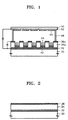
- a field emission display (FED) display using carbon nanotubes has a first metal film 32 for use as a cathode formed on a lower substrate 30.
- the lower substrate 30 is formed of glass quartz, silicon or alumina Al 2 O 3 .
- the first metal film 32 is formed of chrome, titanium, tungsten or aluminum.
- a dielectric film pattern 34a and a second metal film pattern 36a, each of which has a plurality of fine holes which expose the first metal film 32, are formed on the first metal film 32.
- the second metal film pattern 36a can be formed of chrome, titanium or palladium, and is used as a gate electrode in an FED device.
- the fine holes can be formed to have a diameter of 0.5 to 10.0 ⁇ m.
- a conductive high polymer film 42 is formed within the fine holes, and carbon nanotubes 44 are arranged vertically within the conductive high polymer film 42.
- the carbon nanotubes 44 are used as emitter tips. These vertically-arranged carbon nanotubes 44 can obtain a great amount of emission current at a low operating voltage, for example, about 1.5V/ ⁇ m. Also, the vertically-arranged carbon nanotubes 44 can increase luminous efficiency since they have a high density of tips per unit area.
- a spacer 48 is installed on the second metal film pattern 36a, and an upper substrate 50, to which a transparent electrode 52 for an anode and a fluorescent material 54 are attached, is provided on the spacer 48.
- the FED device according to the present invention is a three-electrode FED device.
- FIGS. 2 through 4 are cross-sectional views illustrating a method of manufacturing the FED display of FIG. 1.
- FIG. 2 illustrates the step of forming a first metal film 32, a dielectric film 34 and a second metal film 36 on a lower substrate 30.
- the first metal film 32 serving as a cathode is formed to a thickness of 0.2 to 0.5 ⁇ m on the wide lower substrate 30.
- the lower substrate 30 is formed of glass, quartz, silicon or alumina (Al 2 O 3 ).
- the first metal film 32 is formed of chrome, titanium, tungsten or aluminum.
- the dielectric film 34 is formed to a thickness of 1 to 5 ⁇ m on the first metal film at a low temperature.
- the second metal film 36 serving as a gate electrode is formed to a thickness of 0.2 to 0.5 ⁇ m on the dielectric film 34.
- the second metal film 36 is formed of chrome. titanium or palladium by an electron-beam deposition method or a thermal deposition method.
- FIG. 3 illustrates the step of forming a second metal film pattern 36a and a dielectric film pattern 34a, each of which has fine holes 40, by patterning the second metal film 36 and the dielectric film 34.
- the second metal film 36 is coated with a photoresist film (not shown) having a thickness of 1.5 to 2.0 ⁇ m, and the photoresist film is developed, thereby forming a photoresist pattern 38.
- the second metal film 36 and the dielectric film 34 are etched using the photoresist pattern 38 as a mask, thereby forming the second metal film pattern 36a and the dielectric film pattern 34a.
- a plurality of fine holes 40 are formed to expose the first metal film 32.
- the fine holes 40 each have a diameter of about 0.5 to 10.0 ⁇ m, and are separated from each other at intervals of about 2.0 to 15.0 ⁇ m.
- FIG. 4 illustrates the step of forming a conductive high polymer film 42 and positioning carbon nanotubes 44 within the fine holes 40.
- the conductive high polymer film 42 is formed by filling 1/3 of each of the fine holes 40 of the dielectric film 34 with liquid conductive high polymer.
- the conductive high polymer can be a carbon adhesive or a silver adhesive.
- carbon nanotubes 44 for use as emitter tips are sprayed into the fine holes 40 by ultrasonic vibration, voltage impression, or the like, and are vertically oriented on the first metal film 32.
- ultrasonic vibration is applied, a voltage is applied between the upper and lower portions of the lower substrate 30, or the two methods are both performed on the resultant structure.
- the carbon nanotubes are effectively injected and stood upright in the conductive high polymer film 42 within the fine holes 40.
- the carbon nanotubes 44 are vertically aligned in the conductive high polymer film 42 on the first metal film 32.
- the vertically-oriented carbon nanotubes 44 can obtain a great amount of emission current at a low operating voltage, for example, at about 1.5 V/ ⁇ m. Also, the vertically-oriented carbon nanotubes 44 provide excellent luminous efficiency since they have a high density of tips per unit area.
- the liquid conductive high polymer film 42 on which the carbon nanotubes 44 have been sprayed is cured at 400°C or less, preferably, at 300 to 400°C.
- a spacer 48 is installed to a length of about 100 to 700 ⁇ m on the second metal film pattern 36a.
- the transparent electrode 52 serving as an anode is formed on the upper substrate 50, and a fluorescent material 54, which emits light when bombarded by electrons, is then attached to the transparent electrode 52.
- a glass substrate is used as the upper substrate 50, and an indium tin oxide (ITO) electrode can be used as the transparent electrode.
- ITO indium tin oxide
- the upper substrate 50 to which the transparent electrode 52 and the fluorescent material 54 are attached is turned upside down and put on the spacer 48, and then vacuum is sealed and mounted, thereby completing the formation of the FED device.
- An FED device using carbon nanotubes according to the present invention as described above can be simply manufactured with a large area by a method of forming fine holes in a second metal film and a dielectric film, and putting carbon nanotube in the fine holes.
- the FED device according to the present invention can obtain a great amount of emission current at a low operating voltage, for example, at about 1.5V/ ⁇ m, since it uses carbon nanotubes which is vertically oriented well as emitter tips. Also, the FED device according to the present invention provides excellent luminous efficiency, high reliability, and high yield since it has a high density of tips per unit area.
Landscapes
- Engineering & Computer Science (AREA)
- Chemical & Material Sciences (AREA)
- Nanotechnology (AREA)
- Manufacturing & Machinery (AREA)
- Physics & Mathematics (AREA)
- Mathematical Physics (AREA)
- Theoretical Computer Science (AREA)
- Crystallography & Structural Chemistry (AREA)
- Cold Cathode And The Manufacture (AREA)
- Cathode-Ray Tubes And Fluorescent Screens For Display (AREA)
- Electrodes For Cathode-Ray Tubes (AREA)
Applications Claiming Priority (5)
| Application Number | Priority Date | Filing Date | Title |
|---|---|---|---|
| KR1019990030698A KR19990073591A (ko) | 1999-07-27 | 1999-07-27 | 미세구멍을 이용한 탄소나노튜브 3전극 에프이디의 제작. |
| KR9930698 | 1999-07-27 | ||
| KR1020000029579A KR20010029761A (ko) | 1999-07-27 | 2000-05-31 | 탄소 나노튜브를 이용한 전계방출 표시소자 및 그 제조 방법 |
| KR2000029579 | 2000-05-31 | ||
| KR0029579 | 2000-05-31 |
Publications (2)
| Publication Number | Publication Date |
|---|---|
| EP1073090A2 true EP1073090A2 (fr) | 2001-01-31 |
| EP1073090A3 EP1073090A3 (fr) | 2003-04-16 |
Family
ID=26635947
Family Applications (1)
| Application Number | Title | Priority Date | Filing Date |
|---|---|---|---|
| EP00305791A Withdrawn EP1073090A3 (fr) | 1999-07-27 | 2000-07-07 | Dispositif d'affichage à émission de champ utilisant des nanotubes de carbone, et procédé de fabrication |
Country Status (3)
| Country | Link |
|---|---|
| EP (1) | EP1073090A3 (fr) |
| JP (1) | JP2001076651A (fr) |
| CN (1) | CN1286500A (fr) |
Cited By (21)
| Publication number | Priority date | Publication date | Assignee | Title |
|---|---|---|---|---|
| FR2797520A1 (fr) * | 1999-08-10 | 2001-02-16 | Delta Optoelectronics Inc | Cellule lumineuse et procede d'emission de lumiere |
| GB2361805A (en) * | 2000-04-26 | 2001-10-31 | Samsung Sdi Co Ltd | Field emission array with carbon nanotubes and method of fabrication |
| EP1283541A3 (fr) * | 2001-08-06 | 2003-03-12 | Samsung SDI Co., Ltd. | Procédé de fabrication d'un dispositif d'affichage à émission de champ utilisant des nanotubes de carbone |
| WO2003021621A1 (fr) * | 2001-08-28 | 2003-03-13 | Motorola, Inc. | Dispositif d'emission electronique comprenant des nanotubes de carbone etires |
| EP1073085A3 (fr) * | 1999-07-29 | 2003-04-09 | Sony Corporation | Procédé de fabrication d'un émetteur de champ à cathode froide et d'un dispositif d'affichage |
| US6700454B2 (en) | 2001-06-29 | 2004-03-02 | Zvi Yaniv | Integrated RF array using carbon nanotube cathodes |
| US6739932B2 (en) | 2001-06-07 | 2004-05-25 | Si Diamond Technology, Inc. | Field emission display using carbon nanotubes and methods of making the same |
| US6897603B2 (en) | 2001-08-24 | 2005-05-24 | Si Diamond Technology, Inc. | Catalyst for carbon nanotube growth |
| US6911767B2 (en) | 2001-06-14 | 2005-06-28 | Hyperion Catalysis International, Inc. | Field emission devices using ion bombarded carbon nanotubes |
| US6979947B2 (en) | 2002-07-09 | 2005-12-27 | Si Diamond Technology, Inc. | Nanotriode utilizing carbon nanotubes and fibers |
| EP1329928A3 (fr) * | 2001-12-20 | 2006-02-08 | Ngk Insulators, Ltd. | Element d'émission d'électrons et affichage à émission par effet de champ l'utilisant |
| US7026432B2 (en) | 2003-08-12 | 2006-04-11 | General Electric Company | Electrically conductive compositions and method of manufacture thereof |
| US7088049B2 (en) | 2000-12-22 | 2006-08-08 | Ngk Insulators, Ltd. | Electron-emitting device and field emission display using the same |
| US7309727B2 (en) | 2003-09-29 | 2007-12-18 | General Electric Company | Conductive thermoplastic compositions, methods of manufacture and articles derived from such compositions |
| US7341498B2 (en) | 2001-06-14 | 2008-03-11 | Hyperion Catalysis International, Inc. | Method of irradiating field emission cathode having nanotubes |
| US7354988B2 (en) | 2003-08-12 | 2008-04-08 | General Electric Company | Electrically conductive compositions and method of manufacture thereof |
| CN100399496C (zh) * | 2003-08-05 | 2008-07-02 | 东南大学 | 一种场致发射显示板及其驱动方法 |
| US7462656B2 (en) | 2005-02-15 | 2008-12-09 | Sabic Innovative Plastics Ip B.V. | Electrically conductive compositions and method of manufacture thereof |
| US7601043B2 (en) | 2003-01-15 | 2009-10-13 | Postech Foundation | Method of manufacturing microholes in a cathode substrate of a field emission display using anodic oxidation |
| US7960904B2 (en) | 2001-06-14 | 2011-06-14 | Hyperion Catalysis International, Inc. | Field emission devices using carbon nanotubes modified by energy, plasma, chemical or mechanical treatment |
| US10141154B2 (en) | 2015-05-13 | 2018-11-27 | Boe Technology Group Co., Ltd. | Array substrate, display panel and display apparatus having the same, and fabricating method thereof |
Families Citing this family (9)
| Publication number | Priority date | Publication date | Assignee | Title |
|---|---|---|---|---|
| JP3494583B2 (ja) * | 1999-01-13 | 2004-02-09 | 松下電器産業株式会社 | 電子放出素子の製造方法 |
| KR20040030553A (ko) * | 2001-03-26 | 2004-04-09 | 에이코스 인코포레이티드 | 탄소 나노튜브를 함유하는 코팅막 |
| JP2003168355A (ja) * | 2001-11-30 | 2003-06-13 | Sony Corp | 電子放出体の製造方法、冷陰極電界電子放出素子の製造方法、並びに、冷陰極電界電子放出表示装置の製造方法 |
| JP3839713B2 (ja) | 2001-12-12 | 2006-11-01 | 株式会社ノリタケカンパニーリミテド | 平面ディスプレイの製造方法 |
| AU2003281237A1 (en) * | 2002-07-03 | 2004-01-23 | Applied Nanotechnologies, Inc. | Fabrication and activation processes for nanostructure composite field emission cathodes |
| CN1321885C (zh) * | 2003-01-23 | 2007-06-20 | 南昌大学 | 在软基底上制造定向碳纳米管膜方法 |
| CN100437876C (zh) * | 2003-03-27 | 2008-11-26 | 清华大学 | 一种场发射元件 |
| CN100391313C (zh) * | 2004-07-08 | 2008-05-28 | 东元奈米应材股份有限公司 | 场发射显示器的阴极结构制作方法 |
| CN100543905C (zh) | 2005-09-30 | 2009-09-23 | 北京富纳特创新科技有限公司 | 一种场发射装置及其制备方法 |
Family Cites Families (8)
| Publication number | Priority date | Publication date | Assignee | Title |
|---|---|---|---|---|
| FR2726688B1 (fr) * | 1994-11-08 | 1996-12-06 | Commissariat Energie Atomique | Source d'electrons a effet de champ et procede de fabrication de cette source, application aux dispositifs de visualisation par cathodoluminescence |
| EP0724280B1 (fr) * | 1995-01-30 | 2002-07-24 | Nec Corporation | Procédé de fabrication d'une cathode froide à émission de champ |
| US5686782A (en) * | 1995-05-30 | 1997-11-11 | Texas Instruments Incorporated | Field emission device with suspended gate |
| DE69518849T2 (de) * | 1995-12-14 | 2001-01-11 | Stmicroelectronics S.R.L., Agrate Brianza | Verfahren zur Herstellung einer Mikrospitzenkathodenstruktur für eine Feldemissionsanzeigetafel |
| US5865657A (en) * | 1996-06-07 | 1999-02-02 | Candescent Technologies Corporation | Fabrication of gated electron-emitting device utilizing distributed particles to form gate openings typically beveled and/or combined with lift-off or electrochemical removal of excess emitter material |
| EP0834897B1 (fr) * | 1996-10-04 | 2002-05-02 | STMicroelectronics S.r.l. | Procédé de fabrication d'un dispositif de visualisation plat à effet de champ et dispositif de visualisation ainsi obtenu |
| DE69823441T2 (de) * | 1997-09-30 | 2004-09-23 | Noritake Co., Ltd., Nagoya | Elektronen emittierende Quelle |
| JP2001052652A (ja) * | 1999-06-18 | 2001-02-23 | Cheol Jin Lee | 白色光源及びその製造方法 |
-
2000
- 2000-07-07 EP EP00305791A patent/EP1073090A3/fr not_active Withdrawn
- 2000-07-26 JP JP2000225409A patent/JP2001076651A/ja active Pending
- 2000-07-27 CN CN 00121140 patent/CN1286500A/zh active Pending
Cited By (28)
| Publication number | Priority date | Publication date | Assignee | Title |
|---|---|---|---|---|
| EP1073085A3 (fr) * | 1999-07-29 | 2003-04-09 | Sony Corporation | Procédé de fabrication d'un émetteur de champ à cathode froide et d'un dispositif d'affichage |
| FR2797520A1 (fr) * | 1999-08-10 | 2001-02-16 | Delta Optoelectronics Inc | Cellule lumineuse et procede d'emission de lumiere |
| US6976897B2 (en) | 2000-04-26 | 2005-12-20 | Samsung Sdi Co., Ltd. | Field emission array with carbon nanotubes and method for fabricating the field emission array |
| GB2361805B (en) * | 2000-04-26 | 2004-09-29 | Samsung Sdi Co Ltd | Field emission array with carbon nanotubes and method for fabricating the field emission array |
| GB2361805A (en) * | 2000-04-26 | 2001-10-31 | Samsung Sdi Co Ltd | Field emission array with carbon nanotubes and method of fabrication |
| US7088049B2 (en) | 2000-12-22 | 2006-08-08 | Ngk Insulators, Ltd. | Electron-emitting device and field emission display using the same |
| US6739932B2 (en) | 2001-06-07 | 2004-05-25 | Si Diamond Technology, Inc. | Field emission display using carbon nanotubes and methods of making the same |
| US7960904B2 (en) | 2001-06-14 | 2011-06-14 | Hyperion Catalysis International, Inc. | Field emission devices using carbon nanotubes modified by energy, plasma, chemical or mechanical treatment |
| US6911767B2 (en) | 2001-06-14 | 2005-06-28 | Hyperion Catalysis International, Inc. | Field emission devices using ion bombarded carbon nanotubes |
| US7585199B2 (en) | 2001-06-14 | 2009-09-08 | Hyperion Catalysis International, Inc. | Field emission devices using ion bombarded carbon nanotubes |
| US7880376B2 (en) | 2001-06-14 | 2011-02-01 | Hyperion Catalysis International, Inc. | Field emission devices made with laser and/or plasma treated carbon nanotube mats, films or inks |
| US7341498B2 (en) | 2001-06-14 | 2008-03-11 | Hyperion Catalysis International, Inc. | Method of irradiating field emission cathode having nanotubes |
| US6700454B2 (en) | 2001-06-29 | 2004-03-02 | Zvi Yaniv | Integrated RF array using carbon nanotube cathodes |
| US6935915B2 (en) | 2001-08-06 | 2005-08-30 | Samsung Sdi Co., Ltd. | Method of fabricating field emission display employing carbon nanotubes |
| EP1283541A3 (fr) * | 2001-08-06 | 2003-03-12 | Samsung SDI Co., Ltd. | Procédé de fabrication d'un dispositif d'affichage à émission de champ utilisant des nanotubes de carbone |
| US6897603B2 (en) | 2001-08-24 | 2005-05-24 | Si Diamond Technology, Inc. | Catalyst for carbon nanotube growth |
| US8003165B2 (en) | 2001-08-24 | 2011-08-23 | Applied Nanotech Holdings, Inc. | Catalyst for carbon nanotube growth |
| US6920680B2 (en) | 2001-08-28 | 2005-07-26 | Motorola, Inc. | Method of making vacuum microelectronic device |
| WO2003021621A1 (fr) * | 2001-08-28 | 2003-03-13 | Motorola, Inc. | Dispositif d'emission electronique comprenant des nanotubes de carbone etires |
| EP1329928A3 (fr) * | 2001-12-20 | 2006-02-08 | Ngk Insulators, Ltd. | Element d'émission d'électrons et affichage à émission par effet de champ l'utilisant |
| US6979947B2 (en) | 2002-07-09 | 2005-12-27 | Si Diamond Technology, Inc. | Nanotriode utilizing carbon nanotubes and fibers |
| US7601043B2 (en) | 2003-01-15 | 2009-10-13 | Postech Foundation | Method of manufacturing microholes in a cathode substrate of a field emission display using anodic oxidation |
| CN100399496C (zh) * | 2003-08-05 | 2008-07-02 | 东南大学 | 一种场致发射显示板及其驱动方法 |
| US7354988B2 (en) | 2003-08-12 | 2008-04-08 | General Electric Company | Electrically conductive compositions and method of manufacture thereof |
| US7026432B2 (en) | 2003-08-12 | 2006-04-11 | General Electric Company | Electrically conductive compositions and method of manufacture thereof |
| US7309727B2 (en) | 2003-09-29 | 2007-12-18 | General Electric Company | Conductive thermoplastic compositions, methods of manufacture and articles derived from such compositions |
| US7462656B2 (en) | 2005-02-15 | 2008-12-09 | Sabic Innovative Plastics Ip B.V. | Electrically conductive compositions and method of manufacture thereof |
| US10141154B2 (en) | 2015-05-13 | 2018-11-27 | Boe Technology Group Co., Ltd. | Array substrate, display panel and display apparatus having the same, and fabricating method thereof |
Also Published As
| Publication number | Publication date |
|---|---|
| EP1073090A3 (fr) | 2003-04-16 |
| JP2001076651A (ja) | 2001-03-23 |
| CN1286500A (zh) | 2001-03-07 |
Similar Documents
| Publication | Publication Date | Title |
|---|---|---|
| EP0503638B1 (fr) | Réseau de cathodes à émission de champ | |
| JP2001076651A (ja) | カーボンナノチューブを用いた電界放出表示素子およびその製造方法 | |
| RU2141698C1 (ru) | Способ изготовления систем дисплея с плоским экраном и компонентов | |
| US6821175B1 (en) | Method of manufacturing a field electron emission cathode having at least one cathode electrode | |
| US5621272A (en) | Field emission device with over-etched gate dielectric | |
| WO2001031671A1 (fr) | Procede de fabrication d'un dispositif a emission de champ avec un emetteur lateral a couche mince | |
| KR20010029761A (ko) | 탄소 나노튜브를 이용한 전계방출 표시소자 및 그 제조 방법 | |
| US5932962A (en) | Electron emitter elements, their use and fabrication processes therefor | |
| US7601043B2 (en) | Method of manufacturing microholes in a cathode substrate of a field emission display using anodic oxidation | |
| US7030545B2 (en) | Field emission cathode with emitters formed of acicular protrusions with secondary emitting protrusions formed thereon | |
| JP2001035361A (ja) | 電子放出源の製造方法、電子放出源及び蛍光発光型表示器 | |
| JP4043139B2 (ja) | 電子放出源の製造方法 | |
| KR100312510B1 (ko) | 카본 나노튜브를 이용한 전계방출소자 | |
| JP2000311590A (ja) | 電子放出源の製造方法、電子放出源及び蛍光発光型表示器 | |
| JP3084768B2 (ja) | 電界放出型陰極装置 | |
| KR100299868B1 (ko) | 미세구멍을이용한 탄소나노튜브전계방출표시(fed)소자의 제조방법 | |
| KR20010104960A (ko) | 전계방출소자용 캐소드 및 그 제조방법 | |
| KR100292829B1 (ko) | 3극구조의몰리브덴팁전계효과전자방출표시소자제조방법 | |
| JP2000268703A (ja) | 電界放出デバイス | |
| KR100467074B1 (ko) | 전계 방출 소자의 제조방법 | |
| KR20050111994A (ko) | 필드 에미터 어레이 및 그 제조 방법 | |
| KR20020039699A (ko) | 전계방출표시소자 및 그 제조방법 | |
| KR20070043391A (ko) | 전자 방출 디바이스, 이를 이용한 전자 방출 표시 디바이스및 이의 제조 방법 | |
| KR20010048578A (ko) | 전계방출소자 및 이의 제조방법 | |
| KR20050104555A (ko) | 전자 방출 표시장치 |
Legal Events
| Date | Code | Title | Description |
|---|---|---|---|
| PUAI | Public reference made under article 153(3) epc to a published international application that has entered the european phase |
Free format text: ORIGINAL CODE: 0009012 |
|
| 17P | Request for examination filed |
Effective date: 20000803 |
|
| AK | Designated contracting states |
Kind code of ref document: A2 Designated state(s): AT BE CH CY DE DK ES FI FR GB GR IE IT LI LU MC NL PT SE |
|
| AX | Request for extension of the european patent |
Free format text: AL;LT;LV;MK;RO;SI |
|
| PUAL | Search report despatched |
Free format text: ORIGINAL CODE: 0009013 |
|
| RIC1 | Information provided on ipc code assigned before grant |
Ipc: 7H 01J 31/12 B Ipc: 7H 01J 9/02 A |
|
| AK | Designated contracting states |
Designated state(s): AT BE CH CY DE DK ES FI FR GB GR IE IT LI LU MC NL PT SE |
|
| AX | Request for extension of the european patent |
Extension state: AL LT LV MK RO SI |
|
| AKX | Designation fees paid | ||
| REG | Reference to a national code |
Ref country code: DE Ref legal event code: 8566 |
|
| STAA | Information on the status of an ep patent application or granted ep patent |
Free format text: STATUS: THE APPLICATION IS DEEMED TO BE WITHDRAWN |
|
| 18D | Application deemed to be withdrawn |
Effective date: 20031017 |