EP1073190A1 - Nichtisolierter Wechselstrom-Gleichstromwandler - Google Patents
Nichtisolierter Wechselstrom-Gleichstromwandler Download PDFInfo
- Publication number
- EP1073190A1 EP1073190A1 EP00410087A EP00410087A EP1073190A1 EP 1073190 A1 EP1073190 A1 EP 1073190A1 EP 00410087 A EP00410087 A EP 00410087A EP 00410087 A EP00410087 A EP 00410087A EP 1073190 A1 EP1073190 A1 EP 1073190A1
- Authority
- EP
- European Patent Office
- Prior art keywords
- capacitor
- switch
- voltage
- terminal
- converter
- Prior art date
- Legal status (The legal status is an assumption and is not a legal conclusion. Google has not performed a legal analysis and makes no representation as to the accuracy of the status listed.)
- Withdrawn
Links
Images
Classifications
-
- H—ELECTRICITY
- H02—GENERATION; CONVERSION OR DISTRIBUTION OF ELECTRIC POWER
- H02M—APPARATUS FOR CONVERSION BETWEEN AC AND AC, BETWEEN AC AND DC, OR BETWEEN DC AND DC, AND FOR USE WITH MAINS OR SIMILAR POWER SUPPLY SYSTEMS; CONVERSION OF DC OR AC INPUT POWER INTO SURGE OUTPUT POWER; CONTROL OR REGULATION THEREOF
- H02M7/00—Conversion of AC power input into DC power output; Conversion of DC power input into AC power output
- H02M7/02—Conversion of AC power input into DC power output without possibility of reversal
- H02M7/04—Conversion of AC power input into DC power output without possibility of reversal by static converters
- H02M7/12—Conversion of AC power input into DC power output without possibility of reversal by static converters using discharge tubes with control electrode or semiconductor devices with control electrode
- H02M7/21—Conversion of AC power input into DC power output without possibility of reversal by static converters using discharge tubes with control electrode or semiconductor devices with control electrode using devices of a triode or transistor type requiring continuous application of a control signal
- H02M7/217—Conversion of AC power input into DC power output without possibility of reversal by static converters using discharge tubes with control electrode or semiconductor devices with control electrode using devices of a triode or transistor type requiring continuous application of a control signal using semiconductor devices only
Definitions
- the present invention relates to the field of power supplies non-insulated, intended to provide a continuous low voltage from an alternating high voltage.
- These power supplies also called power converters, are found in most household appliances, such as washing machines, for supplying low voltage circuits such as, for example, logic circuits (microprocessors, programmable logic), actuator control circuits electromechanical (relays) or electronic (triacs), etc.
- the present invention relates more particularly converters intended to deliver two direct voltages one of which is positive and the other negative with respect to a reference point also constituting a reference for alternative food.
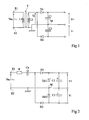
- FIG. 1 shows a first example of a converter AC / DC (AC / DC) classic with positive outputs and negative.
- This converter uses a transformer T whose the primary winding L1 receives on two terminals E1 and E2 a alternating voltage Vac (for example, the 240 V / 50 Hz mains or 110 V / 60 Hz).
- the two terminals of the secondary L2 of the transformer T deliver an AC low voltage whose amplitude peak corresponds approximately to the desired values for the converter output V + and V- voltages.
- Each tension V +, V- is taken from the terminals of a capacitor, respectively C1, C2.
- Each capacitor is connected in series with a diode, respectively D1, D2, on the secondary winding L2 of the transformer.
- the anode of diode D1 and the cathode diode D2 are connected to the upper terminal of the winding L2.
- the common point M of capacitors C1 and C2, which constitutes the reference of the voltages V + and V-, is connected to the terminal input E2.
- Figure 2 shows a second classic example of AC-DC converter capable of delivering two voltages of output V + and V- of opposite signs.
- a high voltage capacitor Cx is connected via a resistor R of low value at input terminal E1.
- the second terminal of the capacitor Cx is connected via diodes rectification D1, D2 to low voltage capacitors C1 and C2 the second terminals of which are connected to a reference terminal M connected to terminal E2.
- a Zener diode, DZ1, DZ2, is in parallel on each of the capacitors C1, C2.
- the capacitor Cx has a low value compared to that of each of the capacitors C1, C2 so as to oppose a high impedance to the variations of the input voltage.
- the converters described above are relatively simple to use due to the small number of components used. However, these converters have the disadvantage essential their size and cost.
- the present invention provides a new solution to make a converter of a high alternating voltage in two symmetrical continuous low voltages, which overcomes the disadvantages of known solutions.
- the invention aims, in particular, to propose a new solution whose size is minimized.
- the invention also relates to a solution which respects electromagnetic compatibility constraints.
- the present invention also provides a new converter which automatically adapts to current requirements of the load. More particularly, the present invention offers a solution adapted to a wide range of currents, that is to say which allows, if necessary, to deliver currents significantly more important than conventional solutions without cause significant losses.
- the present invention further aims to improve the regulating the output voltage of the converter.
- the present invention provides a converter receiving an alternating voltage between a input terminal and a reference terminal and providing two direct voltages of opposite polarities across the terminals of a first and a second capacitor, a common terminal of which is connected to the reference terminal.
- This converter includes a first unidirectional switch connected between the input terminal and a node of the circuit; a third capacitor, connected, in parallel with the first capacitor, between said node and the reference point; a circuit means comprising a second switch to connect the second capacitor in series with the third capacitor when the second switch is closed ; and a control circuit to close the first switch only at the beginning and at the end of alternating polarity given, the second switch being open when the first switch is closed.
- the circuit means comprises a controllable current source to ensure the passage of a constant current.
- the second switch is connected between said node and the reference point.
- the first capacitor is connected to said node via a first diode, the third capacitor being connected, via a third diode to the terminal of reference.
- a second diode is connected between the second capacitor and the connection point of the third capacitor and the third diode.
- control circuit receives information on the voltage continues across the first capacitor and controls the first switch so that this DC voltage is substantially constant.
- the first switch is controllable in voltage or current on opening and closing and is able to block tension of the sector live or in reverse when it is not ordered to the passing state.
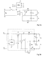
- a converter according to the present invention receives on two terminals input 11 and 12 an alternating voltage, terminal 12 constituting a reference terminal.
- the DC output voltages V + and V- are available to capacitor terminals C1 and C2 which have a common terminal M constituting the converter reference terminal, connected to the terminal 12.
- a one-way switch K is connected by sound anode to a terminal 11 and by its cathode to a terminal 13. Between the terminals 13 and 12 are arranged in parallel the capacitor C1 in series with a diode D1, and a capacitor C3 in series with a diode D3. Diodes D1 and D3 are polarized to be conductive when terminal 13 is positive with respect to terminal 12. The anode of diode D1 is connected to terminal 13. The cathode of diode D3 is connected to terminal 12. A diode D2 is connected by its anode at the terminal of capacitor C2 not connected to point M and by its cathode at the connection point of capacitor C3 and diode D3. A switch K 'is connected between the terminals 13 and 12.
- CTRL control circuit 15
- the control circuit 15 also receives (in the purpose of regulating the value of the output voltage) information on the voltage present across the capacitor C1.
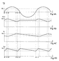
- FIGS. 4A to 4D represent, in the form of chronograms, an example of pace characteristic voltages of the converter according to the invention.
- FIG. 4A represents the alternating voltage Vac.
- Figure 4B represents the voltage VC3 across the capacitor C3.
- the Figure 4C represents the output voltage V- across the capacitor C2.
- Figure 4D shows the output voltage V + across capacitor C1. For the sake of simplification and unless otherwise specified, no account is taken of falls from voltage in the circuit diodes.
- the circuit 15 controls the switch K so that it is closed only at the start and at the end of each positive alternation of the voltage Vac, for periods t 0 -t 1 at the start of alternation and t 2 -t 3 at the end of alternation.
- the switch K ' is open during these periods.
- the circuit 15 causes the opening of the switch K as a result of the detection of the fact that the voltage V + has reached the desired value V0.
- the capacitor C1 begins to discharge while supplying the voltage V + to a load.
- the power supply energy for the loads is then supplied by the capacitors C1 and C2.
- the supply voltage across the capacitor C3 remains constant between t 1 and t 4 and between t 5 and t 2, however .
- the circuit 15 causes the switch K 'to close. This results in a discharge of the capacitor C3 in the capacitor C2 via the path C3, K ', C2, D2.
- the voltages across the capacitors C2 and C3 balance each other.
- a circuit (not shown in FIG. 3A) suitable for ensuring a discharge at constant current.
- the delay in closing the switch K 'relative to the opening of the switch K (instants t 1 to t 4 ) is intended to avoid any risk of simultaneous conduction of these switches, which would have the effect short-circuit the AC power supply.
- the switch K ′ is open, in the vicinity of the end of the alternation, at an instant t 5 prior to the instant t 2 of closing of the switch K.
- the capacitors C1 and C2 supply the loads (not shown) which are connected to them, the switch K being open and the switch K 'being optionally open or closed.
- the converter of the invention adapts well to a variation in the energy required by one of the loads.
- FIG. 3B shows the same circuit as Figure 3A.
- the elements have been arranged so that all the components being part of the same silicon chip are arranged to inside a frame 21.
- the only non-integrated elements are then the capacitors C1, C2 and C3.
- Switch K has been represented as a T component such as a bipolar transistor with an isolated gate (IGBT) associated with a gate switch k.
- component T is a switch leaving pass current in one direction, voltage controllable or running at opening and closing, suitable for block the mains voltage in reverse, and live when it is not in the passing state.
- the switch K has been shown in the form of a current source controlled to be blocked or active.
- An advantage of the present invention is that no current is not taken from alternative food outside of neighborhood of the zero crossing of an alternation.
- the invention minimizes therefore the power dissipated from the circuit by limiting the periods of energy drawn from the network near zero alternations and avoids the generation of current pulses important when opening and closing switch K.
- Another advantage of the invention is that it does not require the use of high power passive components voltage.
- Another advantage of the invention is that the tensions V + and V- are regulated with respect to neutral 12 of the alternating voltage Vac.
Landscapes
- Engineering & Computer Science (AREA)
- Power Engineering (AREA)
- Rectifiers (AREA)
Applications Claiming Priority (2)
| Application Number | Priority Date | Filing Date | Title |
|---|---|---|---|
| FR9910088 | 1999-07-30 | ||
| FR9910088A FR2797115B1 (fr) | 1999-07-30 | 1999-07-30 | Convertisseur alternatif-continu non-isole |
Publications (1)
| Publication Number | Publication Date |
|---|---|
| EP1073190A1 true EP1073190A1 (de) | 2001-01-31 |
Family
ID=9548851
Family Applications (1)
| Application Number | Title | Priority Date | Filing Date |
|---|---|---|---|
| EP00410087A Withdrawn EP1073190A1 (de) | 1999-07-30 | 2000-07-28 | Nichtisolierter Wechselstrom-Gleichstromwandler |
Country Status (3)
| Country | Link |
|---|---|
| US (1) | US6400588B1 (de) |
| EP (1) | EP1073190A1 (de) |
| FR (1) | FR2797115B1 (de) |
Families Citing this family (4)
| Publication number | Priority date | Publication date | Assignee | Title |
|---|---|---|---|---|
| ITTO20010219A1 (it) * | 2001-03-09 | 2002-09-09 | St Microelectronics Srl | Convertitore ac/dc e dc/dc a bassa potenza e uscita duale. |
| JP3841049B2 (ja) * | 2002-12-27 | 2006-11-01 | ヤマハ株式会社 | 電源回路 |
| US20190097524A1 (en) * | 2011-09-13 | 2019-03-28 | Fsp Technology Inc. | Circuit having snubber circuit in power supply device |
| US9584011B1 (en) * | 2016-01-06 | 2017-02-28 | Semiconductor Components Industries, Llc | Capacitive coupled input transfer gates |
Citations (7)
| Publication number | Priority date | Publication date | Assignee | Title |
|---|---|---|---|---|
| US3938025A (en) * | 1973-10-17 | 1976-02-10 | Telefonaktiebolaget L M Ericsson | DC to DC converter for producing two individually controlled and stabilized DC-voltages |
| DE3341767A1 (de) * | 1983-11-18 | 1985-05-30 | Siemens AG, 1000 Berlin und 8000 München | Spannungsschaltregler |
| EP0292148A2 (de) * | 1987-05-15 | 1988-11-23 | Linear Technology Corporation | Kapazitive Spannungswandlerschaltung mit niedriger Sättigungsspannung und Strombegrenzungsschalter |
| JPH05219738A (ja) * | 1992-02-07 | 1993-08-27 | Matsushita Electric Ind Co Ltd | 多重出力スイッチングレギュレータ |
| EP0601593A2 (de) * | 1992-12-11 | 1994-06-15 | Moulinex S.A. | Stromvervielfacher-Versorgungsvorrichtung |
| US5606491A (en) * | 1995-06-05 | 1997-02-25 | Analog Devices, Inc. | Multiplying and inverting charge pump |
| US5896284A (en) * | 1995-08-11 | 1999-04-20 | Nippon Steel Corporation | Switching power supply apparatus with a return circuit that provides a return energy to a load |
Family Cites Families (7)
| Publication number | Priority date | Publication date | Assignee | Title |
|---|---|---|---|---|
| US4807104A (en) * | 1988-04-15 | 1989-02-21 | Motorola, Inc. | Voltage multiplying and inverting charge pump |
| US5051882A (en) * | 1989-01-27 | 1991-09-24 | Teledyne Industries | Three reservoir capacitor charge pump circuit |
| JPH04222455A (ja) * | 1990-12-20 | 1992-08-12 | Nec Corp | インタフェース回路 |
| JPH05268763A (ja) * | 1992-03-17 | 1993-10-15 | Nec Corp | Dc/dcコンバータ回路およびそれを用いたrs−232インタフェース回路 |
| US5306954A (en) * | 1992-06-04 | 1994-04-26 | Sipex Corporation | Charge pump with symmetrical +V and -V outputs |
| US5262934A (en) * | 1992-06-23 | 1993-11-16 | Analogic Corporation | Bipolar voltage doubler circuit |
| JPH0828965B2 (ja) * | 1992-09-02 | 1996-03-21 | 日本電気株式会社 | 電圧変換回路 |
-
1999
- 1999-07-30 FR FR9910088A patent/FR2797115B1/fr not_active Expired - Fee Related
-
2000
- 2000-07-28 EP EP00410087A patent/EP1073190A1/de not_active Withdrawn
- 2000-07-28 US US09/628,052 patent/US6400588B1/en not_active Expired - Lifetime
Patent Citations (7)
| Publication number | Priority date | Publication date | Assignee | Title |
|---|---|---|---|---|
| US3938025A (en) * | 1973-10-17 | 1976-02-10 | Telefonaktiebolaget L M Ericsson | DC to DC converter for producing two individually controlled and stabilized DC-voltages |
| DE3341767A1 (de) * | 1983-11-18 | 1985-05-30 | Siemens AG, 1000 Berlin und 8000 München | Spannungsschaltregler |
| EP0292148A2 (de) * | 1987-05-15 | 1988-11-23 | Linear Technology Corporation | Kapazitive Spannungswandlerschaltung mit niedriger Sättigungsspannung und Strombegrenzungsschalter |
| JPH05219738A (ja) * | 1992-02-07 | 1993-08-27 | Matsushita Electric Ind Co Ltd | 多重出力スイッチングレギュレータ |
| EP0601593A2 (de) * | 1992-12-11 | 1994-06-15 | Moulinex S.A. | Stromvervielfacher-Versorgungsvorrichtung |
| US5606491A (en) * | 1995-06-05 | 1997-02-25 | Analog Devices, Inc. | Multiplying and inverting charge pump |
| US5896284A (en) * | 1995-08-11 | 1999-04-20 | Nippon Steel Corporation | Switching power supply apparatus with a return circuit that provides a return energy to a load |
Non-Patent Citations (1)
| Title |
|---|
| PATENT ABSTRACTS OF JAPAN vol. 17, no. 668 (E - 1473) 9 December 1993 (1993-12-09) * |
Also Published As
| Publication number | Publication date |
|---|---|
| US6400588B1 (en) | 2002-06-04 |
| FR2797115A1 (fr) | 2001-02-02 |
| FR2797115B1 (fr) | 2001-10-12 |
Similar Documents
| Publication | Publication Date | Title |
|---|---|---|
| EP3422554B1 (de) | Reversibler ac/dc-wandler mit thyristoren | |
| EP1626493A1 (de) | Kapazitives Netzteil | |
| FR3037741A1 (fr) | Convertisseur a circuit correcteur du facteur de puissance | |
| EP0820141B1 (de) | Nullspannungsansteuerung einer hybriden Brückenschaltung | |
| FR3068546A1 (fr) | Convertisseur ac/dc reversible a triacs | |
| EP3010133A1 (de) | Anordnung zur kontrollierten gleichrichtung | |
| FR2547106A1 (fr) | Dispositif d'equilibrage d'interrupteurs connectes en serie | |
| FR2977996A1 (fr) | Convertisseur de puissance comportant un module onduleur a transistors a effet de champ normalement fermes | |
| EP0798838B1 (de) | Schaltung zur Verbesserung des Leistungsfaktors mit doppelter Entladung | |
| FR2742010A1 (fr) | Dispositif d'amelioration du facteur de puissance d'une alimentation redressee | |
| EP1073190A1 (de) | Nichtisolierter Wechselstrom-Gleichstromwandler | |
| FR2876515A1 (fr) | Circuit d'alimentation double | |
| FR2859580A1 (fr) | Gradateur pour charges resistives ou capacitives | |
| FR2969417A1 (fr) | Alimentation capacitive a limitation de courant d'appel | |
| EP0843412B1 (de) | Anwesenheitsdetektor mit einer stabilisierten Stromquelle | |
| EP4115512A1 (de) | Verfahren und vorrichtung zur umwandlung einer spannung mit weichem schalten der schalter | |
| FR2778286A1 (fr) | Circuit convertisseur de tension | |
| EP1014551A1 (de) | Hochwechselspannung-Niedergleichspannungswandler | |
| FR2498038A1 (fr) | Montage electrique pour le fonctionnement a plusieurs allures de resistances chauffantes et d'un moteur de ventilateur, par exemple dans un seche-cheveux | |
| EP0032089B1 (de) | Speiseschaltung für eine elektrische Last, insbesondere für eine Entladungslampe | |
| FR2974255A1 (fr) | Circuit d'alimentation capacitive | |
| EP1434340B1 (de) | Isolierte Niederspannungsversorgung | |
| FR2969870A1 (fr) | Circuit de commande d'un interrupteur en serie avec un element capacitif | |
| EP0821469A1 (de) | Hoch- und Niederspannungsgleichstromversorgung | |
| EP1005145A1 (de) | Hoch- und Niederspannungsgleichstromversorgung |
Legal Events
| Date | Code | Title | Description |
|---|---|---|---|
| PUAI | Public reference made under article 153(3) epc to a published international application that has entered the european phase |
Free format text: ORIGINAL CODE: 0009012 |
|
| AK | Designated contracting states |
Kind code of ref document: A1 Designated state(s): DE FR GB IT |
|
| AX | Request for extension of the european patent |
Free format text: AL;LT;LV;MK;RO;SI |
|
| 17P | Request for examination filed |
Effective date: 20010716 |
|
| AKX | Designation fees paid |
Free format text: DE FR GB IT |
|
| RAP1 | Party data changed (applicant data changed or rights of an application transferred) |
Owner name: STMICROELECTRONICS S.A. |
|
| 17Q | First examination report despatched |
Effective date: 20080605 |
|
| STAA | Information on the status of an ep patent application or granted ep patent |
Free format text: STATUS: THE APPLICATION IS DEEMED TO BE WITHDRAWN |
|
| 18D | Application deemed to be withdrawn |
Effective date: 20081016 |