EP1073198A2 - Résonateur à couche mince et procédé de fabrication - Google Patents
Résonateur à couche mince et procédé de fabrication Download PDFInfo
- Publication number
- EP1073198A2 EP1073198A2 EP00306072A EP00306072A EP1073198A2 EP 1073198 A2 EP1073198 A2 EP 1073198A2 EP 00306072 A EP00306072 A EP 00306072A EP 00306072 A EP00306072 A EP 00306072A EP 1073198 A2 EP1073198 A2 EP 1073198A2
- Authority
- EP
- European Patent Office
- Prior art keywords
- substrate
- piezoelectric film
- film
- electrode
- piezoelectric
- Prior art date
- Legal status (The legal status is an assumption and is not a legal conclusion. Google has not performed a legal analysis and makes no representation as to the accuracy of the status listed.)
- Granted
Links
Images
Classifications
-
- H—ELECTRICITY
- H10—SEMICONDUCTOR DEVICES; ELECTRIC SOLID-STATE DEVICES NOT OTHERWISE PROVIDED FOR
- H10N—ELECTRIC SOLID-STATE DEVICES NOT OTHERWISE PROVIDED FOR
- H10N30/00—Piezoelectric or electrostrictive devices
-
- H—ELECTRICITY
- H03—ELECTRONIC CIRCUITRY
- H03H—IMPEDANCE NETWORKS, e.g. RESONANT CIRCUITS; RESONATORS
- H03H9/00—Networks comprising electromechanical or electro-acoustic elements; Electromechanical resonators
- H03H9/15—Constructional features of resonators consisting of piezoelectric or electrostrictive material
- H03H9/17—Constructional features of resonators consisting of piezoelectric or electrostrictive material having a single resonator
- H03H9/171—Constructional features of resonators consisting of piezoelectric or electrostrictive material having a single resonator implemented with thin-film techniques, i.e. of the film bulk acoustic resonator [FBAR] type
- H03H9/172—Means for mounting on a substrate, i.e. means constituting the material interface confining the waves to a volume
- H03H9/174—Membranes
-
- H—ELECTRICITY
- H03—ELECTRONIC CIRCUITRY
- H03H—IMPEDANCE NETWORKS, e.g. RESONANT CIRCUITS; RESONATORS
- H03H3/00—Apparatus or processes specially adapted for the manufacture of impedance networks, resonating circuits, resonators
- H03H3/007—Apparatus or processes specially adapted for the manufacture of impedance networks, resonating circuits, resonators for the manufacture of electromechanical resonators or networks
- H03H3/02—Apparatus or processes specially adapted for the manufacture of impedance networks, resonating circuits, resonators for the manufacture of electromechanical resonators or networks for the manufacture of piezoelectric or electrostrictive resonators or networks
-
- H—ELECTRICITY
- H03—ELECTRONIC CIRCUITRY
- H03H—IMPEDANCE NETWORKS, e.g. RESONANT CIRCUITS; RESONATORS
- H03H9/00—Networks comprising electromechanical or electro-acoustic elements; Electromechanical resonators
- H03H9/15—Constructional features of resonators consisting of piezoelectric or electrostrictive material
-
- H—ELECTRICITY
- H03—ELECTRONIC CIRCUITRY
- H03H—IMPEDANCE NETWORKS, e.g. RESONANT CIRCUITS; RESONATORS
- H03H3/00—Apparatus or processes specially adapted for the manufacture of impedance networks, resonating circuits, resonators
- H03H3/007—Apparatus or processes specially adapted for the manufacture of impedance networks, resonating circuits, resonators for the manufacture of electromechanical resonators or networks
- H03H3/02—Apparatus or processes specially adapted for the manufacture of impedance networks, resonating circuits, resonators for the manufacture of electromechanical resonators or networks for the manufacture of piezoelectric or electrostrictive resonators or networks
- H03H2003/023—Apparatus or processes specially adapted for the manufacture of impedance networks, resonating circuits, resonators for the manufacture of electromechanical resonators or networks for the manufacture of piezoelectric or electrostrictive resonators or networks the resonators or networks being of the membrane type
-
- Y—GENERAL TAGGING OF NEW TECHNOLOGICAL DEVELOPMENTS; GENERAL TAGGING OF CROSS-SECTIONAL TECHNOLOGIES SPANNING OVER SEVERAL SECTIONS OF THE IPC; TECHNICAL SUBJECTS COVERED BY FORMER USPC CROSS-REFERENCE ART COLLECTIONS [XRACs] AND DIGESTS
- Y10—TECHNICAL SUBJECTS COVERED BY FORMER USPC
- Y10T—TECHNICAL SUBJECTS COVERED BY FORMER US CLASSIFICATION
- Y10T29/00—Metal working
- Y10T29/42—Piezoelectric device making
Definitions
- This invention relates to thin film resonators (TFRs) and a method of making TFRs.
- TFRs are thin film acoustic devices which can resonate in the radio frequency to microwave range, for example, .5 to 5 Gigahertz (GHz), in response to an electrical signal.
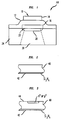
- FIG. 1 shows a typical TFR 10 with a piezoelectric film 12 between a first electrode 14 and a second electrode 16 which apply an electric field to the piezoelectric film 12.
- the film 12 is made of a piezoelectric crystalline material, such as zinc oxide, aluminum nitrite (AlN) and other piezoelectric crystalline material, which exhibits a piezoelectric effect.
- the piezoelectric effect occurs when the peiezoelectric material expands or contracts in response to an electric field applied across the piezoelectric material, for example by the first and second electrodes 14 and 16, or produces an electric field in response to mechanical stress or strain applied to the piezoelectric material.
- the film 12 will mechanically vibrate at the resonant frequencies which in turn produces an alternating electric field at the resonant frequencies.
- the first and second electrodes 14 and 16 are typically of metal, such as aluminum.
- the acoustic impedance mismatch between the first electrode 14 and the air creates a first acoustic reflecting surface 18 at the interface between the top surface of the first electrode 14 and the air.
- a second acoustic reflecting surface 22 can be established at an interface between the second electrode 16 and a substrate 24 (or air if a portion of the substrate 24 under the film 12 is removed).
- acoustic reflecting layer(s) can be created between the second electrode 16 and the substrate 24 to suppress unwanted frequencies, such as harmonics of the fundamental frequency.
- the acoustic reflecting layer(s) can be formed from a material having desired characteristic acoustic impedance(s) and with the proper dimensions to provide desired reflection characteristics for the second reflecting surface at the interface between the second electrode 14 and the acoustic reflecting layers. As such, the acoustic reflecting layers can reflect desired frequencies while suppressing unwanted frequencies.
- An acoustic cavity created between the first and second reflecting surfaces and with the proper dimensions establishes a standing wave at the resonant frequencies of the piezoelectric film 12.
- the dimensions of the acoustic cavity for example the thickness of the piezoelectric film 12 and the electrodes 14 and 16, define the operating frequencies for the TFR 10. Energy outside the operating frequencies of the TFR 10 is lost, while energy within the operating frequencies is preserved.
- the TFR 10 structure can be formed on the substrate 24, such as a silicon (Si), Gallium Arsenide (GaAs) or other semiconductor substrate, for monolithic integration purposes, such as integration with active semiconductor devices.
- the TFR 10 is typically formed on other suitable substrates, such as quartz, sapphire, aluminum nitride (AlN), or silicon carbide. If the TFR 10 has acoustic reflecting layer(s), the acoustic reflecting layer(s) are formed on the substrate 24 followed by the second electrode 16 which is formed on the reflecting layer(s). If there are no acoustic reflecting layers, then the second electrode 16 is formed on the substrate 24, for example using chemical vapor deposition (CVD) or sputtering.
- CVD chemical vapor deposition
- the piezoelectric film 12 is then formed on the second electrode 16, and the first electrode 14 is formed on top of the piezoelectric film 12, for example using chemical vapor deposition (CVD) or sputtering.
- CVD chemical vapor deposition
- a portion of the substrate 24 is removed from under the second reflecting surface 22.
- the substrate 24 includes an etch stop 28, such as a boron doped p+ layer implanted in a silicon (Si) substrate, at the upper surface of the substrate 24 adjacent to the bottom of the second electrode 16.
- the etch stop 28 is used to protect the second electrode 16 from a chemical etch removing the portion 30 of the substrate 24.
- the resulting piezoelectric film 12 is polycrystalline in that distinct crystals having different lattice orientations are present throughout the piezoelectric film 12. Such a non-uniform or irregular crystalline structure with grain boundaries between the differently oriented crystallites or crystal grains reduces the quality of the piezoelectric film 12.
- the quality factor Q for a TFR is a measure of the resonance quality of the acoustic cavity while the coupling coefficient is a measure of the efficiency of conversion between electrical and mechanical energy within the acoustic cavity. Both of these figures of merit are inversely proportional to the acoustic loss introduced by the TFR at the operating frequency band.
- the piezoelectric film 10 has a polycrystalline structure with grain boundaries and other defects, such as point imperfections or dislocations in the crystal lattice, or poor reflectivity of the reflecting surfaces 18 and 22 for example due to surface roughness, acoustic losses can result from acoustic scattering within the film 12 and acoustic radiation into the surrounding areas of the device 10. Thus, if the film 12 is polycrystalline, acoustic losses will be introduced by the film 12, thereby producing a lower quality TFR.
- TFRs can be used at radio frequency (RF) because piezoelectric films can be made thin, for example at higher frequencies, such as .5-10 GHz, the piezoelectric film 12 can be between .4 and 8 microns in width. Because TFRs produce an alternating electric field at the resonant frequency in response to an alternating electric field having frequency components corresponding to the resonant frequencies, TFRs can be used as radio frequency (RF) filter elements. TFR filters have a distinct size advantage over conventional RF filters, such as those based on ceramics. For example, thin film resonators can have volumes of 1.5 cubic millimeters while ceramic resonators are typically notless than hundreds of cubic millimeters in volume.
- a ceramic element typically introduces more loss to the input signal at the operating frequency band than the TFR.
- TFR also have higher power handling capabilities than surface acoustic wave (SAW) devices, for example 200 milliwatts vs. 2 watts.
- SAW surface acoustic wave
- TFRs can introduce losses to an electrical signal applied to the TFR in part due to the polycrystalline structure of the film 12.
- Typical TFR fabricating methods produce piezoelectric films with on the order of 10 8 distinct crystalline orientations separated by grain boundaries.
- the present invention involves a thin film resonator (TFR) produced with an improved piezoelectric film which is epitaxially grown on a growing surface, resulting in a piezoelectric film with less grain boundaries.
- Epitaxial growth refers to the piezoelectric film having a crystallographic orientation taken from or emulating the crystallographic orientation of a single crystal substrate or growing surface.
- a method of making a TFR is disclosed in which the piezoelectric film is grown on a substrate. Subsequently, a portion of the substrate is removed, and the electrodes are deposited on either side of the piezoelectric film.
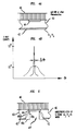
- a single crystal silicon (Si) substrate 40 is provided on which a piezoelectric film is epitaxially formed for the acoustic cavity of the TFR.
- Epitaxial growth in the context of this invention refers to the formation of a crystalline film with a crystallographic orientation taken from or emulating a single crystal substrate or an imposed template pattern on a growing surface.
- the piezoelectric film is epitaxially formed to have a uniform, regular or continuous crystallographic orientation based on the uniform, regular or continuous crystollographic orientation of the substrate, for example a single crystal silicon substrate.
- Non-epitaxial growth of the piezoelectric film typically leads to grain boundaries which contribute to acoustic energy losses within the resulting TFR and result in device degradation through aging and fatigue at the grain boundaries. The epitaxial growth results in fewer grain boundaries and improved structural integrity.
- any deviation in a crystal from a perfect periodic lattice is an imperfection.
- a point imperfection is localized at a point in the lattice structure and can occur due to chemical impurities, vacant lattice sites and interstitial atoms (extra atoms not in the regular lattice).
- a line of imperfections, such as a dislocation is a discontinuity in the crystal lattice structure.
- the crystal orientation typically, on either side of the dislocation, the crystal orientation has the same regular periodic arrangement. Arrays of dislocations can form grain boundaries between adjoining crystallites or crystal grains which have distinct crystallographic orientations. Non-epitaxial growth typically leads to grain boundaries which produce an irregular and discontinuous crystalline orientation within the film.
- Non-epitaxial growth of piezoelectric film for TFRs typically can have 10 8 grain boundaries per cm 2 and 10 10 dislocations per cm 2 .
- the non-epitaxial piezoetectric film is thereby polycrystalline with a discontinuous and irregular crystalline structure, and the dislocations are typically dispersed throughout the piezoelectric film.
- a high quality epitaxial piezoelectric film grown on an approximately lattice-matched single crystal substrate typically has very few (for example less than 10 distinct crystallographic orientations within the film) or no grain boundaries with 10 5 -10 10 dislocations per cm 2 at the substrate-heteroepitaxial interface.
- the number of dislocations decreases by a factor of two every 2-3000 angstroms, and the dislocations are typically parallel to or along the direction of growth.
- Epitaxial growth of a piezoelectric film on a substrate can be obtained when the substrate and the piezoelectric film has a crystalline structure with similar in-plane lattice parameters.
- a film can be epitaxially grown on a substrate when the in-plane lattice mismatch between the piezoelectric film and the underlying material (the substrate upon which the piezoelectric film is being deposited) is less than 20%.
- Lattice mismatch is equal to [(a0/a0(substrate))-1] where a0 and a0(substrate) are respectively the in-plane lattice parameters of the deposited thin film and the material upon which the thin film is deposited.
- the crystal orientation of the substrate can be varied to reduce the lattice mismatch between the parallel lattice planes of the substrate 40 and the film to be deposited on the substrate 40.
- a Si substrate 40 with a ⁇ 111 ⁇ orientation can be obtained for epitaxially growing a AlN film.
- a substrate 40 with a ⁇ 110 ⁇ or ⁇ 100 ⁇ orientation can also be sufficient.
- Other substrates can include gallium arsenide, galium nitride and others.
- the piezoelectric film can be epitaxially formed on the substrate 40 with a reduced number of grain boundaries.
- Single crystal Si substrates have zero grain boundaries and zero dislocations while a single crystal GaAs substrate has zero grain boundaries and 10-10 5 dislocations per cm 2 .
- Epitaxial deposition of a variety of materials is discussed in Mathews, Epitaxial Growth , Academic Press, 1975.
- other substrates or growing surfaces for example gallium arsenide, gallium nitride, or aluminum oxide, can be used having different, amorphous or even irregular and discontinuous crystalline orientations so long as the piezoelectric film is epitaxially formed with the desired continuous, uniform or regular crystalline orientation.
- epitaxial growth can occur using grapho-epitaxy, where a growing surface is prepared with physical growth sites or structures, such as grooves, pits, etchings or a pattern to epitaxially form a film having a particular continuous, uniform or regular crystalline orientation.
- a film can be epitaxially formed over an amorphously structured material, such as an oxide (for example aluminum oxide), through lateral epitaxial growth which starts with the epitaxial formation of the film on an appropriate growing surface adjacent to the amorphous structure, and the film forms epitaxially with respect to the growing surface over the amorphous structure.
- an amorphously structured material such as an oxide (for example aluminum oxide)
- a piezoelectric film for the acoustic cavity of the film can include a first piezoelectric film epitaxially grown with respect to a first growing surface or substrate adjacent to a second piezoelectric film having a different crystalline orientation and epitaxially grown with respect to a second growing surface or substrate.
- a first piezoelectric film epitaxially grown on a first growing surface can be adjacent to a non-epitaxially grown film on a second growing surface.
- the first and second piezoelectric films are different, and/or the growing surfaces or substrates are different.
- the single crystal Si substrate 40 can be formed from commercially available single crystal Si wafers which are about .5 -1 millimeter thick.
- a mask 42 is deposited on the substrate 40, such as a mask of silicon nitride Si 3 N 4 .
- Other masks could be used which are resistant to the etch subsequently used on the substrate 40.
- the mask 42 can be deposited for example using low pressure chemical vapor deposition (LPCVD) or other deposition techniques. See, Kern & Vossen, "Thin Film Processes," Vols. I and II, Wiley & Sons.
- an etch stop 44 is produced on the substrate 40 for use in resisting the subsequent anistropic or isotropic etching of the substrate 40.
- the type of etch stop can vary.
- the etch stop 44 can be produced by epitaxial growth or ion implantation, for example to produce a phosphorus or boron-doped n + or p + etch stop 44 having a dopant level of greater than 10 20 atoms per cubic centimeter. Other etch stops or dopant concentrations are possible.
- a piezoelectric crystalline film 46 such as aluminum nitride (AlN) is epitaxially grown on the substrate 40.
- the piezoelectric film 46 can be epitaxially grown on the substrate 40 using molecular beam epitaxy (MBE).
- MBE molecular beam epitaxy
- Si (111) is used as the substrate on which the AlN film is epitaxially formed with the c axis of the film along the direction of growth.
- the Si (111) substrate is cleaned in buffered oxide etch (BOE), spun dry in air, and loaded into the MBE vacuum. In the MBE vacuum, the substrate is heated to 950 degrees celsius to desorb the residual oxide from the substrate.
- BOE buffered oxide etch
- the clean Si (111) substrate is lowered to 800 degrees celsius, whereby the Si (111) 7 X 7 silicon surface reconstruction shows a reflecting high energy electron diffraction (RHEED) pattern which indicates a clean (111) surface ready for epitaxial growth.
- the AlN film is nucleated at a substrate temperature of 600 - 800 degrees celsius to a thickness of 100 angstroms using a growth rate of 775 angstroms per hour.
- the substrate is then raised to a temperature of 920 degrees celsius for 200 angstroms more growth of AlN at 775 angstroms per hour.
- the substrate is further raised to 980-1020 degrees celsius to complete the growing of the AlN film again at 775 angstroms per hour.
- the film 46 can be produced with less contamination, resulting in fewer defects.
- the defects produce scattering of the acoustic energy which results in acoustic losses.
- Other methods can be used to epitaxially produce the film 46 on the substrate 40, such as sputtering and metallo organic chemical vapor deposition (CVD). See, Kern & Vossen, "Thin Film Processes," Vols. I and II, Wiley & Sons.
- the piezoelectric film 46 is epitaxially formed on the substrate 40 which has a continuous crystalline orientation
- the piezoelectric film 46 is produced having a continuous crystalline orientation, such as a single crystal AlN film 46, with relatively few or no grain boundaries along the substrate.
- the epitaxial film 46 may have dislocations or other imperfections, but these defects can also be reduced if the substrate is epitaxially formed on the substrate 40 which has suitable lattice mismatch and a continuous crystalline orientation.
- the piezoelectric film 46 can be scanned using x-ray diffraction microscopy to determine if the piezoelectric film is uniformly oriented and has a low defect density.
- the sharpness or width of the diffraction peak can measure whether the film is highly oriented, for example a diffraction peak less than 1 degree thick throughout the film, indicates a film having a continuous crystalline orientation.
- FIG. 4b shows an example of an x-ray diffraction peak for an epitaxial piezoelectric film with a ⁇ of .5 degree and an intensity of 10 6 counts.
- the dashed line shows an example x-ray diffraction peak for a non-epitaxial piezoelectric film with a x-ray diffraction peak about 3 degrees wide and an intensity of 10 4 counts.
- the intensity of the peak can provide an indication of the defect density.
- typical non-epitaxial film has an intensity on the order of 10 4 counts.
- a transmission electron microscope (TEM) or defect etching can be used to determine the defect density of the film.
- defects In using a TEM, a portion of the crystalline material is sliced off and thinned down to a thickness through which electrons can pass. Because the defects have a different transmission coefficient than the surrounding material, defects can be detected by electron counts. Defect etching involves using a chemical etch to enhance the film defects which have a different etching rate than the surrounding material. Then, the defects are simply counted.
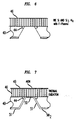
- a portion 47 of the silicon substrate 40 is removed from under the film 46 using an anisotropic or isotropic etch after removing a portion of the silicon nitride mask 42.
- different etchants can be used.
- an anisotropic etch can be performed using ehylene damine procatechol (EDP).
- EDP ehylene damine procatechol
- An anisotropic etch can also be performed using potassium hydroxide (KOH) at 80 degrees celsius to achieve the same etching rate.
- an isotropic etch can be performed for example using plasma etching if using a chromium (Cr) mask.
- the silicon etches typically attack most metals, including aluminum and aluminum nitride. Consequently, in this embodiment, the etch stop 44 protects the AlN film 46 from the etch.
- Dashed lines 48 show the effects of different types of etches on the substrate 40.
- Dashed line 48a illustrates the effects of an anisotropic etch using for example EDP or KOH
- dashed line 48b shows the effects of an isotropic etch
- dashed line 48c shows the effects of other anistropic etches, for example using reactive ion etching (RIE), to achieve a different etching profile.
- RIE reactive ion etching
- the etch stop 44 acts by not being substantially etched under the conditions used to etch the underlying layer.
- the etch stop 44 and the remaining mask 42 can be removed by reactive ion etching (RIE) with Fluorine chemistry which attacks the silicon but stops at the AlN film 46 in this embodiment.
- RIE reactive ion etching
- Fluorine chemistry which attacks the silicon but stops at the AlN film 46 in this embodiment.
- the etch stop 44 is not removed.
- other etching techniques can be used.
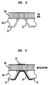
- the film 46 and the remaining substrate 40 are oxidized, for example using thermal oxidation or anodization, as shown in FIG. 7.
- the silicon oxide layer is added to provide electrical isolation of the electrodes from the silicon substrate.
- Non-conducting substrates, such as GaAs and aluminum oxide, would not require isolation form the electrodes.
- the piezoelectric film 46 for example of AlN, has a low oxidation rate when compared to the substrate 40, for example of silicon, thin layers 49 and 50 of aluminum oxinitrite (AlON), for example 100-200 angstroms thick, are produced on the AlN film 46.
- AlON aluminum oxinitrite
- the silicon substrate is oxidized to form a layer 51 of silicon dioxide (SiO 2 ), for example of 1000-2000 angstroms thick.
- the AlON layers 49 and 50 on the top and bottom of the film 46 are removed using chlorine based chemistry which has little effect on the layer 51 of silicon dioxide as shown in FIG. 8.
- the layers 49 and 50 can be selectively etched to remove the layer 49 and/or the layer 50, or both layers 49 and 50 can be retained.
- electrodes 52 and 54 are produced on either side of the film 46 to form a capacitor with the film 46.
- the electrodes 52 and 54 are deposited by sputtering which is typically performed using Argon gas as a sputtering gas, for example using a M2000 sputtering system from Novellus of Santa Clara California, USA.
- Argon gas as a sputtering gas
- M2000 sputtering system from Novellus of Santa Clara California, USA.
- this type of sputtering involves placing an electric field and Argon between the TFR being fabricated and an aluminum (Al) target.
- the Argon ions are attracted to the Al target and bombard the Al target, releasing Al ions and neutral species which are deposited on the top and/or bottom (as well as the substrate 40) of the film 46.
- Other electrode deposition techniques can be used, such as chemical vapor deposition (CVD).
- an improved thin film resonator is produced with less grain boundaries to reduce losses introduced by the TFR to electrical signals at certain frequencies corresponding to the resonant frequencies of the TFR, for example .1 to 10 GHz.
- the film can be formed with different thicknesses.
- alternative embodiments of the method of fabricating the TFR are possible which omit and/or add steps and/or use variations or portions of the described method.
- alternative embodiments of the resulting TFR are possible which add and/or omit layers and/or structures and/or use variations or portions of the described TFR.
- the layer 48 and/or 49 can be removed and/or retained before the electrodes 52 and 54 are deposited.
- additional layers of for example reflecting layers can be included in the manufacturing of the TFR or subsequently added to the TFR.
- the TFR is described as being fabricated with particular materials and using particular etches, but alternative materials and etches can be used to fabricate the TFR according to the principles of the present invention.
- other piezoelectric crystalline films such as zinc oxide, as well as other piezoelectric materials can be used.
- the TFR is described with the piezoelectric film being grown on a single crystal Si substrate but other growing surfaces are possible which epitaxially produce a uniform crystalline structure in the film based on the crystallographic orientation of the substrate or on the growing surface.
- the film 12 can be epitaxially grown using grapho-epitaxy in which case the electrode surface can be the growing surface which has been patterned or textured, for example with a periodic, regular pattern.
- the periodic regular patterned surface can be formed to emulate a surface of a single crystal substrate.
- a regular periodic pattern of mezas and/or grooves can be used as seeds for the piezoelectric film using spacing commensurate with the spacing of the lattice structure of the piezoelectric film, such as the same spacing or a multiple of the spacing between the parallel lattice planes.
- the pattern can be formed using lithographic and/or etching techniques. Growing processes could be similar to those described above or would be understood by one of skill in the art with the benefit of this disclosure.
- LEGO a substrate or appropriate growing surface is adjacent to the electrode over which the piezoelectric film is grown as would be understood by one of skill in the art with the benefit of this disclosure.
- a single crystal electrode with the appropriate lattice structure could be used as an electrode on which the piezoelectric film is grown.
- the various materials making up the TFR and their respective physical characteristics can determine the order and manner of certain manufacturing steps and processes.
- the electrode can be deposited before the film.
Landscapes
- Physics & Mathematics (AREA)
- Acoustics & Sound (AREA)
- Engineering & Computer Science (AREA)
- Manufacturing & Machinery (AREA)
- Piezo-Electric Or Mechanical Vibrators, Or Delay Or Filter Circuits (AREA)
- Crystals, And After-Treatments Of Crystals (AREA)
- Physical Vapour Deposition (AREA)
- Chemical Vapour Deposition (AREA)
Applications Claiming Priority (2)
| Application Number | Priority Date | Filing Date | Title |
|---|---|---|---|
| US09/363,527 US6349454B1 (en) | 1999-07-29 | 1999-07-29 | Method of making thin film resonator apparatus |
| US363527 | 1999-07-29 |
Publications (3)
| Publication Number | Publication Date |
|---|---|
| EP1073198A2 true EP1073198A2 (fr) | 2001-01-31 |
| EP1073198A3 EP1073198A3 (fr) | 2001-02-07 |
| EP1073198B1 EP1073198B1 (fr) | 2007-11-07 |
Family
ID=23430596
Family Applications (1)
| Application Number | Title | Priority Date | Filing Date |
|---|---|---|---|
| EP00306072A Expired - Lifetime EP1073198B1 (fr) | 1999-07-29 | 2000-07-17 | Résonateur à couche mince et procédé de fabrication |
Country Status (9)
| Country | Link |
|---|---|
| US (1) | US6349454B1 (fr) |
| EP (1) | EP1073198B1 (fr) |
| JP (1) | JP2001094373A (fr) |
| KR (1) | KR100438467B1 (fr) |
| CN (1) | CN1283895A (fr) |
| AU (1) | AU4884000A (fr) |
| BR (1) | BR0002976A (fr) |
| CA (1) | CA2314375C (fr) |
| DE (1) | DE60036988T2 (fr) |
Cited By (4)
| Publication number | Priority date | Publication date | Assignee | Title |
|---|---|---|---|---|
| WO2003017481A1 (fr) * | 2001-08-14 | 2003-02-27 | Koninklijke Philips Electronics N.V. | Ensemble filtre comportant un resonateur a ondes de volume |
| EP1306973A2 (fr) | 2001-10-26 | 2003-05-02 | Fujitsu Limited | Résonateur piézoélectrique à couche mince, filtre passe bande et procédé de fabrication d'un résonateur piézoélectrique à couche mince |
| WO2003052929A1 (fr) | 2001-12-17 | 2003-06-26 | Intel Corporation | Structure et procedures de fabrication permettant de produire des resonateurs acoustiques a substrat pelliculaire ayant un facteur q eleve et un faible affaiblissement d'insertion |
| WO2004030208A2 (fr) | 2002-09-25 | 2004-04-08 | Intel Corporation | Fabrication de resonateurs acoustiques a ondes de volume pelliculaires sur des plaquettes de silicium, faisant appel a une attaque anisotropique dependant d'une orientation cristalline |
Families Citing this family (55)
| Publication number | Priority date | Publication date | Assignee | Title |
|---|---|---|---|---|
| US6593193B2 (en) * | 2001-02-27 | 2003-07-15 | Matsushita Electric Industrial Co., Ltd. | Semiconductor device and method for fabricating the same |
| US6816035B2 (en) * | 2002-08-08 | 2004-11-09 | Intel Corporation | Forming film bulk acoustic resonator filters |
| US20040027030A1 (en) * | 2002-08-08 | 2004-02-12 | Li-Peng Wang | Manufacturing film bulk acoustic resonator filters |
| GB2406582A (en) * | 2002-08-13 | 2005-04-06 | Trikon Technologies Ltd | Acoustic resonators |
| US6741147B2 (en) * | 2002-09-30 | 2004-05-25 | Agere Systems Inc. | Method and apparatus for adjusting the resonant frequency of a thin film resonator |
| KR100483340B1 (ko) * | 2002-10-22 | 2005-04-15 | 쌍신전자통신주식회사 | 체적탄성파 소자 및 그 제조방법 |
| JP3966237B2 (ja) * | 2003-06-19 | 2007-08-29 | セイコーエプソン株式会社 | 圧電デバイス、圧電デバイスを搭載した電子機器 |
| US6904666B2 (en) * | 2003-07-31 | 2005-06-14 | Andrew Corporation | Method of manufacturing microwave filter components and microwave filter components formed thereby |
| US7230367B2 (en) * | 2003-11-07 | 2007-06-12 | Matsushita Electric Industrial Co., Ltd. | Piezoelectric resonator, production method thereof, filter, duplexer, and communication device |
| US7242130B2 (en) * | 2003-11-07 | 2007-07-10 | Matsushita Electric Industrial Co., Ltd. | Piezoelectric device, antenna duplexer, and method of manufacturing piezoelectric resonators used therefor |
| US7113055B2 (en) * | 2003-11-07 | 2006-09-26 | Matsushita Electric Industrial Co., Ltd. | Piezoelectric resonator, method of manufacturing piezoelectric resonator, and filter, duplexer, and communication device using piezoelectric resonator |
| US7323805B2 (en) | 2004-01-28 | 2008-01-29 | Kabushiki Kaisha Toshiba | Piezoelectric thin film device and method for manufacturing the same |
| KR100622955B1 (ko) * | 2004-04-06 | 2006-09-18 | 삼성전자주식회사 | 박막 벌크 음향 공진기 및 그 제조방법 |
| JP4077805B2 (ja) * | 2004-04-23 | 2008-04-23 | 松下電器産業株式会社 | 共振器の製造方法 |
| JP4149416B2 (ja) * | 2004-05-31 | 2008-09-10 | 富士通メディアデバイス株式会社 | 圧電薄膜共振子およびフィルタならびにそれらの製造方法 |
| JPWO2006062082A1 (ja) * | 2004-12-07 | 2008-06-12 | 松下電器産業株式会社 | 薄膜弾性波共振子 |
| US20060274476A1 (en) * | 2005-04-13 | 2006-12-07 | Andrew Cervin-Lawry | Low loss thin film capacitor and methods of manufacturing the same |
| WO2006112260A1 (fr) * | 2005-04-13 | 2006-10-26 | Murata Manufacturing Co., Ltd. | Filtre a film mince piezo-electrique |
| US20070063777A1 (en) * | 2005-08-26 | 2007-03-22 | Mircea Capanu | Electrostrictive devices |
| US7319284B2 (en) * | 2005-09-02 | 2008-01-15 | Precision Instrument Development Center National Applied Research Laboratories | Surface acoustic wave device and method for fabricating the same |
| KR100780842B1 (ko) * | 2006-12-14 | 2007-11-30 | 주식회사 에스세라 | 공진 구조체를 가지는 압전 공진자의 형성방법들 |
| US9369105B1 (en) * | 2007-08-31 | 2016-06-14 | Rf Micro Devices, Inc. | Method for manufacturing a vibrating MEMS circuit |
| US9391588B2 (en) | 2007-08-31 | 2016-07-12 | Rf Micro Devices, Inc. | MEMS vibrating structure using an orientation dependent single-crystal piezoelectric thin film layer |
| US9385685B2 (en) | 2007-08-31 | 2016-07-05 | Rf Micro Devices, Inc. | MEMS vibrating structure using an orientation dependent single-crystal piezoelectric thin film layer |
| US8231795B2 (en) * | 2009-05-01 | 2012-07-31 | Avago Technologies Wireless Ip (Singapore) Pte. Ltd. | Micromachined horn |
| US9117593B2 (en) | 2012-11-02 | 2015-08-25 | Rf Micro Devices, Inc. | Tunable and switchable resonator and filter structures in single crystal piezoelectric MEMS devices using bimorphs |
| CA3197453C (fr) | 2013-03-16 | 2025-07-08 | Leslie Don Roberts | Cartouche d’analyse modulaire et autonome et système programmable de distribution de réactif |
| CN103281050A (zh) * | 2013-06-17 | 2013-09-04 | 天津大学 | 薄膜体声波滤波器 |
| US9355972B2 (en) * | 2014-03-04 | 2016-05-31 | International Business Machines Corporation | Method for making a dielectric region in a bulk silicon substrate providing a high-Q passive resonator |
| US9991872B2 (en) | 2014-04-04 | 2018-06-05 | Qorvo Us, Inc. | MEMS resonator with functional layers |
| US9998088B2 (en) | 2014-05-02 | 2018-06-12 | Qorvo Us, Inc. | Enhanced MEMS vibrating device |
| US9571061B2 (en) * | 2014-06-06 | 2017-02-14 | Akoustis, Inc. | Integrated circuit configured with two or more single crystal acoustic resonator devices |
| US9537465B1 (en) * | 2014-06-06 | 2017-01-03 | Akoustis, Inc. | Acoustic resonator device with single crystal piezo material and capacitor on a bulk substrate |
| KR101598294B1 (ko) * | 2014-09-15 | 2016-02-26 | 삼성전기주식회사 | 음향 공진기 및 그 제조 방법 |
| KR102117471B1 (ko) * | 2015-01-12 | 2020-06-01 | 삼성전기주식회사 | 음향 공진기 및 그 제조 방법 |
| US11476825B2 (en) * | 2016-03-11 | 2022-10-18 | Akoustis, Inc. | 5.5 GHz Wi-Fi coexistence acoustic wave resonator RF filter circuit |
| US10979026B2 (en) * | 2016-03-11 | 2021-04-13 | Akoustis, Inc. | 5.5 GHz Wi-fi 5G coexistence acoustic wave resonator RF filter circuit |
| US10979025B2 (en) * | 2016-03-11 | 2021-04-13 | Akoustis, Inc. | 5G band n79 acoustic wave resonator RF filter circuit |
| US10979022B2 (en) * | 2016-03-11 | 2021-04-13 | Akoustis, Inc. | 5.2 GHz Wi-Fi acoustic wave resonator RF filter circuit |
| US11451213B2 (en) * | 2016-03-11 | 2022-09-20 | Akoustis, Inc. | 5G n79 Wi-Fi acoustic triplexer circuit |
| US11418169B2 (en) * | 2016-03-11 | 2022-08-16 | Akoustis, Inc. | 5G n41 2.6 GHz band acoustic wave resonator RF filter circuit |
| US10979024B2 (en) * | 2016-03-11 | 2021-04-13 | Akoustis, Inc. | 5.2 GHz Wi-Fi coexistence acoustic wave resonator RF filter circuit |
| US11316496B2 (en) * | 2016-03-11 | 2022-04-26 | Akoustis, Inc. | Method and structure for high performance resonance circuit with single crystal piezoelectric capacitor dielectric material |
| US10985732B2 (en) * | 2016-03-11 | 2021-04-20 | Akoustis, Inc. | 5.6 GHz Wi-Fi acoustic wave resonator RF filter circuit |
| US10979023B2 (en) * | 2016-03-11 | 2021-04-13 | Akoustis, Inc. | 5.9 GHz c-V2X and DSRC acoustic wave resonator RF filter circuit |
| CN107342357B (zh) * | 2016-04-28 | 2022-08-16 | 新科实业有限公司 | 薄膜压电元件及其制造方法 |
| US10432172B2 (en) * | 2016-09-01 | 2019-10-01 | Samsung Electro-Mechanics Co., Ltd. | Bulk acoustic filter device and method of manufacturing the same |
| US11171628B2 (en) * | 2017-07-04 | 2021-11-09 | Samsung Electro-Mechanics Co., Ltd. | Acoustic resonator and method for manufacturing the same |
| JP7298991B2 (ja) * | 2018-01-22 | 2023-06-27 | 太陽誘電株式会社 | 圧電薄膜共振器、フィルタおよびマルチプレクサ |
| CN108900173B (zh) * | 2018-07-04 | 2022-03-04 | 杭州左蓝微电子技术有限公司 | 一种以硅为牺牲层的薄膜体声波谐振器制备方法 |
| CN110957989B (zh) * | 2018-09-26 | 2024-01-26 | 中国科学院苏州纳米技术与纳米仿生研究所 | 薄膜体声波谐振器及其制作方法 |
| CN113541630B (zh) * | 2020-04-21 | 2026-03-03 | 济南晶正电子科技有限公司 | 一种复合单晶压电基板及其制备方法 |
| CN111988010B (zh) * | 2020-08-24 | 2025-06-27 | 苏州奥谱毫通电子科技有限公司 | 一种晶体滤波元件 |
| CN113300683B (zh) * | 2021-05-25 | 2023-03-10 | 中国科学院上海微系统与信息技术研究所 | 一种声表面波谐振器及其制备方法 |
| US12362724B2 (en) * | 2021-08-20 | 2025-07-15 | Raytheon Company | N-polar rare-earth III-nitride bulk acoustic wave resonator |
Family Cites Families (17)
| Publication number | Priority date | Publication date | Assignee | Title |
|---|---|---|---|---|
| US3422371A (en) | 1967-07-24 | 1969-01-14 | Sanders Associates Inc | Thin film piezoelectric oscillator |
| US4320365A (en) | 1980-11-03 | 1982-03-16 | United Technologies Corporation | Fundamental, longitudinal, thickness mode bulk wave resonator |
| JPS5859618A (ja) * | 1981-10-05 | 1983-04-08 | Nobuo Mikoshiba | 弾性表面波素子 |
| JPS59141812A (ja) * | 1983-02-02 | 1984-08-14 | Nec Corp | 薄膜圧電振動子 |
| JPS60145715A (ja) * | 1984-01-09 | 1985-08-01 | Nippon Telegr & Teleph Corp <Ntt> | 圧電共振子形成用基板の製造方法 |
| JPS60210018A (ja) * | 1984-04-03 | 1985-10-22 | Nec Corp | 薄膜圧電振動子 |
| US4719383A (en) * | 1985-05-20 | 1988-01-12 | The United States Of America As Represented By The United States Department Of Energy | Piezoelectric shear wave resonator and method of making same |
| JPH07101832B2 (ja) * | 1986-06-23 | 1995-11-01 | 株式会社日立製作所 | 圧電変換器及びその製造方法 |
| JPS6369280A (ja) * | 1986-09-10 | 1988-03-29 | Hitachi Ltd | 圧電素子及びその製造方法 |
| JPH02248110A (ja) * | 1989-03-20 | 1990-10-03 | Sanyo Electric Co Ltd | 弾性表面波素子 |
| US5747857A (en) * | 1991-03-13 | 1998-05-05 | Matsushita Electric Industrial Co., Ltd. | Electronic components having high-frequency elements and methods of manufacture therefor |
| JPH07122960A (ja) * | 1993-10-22 | 1995-05-12 | Sanyo Electric Co Ltd | 弾性表面波素子 |
| JPH07142954A (ja) * | 1993-11-15 | 1995-06-02 | Murata Mfg Co Ltd | 圧電薄膜複合共振子およびその製造方法 |
| US5864261A (en) | 1994-05-23 | 1999-01-26 | Iowa State University Research Foundation | Multiple layer acoustical structures for thin-film resonator based circuits and systems |
| US5821833A (en) | 1995-12-26 | 1998-10-13 | Tfr Technologies, Inc. | Stacked crystal filter device and method of making |
| FR2746229B1 (fr) * | 1996-03-15 | 1998-05-22 | Dispositif electronique comprenant une base de temps integree | |
| JPH09321361A (ja) * | 1996-05-27 | 1997-12-12 | Tdk Corp | 圧電振動部品及びその製造方法 |
-
1999
- 1999-07-29 US US09/363,527 patent/US6349454B1/en not_active Expired - Lifetime
-
2000
- 2000-07-17 DE DE60036988T patent/DE60036988T2/de not_active Expired - Lifetime
- 2000-07-17 EP EP00306072A patent/EP1073198B1/fr not_active Expired - Lifetime
- 2000-07-19 BR BR0002976-9A patent/BR0002976A/pt not_active Application Discontinuation
- 2000-07-24 CA CA002314375A patent/CA2314375C/fr not_active Expired - Fee Related
- 2000-07-26 AU AU48840/00A patent/AU4884000A/en not_active Abandoned
- 2000-07-26 CN CN00121944A patent/CN1283895A/zh active Pending
- 2000-07-27 JP JP2000226698A patent/JP2001094373A/ja active Pending
- 2000-07-28 KR KR10-2000-0043698A patent/KR100438467B1/ko not_active Expired - Lifetime
Cited By (12)
| Publication number | Priority date | Publication date | Assignee | Title |
|---|---|---|---|---|
| WO2003017481A1 (fr) * | 2001-08-14 | 2003-02-27 | Koninklijke Philips Electronics N.V. | Ensemble filtre comportant un resonateur a ondes de volume |
| US6975182B2 (en) * | 2001-08-14 | 2005-12-13 | Koninklijke Philips Electronics N.V. | Filter system with bulk wave resonator having a reflection layer composition that varies with the layer thickness |
| CN1541447B (zh) * | 2001-08-14 | 2010-04-21 | Nxp股份有限公司 | 带有体波谐振器的滤波系统 |
| EP1306973A2 (fr) | 2001-10-26 | 2003-05-02 | Fujitsu Limited | Résonateur piézoélectrique à couche mince, filtre passe bande et procédé de fabrication d'un résonateur piézoélectrique à couche mince |
| WO2003052929A1 (fr) | 2001-12-17 | 2003-06-26 | Intel Corporation | Structure et procedures de fabrication permettant de produire des resonateurs acoustiques a substrat pelliculaire ayant un facteur q eleve et un faible affaiblissement d'insertion |
| US6662419B2 (en) | 2001-12-17 | 2003-12-16 | Intel Corporation | Method for fabricating film bulk acoustic resonators to achieve high-Q and low loss |
| US6861783B2 (en) | 2001-12-17 | 2005-03-01 | Intel Corporation | Structure to achieve high-Q and low insertion loss film bulk acoustic resonators |
| US7116034B2 (en) | 2001-12-17 | 2006-10-03 | Intel Corporation | Structure to achieve high-Q and low insertion loss film bulk acoustic resonators |
| CN1620755B (zh) * | 2001-12-17 | 2011-06-22 | 英特尔公司 | 形成基片中的器件的方法和薄膜体声共振器 |
| WO2004030208A2 (fr) | 2002-09-25 | 2004-04-08 | Intel Corporation | Fabrication de resonateurs acoustiques a ondes de volume pelliculaires sur des plaquettes de silicium, faisant appel a une attaque anisotropique dependant d'une orientation cristalline |
| WO2004030208A3 (fr) * | 2002-09-25 | 2004-07-22 | Intel Corp | Fabrication de resonateurs acoustiques a ondes de volume pelliculaires sur des plaquettes de silicium, faisant appel a une attaque anisotropique dependant d'une orientation cristalline |
| US7152289B2 (en) | 2002-09-25 | 2006-12-26 | Intel Corporation | Method for forming bulk resonators silicon <110> substrate |
Also Published As
| Publication number | Publication date |
|---|---|
| BR0002976A (pt) | 2001-03-13 |
| CA2314375A1 (fr) | 2001-01-29 |
| AU4884000A (en) | 2001-02-01 |
| US6349454B1 (en) | 2002-02-26 |
| DE60036988T2 (de) | 2008-08-28 |
| CN1283895A (zh) | 2001-02-14 |
| EP1073198A3 (fr) | 2001-02-07 |
| EP1073198B1 (fr) | 2007-11-07 |
| JP2001094373A (ja) | 2001-04-06 |
| KR100438467B1 (ko) | 2004-07-03 |
| KR20010030029A (ko) | 2001-04-16 |
| DE60036988D1 (de) | 2007-12-20 |
| CA2314375C (fr) | 2003-11-18 |
Similar Documents
| Publication | Publication Date | Title |
|---|---|---|
| US6349454B1 (en) | Method of making thin film resonator apparatus | |
| US11909380B2 (en) | Acoustic resonator and method of manufacturing the same | |
| US7057470B2 (en) | Quartz oscillator and method for manufacturing the same | |
| US4640756A (en) | Method of making a piezoelectric shear wave resonator | |
| Park et al. | A 10 GHz single-crystalline scandium-doped aluminum nitride Lamb-wave resonator | |
| US8436516B2 (en) | Resonator device including electrode with buried temperature compensating layer | |
| Zhao et al. | 15-ghz epitaxial aln fbars on sic substrates | |
| US10587241B2 (en) | Temperature compensated acoustic resonator device having thin seed interlayer | |
| US20130049545A1 (en) | Resonator device including electrodes with buried temperature compensating layers | |
| CN113285014A (zh) | 单晶掺杂薄膜、声波谐振器用压电薄膜及其制备方法 | |
| TW202145607A (zh) | 體聲波共振器以及製造體聲波共振器之方法 | |
| JP4373936B2 (ja) | 薄膜圧電共振器及びその製造方法 | |
| WO2019228750A1 (fr) | Procédé de fabrication d'un résonateur à ondes acoustiques de volume et dispositif de résonateur à ondes acoustiques de volume | |
| CN116346067A (zh) | 空腔型体声波谐振器及其制作方法 | |
| KR100609508B1 (ko) | 에어갭 타입 에프비에이알장치 및 그 제조방법 | |
| CN115580253B (zh) | 一种单晶压电薄膜体声波谐振器的制备方法 | |
| US20210207286A1 (en) | Mechanical Oscillator and Method for Producing Same | |
| US20250330146A1 (en) | N-polar rare-earth iii-nitride bulk acoustic wave resonator | |
| CN121664135A (zh) | 空腔型体声波谐振器的制作方法 | |
| KR20030057520A (ko) | 보조 씨드를 이용한 압전층 우선배향 및 fbar밴드패스필터제작. |
Legal Events
| Date | Code | Title | Description |
|---|---|---|---|
| PUAI | Public reference made under article 153(3) epc to a published international application that has entered the european phase |
Free format text: ORIGINAL CODE: 0009012 |
|
| PUAL | Search report despatched |
Free format text: ORIGINAL CODE: 0009013 |
|
| AK | Designated contracting states |
Kind code of ref document: A2 Designated state(s): DE FR GB |
|
| AX | Request for extension of the european patent |
Free format text: AL;LT;LV;MK;RO;SI |
|
| AK | Designated contracting states |
Kind code of ref document: A3 Designated state(s): AT BE CH CY DE DK ES FI FR GB GR IE IT LI LU MC NL PT SE |
|
| AX | Request for extension of the european patent |
Free format text: AL;LT;LV;MK;RO;SI |
|
| 17P | Request for examination filed |
Effective date: 20010522 |
|
| AKX | Designation fees paid |
Free format text: DE FR GB |
|
| 17Q | First examination report despatched |
Effective date: 20061002 |
|
| GRAP | Despatch of communication of intention to grant a patent |
Free format text: ORIGINAL CODE: EPIDOSNIGR1 |
|
| GRAS | Grant fee paid |
Free format text: ORIGINAL CODE: EPIDOSNIGR3 |
|
| GRAA | (expected) grant |
Free format text: ORIGINAL CODE: 0009210 |
|
| AK | Designated contracting states |
Kind code of ref document: B1 Designated state(s): DE FR GB |
|
| REG | Reference to a national code |
Ref country code: GB Ref legal event code: FG4D |
|
| REF | Corresponds to: |
Ref document number: 60036988 Country of ref document: DE Date of ref document: 20071220 Kind code of ref document: P |
|
| ET | Fr: translation filed | ||
| PLBE | No opposition filed within time limit |
Free format text: ORIGINAL CODE: 0009261 |
|
| STAA | Information on the status of an ep patent application or granted ep patent |
Free format text: STATUS: NO OPPOSITION FILED WITHIN TIME LIMIT |
|
| 26N | No opposition filed |
Effective date: 20080808 |
|
| PGFP | Annual fee paid to national office [announced via postgrant information from national office to epo] |
Ref country code: FR Payment date: 20130724 Year of fee payment: 14 |
|
| PGFP | Annual fee paid to national office [announced via postgrant information from national office to epo] |
Ref country code: GB Payment date: 20140716 Year of fee payment: 15 |
|
| REG | Reference to a national code |
Ref country code: DE Ref legal event code: R082 Ref document number: 60036988 Country of ref document: DE Representative=s name: DILG HAEUSLER SCHINDELMANN PATENTANWALTSGESELL, DE |
|
| REG | Reference to a national code |
Ref country code: FR Ref legal event code: ST Effective date: 20150331 |
|
| PG25 | Lapsed in a contracting state [announced via postgrant information from national office to epo] |
Ref country code: FR Free format text: LAPSE BECAUSE OF NON-PAYMENT OF DUE FEES Effective date: 20140731 |
|
| GBPC | Gb: european patent ceased through non-payment of renewal fee |
Effective date: 20150717 |
|
| PG25 | Lapsed in a contracting state [announced via postgrant information from national office to epo] |
Ref country code: GB Free format text: LAPSE BECAUSE OF NON-PAYMENT OF DUE FEES Effective date: 20150717 |
|
| REG | Reference to a national code |
Ref country code: DE Ref legal event code: R082 Ref document number: 60036988 Country of ref document: DE Representative=s name: DILG, HAEUSLER, SCHINDELMANN PATENTANWALTSGESE, DE Ref country code: DE Ref legal event code: R082 Ref document number: 60036988 Country of ref document: DE Representative=s name: DILG HAEUSLER SCHINDELMANN PATENTANWALTSGESELL, DE Ref country code: DE Ref legal event code: R081 Ref document number: 60036988 Country of ref document: DE Owner name: AVAGO TECHNOLOGIES GENERAL IP (SINGAPORE) PTE., SG Free format text: FORMER OWNER: LUCENT TECHNOLOGIES INC., MURRAY HILL, N.J., US Ref country code: DE Ref legal event code: R081 Ref document number: 60036988 Country of ref document: DE Owner name: AVAGO TECHNOLOGIES INTERNATIONAL SALES PTE. LI, SG Free format text: FORMER OWNER: LUCENT TECHNOLOGIES INC., MURRAY HILL, N.J., US |
|
| REG | Reference to a national code |
Ref country code: DE Ref legal event code: R081 Ref document number: 60036988 Country of ref document: DE Owner name: AVAGO TECHNOLOGIES INTERNATIONAL SALES PTE. LI, SG Free format text: FORMER OWNER: AVAGO TECHNOLOGIES GENERAL IP (SINGAPORE) PTE. LTD., SINGAPORE, SG Ref country code: DE Ref legal event code: R082 Ref document number: 60036988 Country of ref document: DE Representative=s name: DILG, HAEUSLER, SCHINDELMANN PATENTANWALTSGESE, DE Ref country code: DE Ref legal event code: R082 Ref document number: 60036988 Country of ref document: DE Representative=s name: DILG HAEUSLER SCHINDELMANN PATENTANWALTSGESELL, DE |
|
| PGFP | Annual fee paid to national office [announced via postgrant information from national office to epo] |
Ref country code: DE Payment date: 20190729 Year of fee payment: 20 |
|
| REG | Reference to a national code |
Ref country code: DE Ref legal event code: R071 Ref document number: 60036988 Country of ref document: DE |