EP1076403A2 - Leistungswandler mit mehreren Betriebsarten und Ausgleichsschaltungen und zugehöriges Betriebsverfahren - Google Patents
Leistungswandler mit mehreren Betriebsarten und Ausgleichsschaltungen und zugehöriges Betriebsverfahren Download PDFInfo
- Publication number
- EP1076403A2 EP1076403A2 EP00115097A EP00115097A EP1076403A2 EP 1076403 A2 EP1076403 A2 EP 1076403A2 EP 00115097 A EP00115097 A EP 00115097A EP 00115097 A EP00115097 A EP 00115097A EP 1076403 A2 EP1076403 A2 EP 1076403A2
- Authority
- EP
- European Patent Office
- Prior art keywords
- voltage
- switches
- bus
- switch
- approximately
- Prior art date
- Legal status (The legal status is an assumption and is not a legal conclusion. Google has not performed a legal analysis and makes no representation as to the accuracy of the status listed.)
- Withdrawn
Links
Images






Classifications
-
- H—ELECTRICITY
- H02—GENERATION; CONVERSION OR DISTRIBUTION OF ELECTRIC POWER
- H02J—ELECTRIC POWER NETWORKS; CIRCUIT ARRANGEMENTS OR SYSTEMS FOR SUPPLYING OR DISTRIBUTING ELECTRIC POWER; SYSTEMS FOR STORING ELECTRIC ENERGY
- H02J9/00—Circuit arrangements for emergency or stand-by power supply, e.g. for emergency lighting
- H02J9/04—Circuit arrangements for emergency or stand-by power supply, e.g. for emergency lighting in which the distribution system is disconnected from the normal source and connected to a standby source
- H02J9/06—Circuit arrangements for emergency or stand-by power supply, e.g. for emergency lighting in which the distribution system is disconnected from the normal source and connected to a standby source with automatic change-over, e.g. UPS systems
- H02J9/062—Circuit arrangements for emergency or stand-by power supply, e.g. for emergency lighting in which the distribution system is disconnected from the normal source and connected to a standby source with automatic change-over, e.g. UPS systems for AC powered loads
-
- H—ELECTRICITY
- H02—GENERATION; CONVERSION OR DISTRIBUTION OF ELECTRIC POWER
- H02J—ELECTRIC POWER NETWORKS; CIRCUIT ARRANGEMENTS OR SYSTEMS FOR SUPPLYING OR DISTRIBUTING ELECTRIC POWER; SYSTEMS FOR STORING ELECTRIC ENERGY
- H02J9/00—Circuit arrangements for emergency or stand-by power supply, e.g. for emergency lighting
- H02J9/04—Circuit arrangements for emergency or stand-by power supply, e.g. for emergency lighting in which the distribution system is disconnected from the normal source and connected to a standby source
- H02J9/06—Circuit arrangements for emergency or stand-by power supply, e.g. for emergency lighting in which the distribution system is disconnected from the normal source and connected to a standby source with automatic change-over, e.g. UPS systems
- H02J9/061—Circuit arrangements for emergency or stand-by power supply, e.g. for emergency lighting in which the distribution system is disconnected from the normal source and connected to a standby source with automatic change-over, e.g. UPS systems for DC powered loads
-
- H—ELECTRICITY
- H02—GENERATION; CONVERSION OR DISTRIBUTION OF ELECTRIC POWER
- H02M—APPARATUS FOR CONVERSION BETWEEN AC AND AC, BETWEEN AC AND DC, OR BETWEEN DC AND DC, AND FOR USE WITH MAINS OR SIMILAR POWER SUPPLY SYSTEMS; CONVERSION OF DC OR AC INPUT POWER INTO SURGE OUTPUT POWER; CONTROL OR REGULATION THEREOF
- H02M5/00—Conversion of AC power input into AC power output, e.g. for change of voltage, for change of frequency, for change of number of phases
- H02M5/40—Conversion of AC power input into AC power output, e.g. for change of voltage, for change of frequency, for change of number of phases with intermediate conversion into DC
- H02M5/42—Conversion of AC power input into AC power output, e.g. for change of voltage, for change of frequency, for change of number of phases with intermediate conversion into DC by static converters
- H02M5/44—Conversion of AC power input into AC power output, e.g. for change of voltage, for change of frequency, for change of number of phases with intermediate conversion into DC by static converters using discharge tubes or semiconductor devices to convert the intermediate DC into AC
- H02M5/453—Conversion of AC power input into AC power output, e.g. for change of voltage, for change of frequency, for change of number of phases with intermediate conversion into DC by static converters using discharge tubes or semiconductor devices to convert the intermediate DC into AC using devices of a triode or transistor type requiring continuous application of a control signal
- H02M5/458—Conversion of AC power input into AC power output, e.g. for change of voltage, for change of frequency, for change of number of phases with intermediate conversion into DC by static converters using discharge tubes or semiconductor devices to convert the intermediate DC into AC using devices of a triode or transistor type requiring continuous application of a control signal using semiconductor devices only
- H02M5/4585—Conversion of AC power input into AC power output, e.g. for change of voltage, for change of frequency, for change of number of phases with intermediate conversion into DC by static converters using discharge tubes or semiconductor devices to convert the intermediate DC into AC using devices of a triode or transistor type requiring continuous application of a control signal using semiconductor devices only having a rectifier with controlled elements
-
- H—ELECTRICITY
- H02—GENERATION; CONVERSION OR DISTRIBUTION OF ELECTRIC POWER
- H02J—ELECTRIC POWER NETWORKS; CIRCUIT ARRANGEMENTS OR SYSTEMS FOR SUPPLYING OR DISTRIBUTING ELECTRIC POWER; SYSTEMS FOR STORING ELECTRIC ENERGY
- H02J9/00—Circuit arrangements for emergency or stand-by power supply, e.g. for emergency lighting
- H02J9/04—Circuit arrangements for emergency or stand-by power supply, e.g. for emergency lighting in which the distribution system is disconnected from the normal source and connected to a standby source
- H02J9/06—Circuit arrangements for emergency or stand-by power supply, e.g. for emergency lighting in which the distribution system is disconnected from the normal source and connected to a standby source with automatic change-over, e.g. UPS systems
- H02J9/062—Circuit arrangements for emergency or stand-by power supply, e.g. for emergency lighting in which the distribution system is disconnected from the normal source and connected to a standby source with automatic change-over, e.g. UPS systems for AC powered loads
- H02J9/063—Common neutral, e.g. AC input neutral line connected to AC output neutral line and DC middle point
Definitions
- the present invention relates to electrical power devices and methods of operation thereof, and more particularly, to power conversion devices and methods of operation thereof.
- UPSs Uninterruptible power supplies
- UPSs are power conversion devices that are commonly used to provide conditioned, reliable power for computer networks, telecommunications networks, medical equipment and the like. UPSs are widely used with computers and similar computing devices, including but not limited to personal computers, workstations, mini computers, network servers, disk arrays and mainframe computers, to insure that valuable data is not lost and that the device can continue to operate notwithstanding temporary loss of an AC utility source. UPSs typically provide power to such electronic equipment from a secondary source, such as a battery, in the event that a primary alternating current (AC) utility source drops out (blackout) or fails to provide a proper voltage (brownout).
- AC primary alternating current
- a typical off-line UPS disconnects a load from a primary AC source 10 when the primary AC source fails or is operating in a degraded manner, allowing the load to be served from a secondary source such as a battery.
- the AC power source 10 is connected in series with a switch S 1 , producing an AC voltage across a load 20 when the switch S 1 is closed.
- Energy storage is typically provided in the form of a storage capacitor C S .
- the secondary power source here a battery B
- the switch S 1 is opened, causing the load to draw power from the battery B .
- the low voltage converter 30 typically is an inverter that produces a quasi-square wave or sine wave voltage on a first winding L 1 of the transformer T from a DC voltage produced by the battery B .
- the first winding L 1 is coupled to a second winding L 2 of the transformer T connected across the load 20 .
- the battery B may be charged using the low-voltage converter 30 or a separate battery charger circuit (not shown).
- FIG. 2 A line interactive (LIA) UPS topology is illustrated in Fig. 2.
- the transformer T has a third winding L 3 that may be connected in series with the load 20 using switches S 2 , S 3 to "buck" or "boost” the voltage applied to the load 20 .
- the switch S 1 can be opened to allow the load 20 to run off the battery B .
- a typical on-line UPS includes a rectifier 40 that receives an AC voltage from an AC power source 10 , producing a DC voltage across a storage capacitor C S at an intermediate node 45 .
- An inverter 50 is connected between the intermediate node 45 , and is operative to produce an AC voltage across a load 20 from the DC voltage.
- a battery B is connected to the intermediate node 45 via a DC/DC converter 60 , supplying auxiliary power.
- the DC/DC converter can be eliminated and a high-voltage battery (not shown) connected directly to the intermediate node 45 .
- Each of these topologies may have disadvantages.
- typical conventional on-line and LIA UPSs for 60 Hz applications use 60 Hz magnetic components (e.g., transformers and inductors) that are sized for such frequencies, and thus may be large, heavy and expensive.
- LIA UPSs often exhibit step voltage changes that can affect the performance of the load.
- Conventional off-line, LIA and on-line UPSs often use large storage capacitors, which tend to be bulky and expensive, in order to maintain an acceptable output voltage under heavy loading conditions.
- sellers of UPSs may be required to maintain large inventories including several different types of UPSs in order to meet a variety of different customer applications.
- a rectifier circuit produces first and second voltages (e.g., ⁇ DC voltages) on first and second voltage busses from an AC input voltage produced by an AC power source
- an inverter circuit produces an AC output voltage from the first and second voltages
- a balancer circuit controls the relative magnitudes of the first and second voltages responsive to respective first and second rates at which the balancer circuit couples the first and second voltage busses to a neutral bus of the AC power source.
- the rectifier circuit includes first and second switches that selectively couple the first and second voltage busses to a phase bus of the AC power source through a first inductance
- the inverter circuit includes third and fourth switches that selectively couple the first and second voltage busses to a load through a second inductance
- the balancer circuit includes fifth and sixth switches that selectively couple the first and second voltage bussed to the neutral bus through a third inductance, such as an inductor or transformer winding.
- the balancer circuit enables energy transfer between first and second storage capacitors connected between the neutral bus and the first and second voltage busses, respectively, thus allowing the storage capacitors to be smaller than the storage capacitors typically used in conventional power converters with comparable power ratings.
- the switches in the rectifier, inductor and balancer can be controlled such that the power converter can be operated in a number of different power transfer modes.
- a secondary power source such as a battery, may also be coupled to the power converter via a winding of a transformer that also serves as an inductance for the balancer circuit. In one embodiment, this coupling may be achieved through a combination battery converter/battery charger circuit that can also charge the battery when the converter is running off an AC power source.
- switches in the balancer circuit can be operated at varying duty cycles in positive and negative half-cycles of the AC input voltage, which can allow the power converter to be operated in a more efficient manner.
- a power converter includes first and second voltage busses and a neutral bus.
- a first switching circuit e.g., a rectifier circuit, is operative to selectively couple an input node thereof to the first and second voltage busses.
- a balancer circuit is operative to selectively couple the neutral bus to the first and second voltage busses such that relative magnitudes of respective first and second voltages on the first and second voltage busses are controlled responsive to respective first and second rates at which the balancer circuit couples the first and second voltage busses to the neutral bus.
- a second switching circuit e.g., an inverter circuit, is operative to selectively couple the first and second voltage busses to a load at an output node thereof.
- the balancer circuit preferably includes first and second switches operative to selectively couple respective ones of the first and second voltage busses to the neutral bus through an inductance, such that the relative magnitudes of the first and second voltages are controlled responsive to respective first and second duty cycles of the first and second switches.
- the balancer circuit preferably is responsive to an AC input voltage applied to the input node to vary the respective duty cycles at which the first and second switches operate.
- a battery converter circuit may be switchably coupled to at least one of the first and second voltage busses.
- the battery converter circuit may include an inductor configured to be connected in series with a battery.
- a first switch is operative to selectively couple one end of a series combination of a battery and the inductor to one of the first or second voltage busses.
- a second switch is operative to selectively couple the one end of the series combination of a battery and an inductor to another end of the series combination of a battery and the inductor.
- the balancer circuit includes a transformer including a first winding having a first tap coupled to the first and second switches and a second tap coupled to the neutral bus.
- the first and second switches selectively couple the first tap of the transformer to the first and second voltage busses.
- the power converter may further include first and second diodes, the first diode having a cathode coupled to the first voltage bus, the second diode having a cathode coupled to an anode of the first diode and an anode coupled to the second voltage bus.
- the first winding of the transformer may have a first end tap coupled to the first and second switches, a second end tap coupled to the anode of the first diode and the cathode of the second diode, and a center tap coupled to the neutral bus.
- the converter may further include third and fourth switches.
- the first winding of the transformer may have a first end tap coupled to the first and second switches, a second end tap coupled to the third and fourth switches, and a center tap coupled to the neutral bus, wherein the third switch is operative to couple and decouple the second end tap of the first winding and the first voltage bus and the fourth switch is operative to couple and decouple the second end tap of the first winding and the second voltage bus.
- a second winding of the transformer is inductively coupled to the first winding.
- An AC voltage generating circuit is coupled to the second winding of the transformer and operative to apply an AC voltage thereto.
- the AC voltage generating circuit may include a battery converter circuit operative to generate an AC voltage on the second winding of the transformer from a DC voltage produced by a battery coupled to the battery converter circuit.
- the AC voltage generating circuit may include a combined battery converter/battery charger circuit that is operative to generate an AC voltage on the second winding of the transformer from a DC voltage produced by the battery, and to produce a DC voltage across the battery from an AC voltage induced on the second winding of the transformer.
- a power converter includes a rectifier circuit configured to connect to an AC power source and operative to produce first and second DC voltages at first and second voltage busses, respectively, by selectively coupling the first and second voltage busses to the AC power source through a first inductance.
- First and second capacitors couple the first and second voltage busses, respectively, to a neutral bus.
- An inverter circuit is configured to connect to a load and operative to selectively couple the first and second voltage busses to the load through a second inductance.
- a balancer circuit is operative to selectively couple the first and second voltage busses to the neutral bus through a third inductance such that relative magnitudes of the first and second DC voltages are controlled responsive to respective first and second rates at which the balancer circuit couples the first and second voltage busses to the neutral bus.
- the power converter includes a switch control circuit.
- the rectifier circuit includes a first inductor having a first terminal configured to receive an AC input voltage, a first switch responsive to the switch control circuit to couple and decouple a second terminal of the first inductor and the first voltage bus, and a second switch responsive to the switch control circuit to couple and decouple the second terminal of the first inductor and the second voltage bus.
- the inverter circuit includes a second inductor having a first terminal configured to connect to a load, a third switch responsive to the switch control circuit to couple and decouple a second terminal of the second inductor and the first voltage bus, and a fourth switch responsive to the switch control circuit to couple and decouple the second terminal of the second inductor and the second voltage bus.
- the balancer circuit may include a third inductor having a first terminal coupled to the neutral bus, a fifth switch responsive to the switch control circuit to couple and decouple a second terminal of the third inductor and the first voltage bus, and a sixth switch responsive to the switch control circuit to couple and decouple the second terminal of the third inductor and the second voltage bus.
- First and second voltage busses are selectively coupled to the phase bus through a first inductance to produce first and second DC voltages at first and second voltage busses, respectively.
- the first and second voltage busses are selectively coupled to the load through a second inductance.
- the first and second voltage busses are selectively coupled to the neutral bus through a third inductance such that relative magnitudes of the first and second DC voltages are controlled responsive to respective first and second rates at which the first and second voltage busses are coupled to the neutral bus.
- the first and second voltage busses are selectively coupled to phase bus by switching a first switch to couple and decouple the phase bus and the first voltage bus through a first inductor and by switching a second switch to couple and decouple the phase bus and the second voltage bus through the first inductor.
- the first and second voltage busses are selectively coupled to the load by switching a third switch to couple and decouple the first voltage bus and the load through a second inductor and by switching a fourth switch to couple and decouple the second voltage bus and the load bus through the second inductor.
- the switching is preferably performed responsive to the AC input voltage.
- the respective duty cycles at which the first, second, third and fourth switches are operated are varied responsive to the AC input voltage.
- a substantially continuous low impedance connection between the phase bus and the load is provided through selected combinations of the first, second, third and fourth switches when the AC input voltage is approximately at a nominal level.
- the first and second switches are switched to boost the magnitudes of the first and second DC voltages while providing respective substantially continuous low impedance connections between the load and respective ones of the first and second voltages busses through respective ones of the third and fourth switches during respective positive and negative half-cycles of the AC input voltage.
- respective substantially continuous low-impedance connections between the AC power source and respective ones the first and second voltage busses are provided through respective ones of the first and second switches during respective positive and negative half-cycles of the AC input voltage, while bucking a voltage generated at the load from the first and second DC voltages.
- fifth and sixth switches that couple and decouple respective ones of the first and second voltage busses and the neutral bus through a third inductor are switched such that the magnitude of the first DC voltage is substantially greater than the magnitude of the second DC voltage during a positive half-cycle of the AC input voltage and such that the magnitude of the second DC voltage is substantially greater than the magnitude of the first DC voltage during a negative half-cycle of the AC input voltage.
- a battery may be selectively coupled to at least one of the first inductance, the first voltage bus, or the second voltage bus to enable power transfer between the battery and the first and second voltage busses.
- Fig. 4 is a schematic diagram illustrating a power converter 400 according to an embodiment of the present invention.
- the power converter 400 includes a rectifier circuit 410 that is coupled to an AC power source 10 , producing first and second DC voltages V 1 , V 2 on respective first and second voltage busses 402a , 402b that are coupled to a neutral bus N by first and second capacitors C 1 , C 2 .
- the rectifier circuit 410 includes first and second switches 411 , 412 that selectively couple a phase bus 401 of the AC power source 10 to the first and second power busses 402a , 402b through a first inductor L 1 , responsive to a switch control circuit 440 .
- the power converter 400 includes an inverter circuit 420 that produces an AC output voltage V out across a load 20 (here shown as including capacitance C L and generalized impedance Z L ) at an output 403 from the first and second DC voltages at the first and second voltage busses 402a , 402b .
- the inverter circuit includes third and fourth switches 421 , 422 that selectively couple the first and second voltage busses 402a , 402b , respectively, to the load 20 through a second inductor L 2 , responsive to the switch control circuit 440 .
- the power converter 400 also includes a balancer circuit 430 that is operative to control the relative magnitudes of the first and second DC voltages V 1 , V 2 on the first and second voltage busses 402a , 402b by controlling respective first and second rates (e.g., duty cycles) at which the neutral bus N is connected to respective ones of the first and second voltage busses 402a , 402b through a third inductor L 3 .
- a "balancer" circuit is a circuit that is capable of effecting a desired "balance" between voltages on different busses, such as the first and second voltage busses 402a , 402b of Fig. 4.
- this capability can allow power converters according to embodiments of the present invention, among other things, to operate more efficiently and/or to utilize smaller components, e.g., storage capacitors, than those used in many conventional devices.
- this control is achieved by switching fifth and sixth switches 431 , 432 responsive to the switch control circuit 440 .
- the switches 431 , 432 preferably operate in a substantially complementary fashion (one on and one off at a given time), to constrain the voltages across the capacitors C 1 , C 2 . For example, if the switches 431 , 432 are each operated at 50% duty cycle, the voltages V 1 , V 2 at the first and second voltage busses 402a , 402b are constrained to be approximately equal.
- the inverter circuit 420 can allow current flow from the first and second voltage busses 402a , 402b to the load 20 , or vice versa, thus making the inverter circuit 420 a four-quadrant converter.
- the rectifier circuit 410 preferably has similar characteristics, except that different pulse-width modulation (PWM) patterns preferably are applied to the switches 411 , 412 of the rectifier circuit 410 than those applied to the switches 421 , 422 of the inverter circuit 420 .
- PWM patterns employed for the inverter circuit 420 preferably produce a voltage controlled, current limited output voltage, while the PWM patterns employed for the rectifier circuit 410 preferably provide a controlled current to and from the AC power source 10 .
- the rectifier circuit 410 can be operated such that a current is produced that causes power flow into the converter 400 from the AC power source 10 , or such that a current is produced that causes power flow into the AC power source 10 from the power converter 400 .
- Fig. 5 illustrates a power converter 500 according to another embodiment of the present invention. Portions of the converter 500 of Fig. 5 that are the same as those illustrated in Fig. 4 are denoted with like reference numerals, and further detailed discussion of their operations will not be provided in light of the preceding discussion of Fig. 4.
- diode protected transistor switches Q 1 , Q 2 , Q 3 , Q 4 , Q 5 , Q 6 are used for the switches 411 , 412 , 421 , 422 , 431 , 432 of Fig. 4.
- the transistors Q 1 , Q 2 , Q 3 , Q 4 , Q 5 , Q 6 operate under control of a switch control circuit 440 that includes a microcontroller 442 and a driver circuit 444 .
- the switch control circuit 440 may control the transistors Q 1 , Q 2 , Q 3 , Q 4 , Q 5 , Q 6 responsive to sensed AC input voltage V in,sensed and/or sensed AC output voltage V out,sensed .
- the switch control circuit 440 may operate using different types of control techniques.
- the switch control circuit 440 may utilize an "open loop" control technique wherein the operations of the transistors Q 1 , Q 2 , Q 3 , Q 4 , Q 5 , Q 6 are controlled based on a sensed AC input voltage V in,sensed , without reference to the output voltage V out produced by the converter 500 .
- the switch control circuit 500 may also operate on a "closed loop" basis, using a sensed AC output voltage V out,sensed to guide control of the operations of the transistors Q 1 , Q 2 , Q 3 , Q 4 , Q 5 , Q 6 .
- the sensed AC input voltage V in,sensed and sensed AC output voltage V out,sensed may be provided to the switch control circuit 440 in a number of different forms including, but not limited to, analog or digital representations of the input and output voltages V in , V out , or quantities related to and/or derived from the input and output voltages V in , V out . If battery-powered or battery-boosted operation is provided, as described below, the switch control circuit 440 may also operate based on a sensed battery voltage (not shown), which may include an analog or digital representation of an actual battery voltage, or a quantity related to and/or derived from such a battery voltage.
- Fig. 5 represents an exemplary implementation, and that other circuit implementations fall within the scope of the present invention.
- the switching functions of the transistors Q 1 , Q 2 , Q 3 , Q 4 , Q 5 , Q 6 may be provided by a variety of switching devices including, but not limited to, bipolar transistors, field-effect transistors (FETs), metal oxide semiconductor FETs (MOSFETs), gate turn-on devices (GTOs), and the like.
- the driver circuit 444 may include variety of different components as well, and preferably includes components suitable for controlling the particular type(s) of switching devices used.
- switching control circuit 440 may be implemented in a number of different ways within the scope of the present invention.
- functions of the microcontroller 442 may be implemented using discrete logic circuits or programmable logic circuits such as programmable logic devices (PLDs) instead or in conjunction with a microcontroller, microprocessor or similar device.
- functions of the microcontroller 442 and the driver circuit 444 may also be combined in one or more devices, such as an application-specific integrated circuit (ASIC) or a hybrid microcircuit.
- ASIC application-specific integrated circuit
- Figs. 6-8, 11-12 and 14 are waveform diagrams illustrating exemplary operations of power converters according to embodiments of the present invention.
- operation of the power converters of Figs. 4, 10 and 13 will be described in terms of the control of the functions of switches 411 , 412 , 421 , 422 , 431 , 432 of the rectifier, inverter and balancer circuits 410 , 420 , 430 of the power converter 400 of Fig. 4 (and corresponding devices in the embodiments of Figs. 5, 9-10, 13 and 15), and more particularly, in terms of the control of "duty cycles" at which the switches are switched (modulated).
- duty cycle generally refers to a percentage of time during a switching cycle period (corresponding to the switching frequency described above) that a switch is in a "closed,” i.e., conductive, state.
- a switch that is maintained at a 50% duty cycle is intermittently "on” for half of a switching cycle, while a switch approaching a 100% duty cycle, e.g., a 99% duty cycle, is on for nearly all of the switching cycle.
- the switches discussed may also operate at a 100% duty cycle, i.e., be maintained in an "on” state throughout one or more switching cycles, or at a 0% duty cycle, i.e., be maintained in an "off” state throughout one or more switching cycles.
- this duty cycle control may be achieved, for example, by application of appropriate control signals to appropriate switching components.
- duty cycle control of the switching transistors Q 1 , Q 2 , Q 3 , Q 4 , Q 5 , Q 6 may be achieved by the microcontroller 442 and driver circuit 444 applying appropriate base drive signals to the switching transistors Q 1 , Q 2 , Q 3 , Q 4 , Q 5 , Q 6 . It will be understood, however, that such duty cycle control may be achieved using any of a number of other switching devices and control signal generating circuits.
- each of the first, second, third, fourth, fifth and sixth switches 411 , 412 , 421 , 422 , 431 , 432 of the rectifier, inverter and balancer circuits 410 , 420 , 430 of Fig. 4, and corresponding components of the embodiments of Figs. 5, 9-10, 13, and 15, are operated at one or more switching frequencies that are relatively high with respect to the frequency of the AC input voltage V in supplied to the converter 400 , more preferably, at one or more switching frequencies that each are at least 10 times higher than the frequency of the AC input voltage V in .
- Using relatively high switching frequencies allows the magnetic components (e.g., the inductors L 1 , L 2 , L 3 ) to be relatively small in size.
- the three switch pairs comprising the first and second switches 411 , 412 , the third and fourth switches 421 , 422 , and the fifth and sixth switches 431 , 432 , (and corresponding switching transistor pairs in the embodiments of Figs. 5, 9-10, 13, and 15) are operated in a "complementary” fashion.
- the second switch 412 of Fig. 4 is preferably generally constrained to be “off" when the first switch 411 is "on,” and vice versa.
- practical circuit implementations within the scope of the present invention may be used in which the "complementary" switches are operated in an approximately or substantially complementary fashion.
- a switch pair may be operated in a "break before make” fashion, such that one of the switches in the pair is turned off slightly before the other switch in the pair is turned on.
- a slight amount of overlap of "on” periods of switches of a complementary pair may be allowed, e.g., a "make before break” mode of operation.
- Fig. 6 illustrates exemplary operations of the converter 400 of Fig. 4 when the input voltage V in is at or near a desired level for the output voltage V out .
- the first switch 411 is operated at a duty cycle of approximately 100% (i.e., approaching a steady state "closed” state), while the second switch 412 is operated a complementary duty cycle of approximately 0% (i.e., approaching a steady state "open” state).
- the third switch 421 and the fourth switch 422 also operate at complementary duty cycles of approximately 100% and approximately 0%, respectively.
- a substantially continuous low impedance connection is provided between the input node 401 and the load 20 at the output node 403 via the first voltage bus 402a .
- the first DC voltage V 1 and the output voltage V out essentially track the input voltage V in .
- the balancer circuit 430 can be left in an inactive state, i.e., both the fifth and sixth switches can be left in an "off' state
- the fifth switch 431 preferably is operated at a duty cycle of approximately 0% until the first DC voltage V 1 falls below a first threshold voltage V T1 while the sixth switch 432 is operated at a complementary duty cycle of approximately 100%.
- the duty cycles of the first, second, third and fourth switches 411 , 412 , 421 , 422 are changed.
- the first and second switche s 411 , 412 are operated at complementary duty cycles of approximately 0% and approximately 100%, respectively, while the third and fourth switches 431 , 432 operate at complementary duty cycles of approximately 0% and approximately 100%, respectively.
- This provides a substantially continuous low-impedance connection between the input node 401 and the output node 403 via the second voltage bus 402b , such that the second DC voltage V 2 and the output voltage V out essentially track the input voltage V in .
- the fifth switch 431 preferably is operated at a duty cycle of approximately 100% while the second DC voltage V 2 is less than second threshold voltage V T2 , with the sixth switch 432 being operating at a complementary duty cycle of approximately 0%.
- the switches 431 , 432 in the balancer circuit 430 can be used to smooth transition of the output voltage V out near zero volts, by varying the duty cycles of these switches between the threshold voltages V T1 , V T2 .
- the balancer circuit 430 begins to increase the duty cycle of the fifth switch 431 while decreasing the duty cycle of the sixth switch 432 in a complementary fashion, thus driving the second DC voltage V 2 negative before the actual zero crossing of the input voltage V in .
- the duty cycles of the fifth and sixth switches 431 , 432 are increased and decreased, respectively, such that by the time the second DC voltage V 2 becomes more negative than the second threshold voltage V T2 , the fifth and sixth switches are switching at duty cycles of approximately 100% and approximately 0%, respectively.
- This anticipatory generation of the second DC voltage V 2 allows the inverter circuit 420 to be switched such that a relatively smooth transition of the output voltage V out through zero volts can be achieved.
- Similar zero-crossing control can be achieved as the AC input voltage V in approaches zero volts during the negative half cycle 620 by varying the duty cycles of the fifth and sixth switches 431 , 432 in a complementary manner.
- the duty cycle of the fifth switch 431 is decreased while the duty cycle of the sixth switch 432 is increased, driving the first DC voltage V 1 in a positive direction before the zero crossing of the input voltage V in .
- the duty cycles of the fifth and sixth switches 431 , 432 are decreased and increased, respectively, such that by the time the first DC voltage V 1 exceeds the first threshold voltage V T1 , the fifth and sixth switches 431 , 432 are switching at complementary duty cycles of approximately 0% and approximately 100%, respectively.
- Fig. 7 illustrates exemplary operations of the converter 400 of Fig. 4 when the input voltage V in falls below a desired level for the output voltage V out .
- the first and second switches 411 , 412 are operated at complementary duty cycles sufficiently less than 100% and sufficiently greater than 0%, respectively, such that the action of the switches 411 , 412 and the first inductor L 1 boosts the first DC voltage V 1 above the input voltage V in .
- the third switch 421 and the fourth switch 422 operate at complementary duty cycles of approximately 100% and approximately 0%, respectively, providing a substantially continuous low-impedance connection between the first voltage bus 402a and the output node 403 .
- the fifth and sixth switches 431 , 432 of the balancer circuit 430 are operated at complementary duty cycles of approximately 0% and approximately 100%, respectively.
- the duty cycles of the fifth and sixth switches 431 , 432 of the balancer circuit 430 can be increased and decreased, respectively, while the third and fourth switches 421 , 422 of the inverter 420 are modulated to produce a smoothed zero crossing for the output voltage V out .
- the duty cycles of the first, second, third and fourth switches 411 , 412 , 421 , 422 are changed.
- the first and second switches 411 , 412 are operated at complementary duty cycles sufficiently greater than 0% and sufficiently less than 100%, respectively, such that action of the first and second switches 411 , 412 and the first inductor L 1 drive the second DC voltage V 2 more negative than the input voltage V in .
- the third and fourth switches 421 , 422 operate at complementary duty cycles of approximately 0% and approximately 100%, respectively, providing a substantially continuous low-impedance connection between the second voltage bus 402b and the output node 403 .
- the fifth and sixth switches 431 , 432 of the balancer circuit 430 are operated at complementary duty cycles of approximately 100% and approximately 0%, respectively, allowing the output voltage V out to essentially track the second DC voltage V 2 .
- the duty cycles of the fifth and sixth switches 431 , 432 of the balancer circuit 430 may be decreased and increased, respectively, while the third and fourth switches 421 , 422 of the inverter 420 are modulated to produce a smoothed zero crossing for the output voltage V out .
- Fig. 8 illustrates exemplary operations of the converter 400 of Fig. 4 when the input voltage V in exceeds a desired level for the output voltage V out .
- the first switch 411 is operated at a duty cycle of approximately 100%
- the second switch 412 is operated at a complementary duty cycle of approximately 0%, thus providing a substantially continuous low impedance connection between the input node 401 to the first voltage bus 402a .
- the third and fourth switches 421 , 422 are switched at complementary duty cycles sufficiently less than 100% and sufficiently greater than 0%, respectively, such the action of the third and fourth switches 421 , 422 and the second inductor L 2 reduce the magnitude of the output voltage V out applied to the load 20 .
- the fifth and sixth switches 431 , 432 of the balancer circuit 430 are preferably operated at complementary duty cycles of approximately 0% and approximately 100%, respectively, which can provide an advantageous energy transfer between the capacitors C 1 , C 2 , as described above.
- the duty cycles of the fifth and sixth switches of the balancer circuit 430 can be increased and decreased, respectively, while the third and fourth switches 421 , 422 of the inverter 420 are modulated to produce a smoothed zero crossing for the output voltage V out .
- the duty cycles of the first, second, third, and fourth switches 411 , 412 , 421 , 422 are changed.
- the first and second switches 411 , 412 operate at complementary duty cycles of approximately 0% and approximately 100%, respectively, thus providing a substantially continuous low impedance connection between the input node 401 and the second voltage bus 402b .
- the third and fourth switches 421 , 422 are operated at complementary duty cycles sufficiently greater than 0% and sufficiently less than 100%, respectively, such that the action of the switches 421 , 422 and the second inductor L 2 decrease the magnitude of the output voltage V out applied to the load 20 .
- the fifth and sixth switches 431 , 432 of the balancer circuit 430 are operated at complementary duty cycles of approximately 100% and approximately 0%, respectively.
- the duty cycles of the fifth and sixth switches of the balancer circuit 430 can be decreased and increased, respectively, while he third and fourth switches 421 , 422 of the inverter 420 are modulated to produce a smoothed zero crossing for the output voltage V out .
- Fig. 9 illustrates a power converter 600 according to another embodiment of the present invention, in which a secondary power source, e.g., a battery 460 , may be provided to generate the output voltage V out when the AC power source 10 fails.
- a secondary power source e.g., a battery 460
- either the AC power source 10 or the battery 460 is connected to the input inductor L 1 by a transfer switch S T .
- Techniques for controlling operation of such a transfer switch are known to those skilled in the art, and will not be discussed in greater detail herein.
- the rectifier circuit 410 When the transfer switch S T is in a state such that the battery 460 is connected to the inductor L 1 , i.e., when the converter 600 is operating off of DC power provided by the battery 460 , the rectifier circuit 410 is operated as a battery boost circuit.
- the first transistor Q 1 is first switched at a duty cycle of approximately 100% and the second transistor Q 2 is switched at a complementary duty cycle of approximately 0%, when the battery voltage V B is greater than the desired output voltage V out .
- the balancer circuit 430 can be left inactive, but preferably is operated such that the fifth transistor Q 5 is switched at a duty cycle of approximately 0% while the sixth transistor Q 6 is switched at a complementary duty cycle of approximately 100%.
- the duty cycles of the transistors Q 3 , Q 4 of the inverter 420 are varied such that the voltage V 1 at the first voltage bus 402a is bucked to produce the desired output voltage V out .
- the duty cycles of the first and second transistors Q 1 , Q 2 of the rectifier circuit 410 are varied to provide an appropriate boost to the voltage V 1 at the first voltage bus 402a needed to track the desired output voltage V out .
- the duty cycles of the transistors Q 5 , Q 6 of the balancer circuit 430 are changed to operate at duty cycles of approximately 0% and approximately 100%, respectively.
- the transistors Q 3 , Q 4 of the inverter circuit 420 are operated at complementary duty cycles of approximately 100% and approximately 0%, respectively.
- the rectifier transistors Q 1 , Q 2 are operated again at complementary duty cycles of approximately 100% and approximately 0%, respectively.
- the balancer circuit 430 can be left inactive, but preferably is operated such that the fifth transistor Q 5 is switched at a duty cycle of approximately 0% and the sixth transistor Q 6 is switched at a complementary duty cycle of approximately 100%.
- the transistors Q 3 , Q 4 of the inverter 420 are switched such that the voltage V 1 at the first voltage bus 402a is bucked to provide the desired output voltage V out .
- the transistors Q 1 , Q 2 of the rectifier 410 are operated at complementary duty cycles of approximately 100% and approximately 0%, respectively, making the voltage V 1 at the first voltage bus 402a approximately the same as the battery voltage V B .
- the duty cycles of the transistors Q 5 , Q 6 of the balancer circuit 430 are varied such that the voltage V 2 at the second voltage bus 402b approximately tracks the desired output voltage V out .
- the transistors Q 3 , Q 4 of the inverter 420 are operated at duty cycles of approximately 0% and approximately 100%, respectively, as the voltage V 2 at the second voltage bus 402b is approximately the desired output voltage V out .
- the above-described operations can be used to generate a wider variety of output voltage waveforms.
- the power converter 600 of Fig. 9 can produce sinusoidal, quasi-sinusoidal, square wave, quasi-square wave and a variety of other output waveforms.
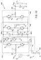
- Fig. 10 illustrates a power converter 700 according to another embodiment of the present invention, which resembles the embodiment of Fig. 5 with the addition of a battery coupling circuit 470 including seventh and eight switching transistors Q 7 , Q 8 that selectively couple a battery 460 to the first voltage bus 402a and the neutral bus N via a switch S B and an inductor L 4 .
- the switch S B which may be a mechanical or other switching device, is not required, but can reduce energy losses if opened when the battery 460 does not require charging.
- the first DC voltage V 1 preferably is controlled such that it never falls below the battery voltage V B .
- the switching actions of the first and second switching transistors Q 1 , Q 2 of the rectifier circuit 410 and/or the fifth and sixth switching transistors Q 5 , Q 6 of the balancer circuit 430 can control the first DC voltage V 1 .
- the seventh switching transistor Q 7 can be modulated (switched) to produce a current that charges the battery 460 .
- Fig. 11 is a waveform diagram illustrating exemplary operations for the embodiment of Fig. 10 when the battery 460 is charging.
- the seventh and eighth switching transistors Q 7 , Q 8 are switched to allow current to flow from the first voltage bus 402a to the battery 460 .
- the fifth and sixth switching transistors Q 5 , Q 6 of the balancer circuit 430 are each operated at 50% duty cycles for the time the magnitude of the input voltage V in is greater than the battery voltage V B .
- the seventh and eighth transistors Q 7 , Q 8 can be operated such that current does not flow between the battery 460 and the first voltage bus 402a during a positive half-cycle 1210 of the input voltage V in .
- the switch S B remains open, the operations of the balancer circuit 430 during the negative half -cycle 1220 of the input voltage V in can be changed from the operations described above with reference to Fig. 10 to provide more efficient operation while maintaining the first DC voltage V 1 at or above the battery voltage V B and prevent current flow therebetween. If the switch S B is opened, further improvement in efficiency can be gained, as the first DC voltage V 1 need no longer be constrained to be greater than or equal to the battery voltage V B .
- Fig. 13 illustrates a power converter 800 according to yet another embodiment of the present invention, wherein the inductance through which the fifth and sixth switching transistors Q 5 , Q 6 couple the neutral bus N to the first and second voltage busses 402a , 402b is provided by a first winding L a of a transformer T 1 .
- the fifth and sixth switching transistors Q 5 , Q 6 selectively couple the first and second voltage busses 402a , 402b to a first end tap of the winding L a , a center tap of the winding L a being coupled to the neutral bus N .
- a second end tap of the winding L a is coupled to a node between a serial-connected pair of diodes D 1 , D 2 coupled between the first and second voltage busses 402a , 402b .
- a secondary power source here a battery 460
- a secondary power source here a battery 460
- a battery 460 may be coupled to a second winding L b of the transformer T 1 via a switch S B and an AC voltage generating circuit 450 (e.g. a battery converter circuit).
- the switch S B is closed and the AC voltage generating circuit 450 produces an AC voltage (e.g., a square wave, quasi-square wave, sine wave, quasi sine wave, or other periodic or quasi-periodic voltage) across the second winding L b from a DC voltage produced by the battery 460 . This induces a corresponding AC voltage across the first winding L a .
- the fifth and sixth transistors Q 5 , Q 6 in conjunction with the diodes D 1 , D 2 , produce DC voltages V 1 , V 2 on the first and second voltage busses 402a , 402b from the AC voltage induced across the first winding L a .
- These DC voltages V 1 , V 2 may be inverted by the inverter 420 to produce an AC voltage at the output bus 403 .
- the battery 460 may be decoupled by opening the switch S B , as might be done when the converter 800 is operated as an off-line UPS.
- the AC voltage generating circuit 450 may act as a combined battery converter/battery charger circuit. In a battery charging mode, the AC voltage generating circuit 450 may act as a rectifier, producing a DC voltage across the battery 460 from an AC voltage induced on the second winding L b , thus allowing the battery 460 to be charged.
- An exemplary implementation for such dual purpose AC voltage generating circuit 450 is described with reference to Fig. 15, below.
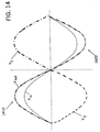
- Fig. 14 is waveform diagram illustrating exemplary operations for the converter 800 of Fig. 13 for a case in which the input voltage V in is boosted to produce a desired output voltage V out .
- the fifth and sixth switching transistors Q 5 , Q 6 are preferably both operated at 50% duty cycles in both positive and negative half-cycles 1410 , 1420 of the input voltage V in .
- the first and second DC voltages V 1 , V 2 are constrained to have substantially equal magnitudes.
- Fig. 14 illustrate another advantageous aspect of the balancer circuit 430 .
- Operating the fifth and sixth transistors Q 5 , Q 6 at 50% duty cycles can provide energy transfer from the second capacitor C 2 to the first capacitor C 1 during the positive half-cycle 1410 of the input voltage V in , helping maintain the first DC voltage V 1 when the load draws current.
- a similar energy transfer from the first capacitor C 1 to the second capacitor C 2 can be provided during the negative half-cycle 1420 of the input voltage V in . This ability to transfer energy allows the capacitors C 1 , C 2 to have a relatively low capacitance for a given power rating in comparison to storage capacitors used in many conventional converter designs.
- each of the capacitors C 1 , C 2 allows each of the capacitors C 1 , C 2 to have a "per unit" capacitance of less than 1.
- Per unit capacitance may be described as follows. If nominal AC voltage is applied across one of the capacitors C 1 , C 2 , the capacitor would draw an AC current proportional to its capacitance. If this current is equal to a full load AC current for the power converter 400 at the nominal AC voltage, the capacitor may be described as having per unit capacitance of 1. If the current drawn at the nominal AC voltage is less than the full load AC current for the power converter 800 , however, the capacitor would have a per unit capacitance that is less than 1.
- Fig. 13 utilizes a half-bridge configuration, and that similar functionality may be achieved using a full-bridge configuration.
- the diodes D 1 , D 2 of Fig. 13 may be replaced by seventh and eighth switching transistors Q 7 , Q 8 , the switching operations of which may be controlled, for example, by a switch control circuit along the lines of the switch control circuit 440 of Fig. 5.
- the embodiments of Figs. 13 and 15 represent exemplary implementations, and that other circuit implementations fall within the scope of the present invention.
- the switching functions of the transistors Q 1 , Q 2 , Q 3 , Q 4 , Q 5 , Q 9 , Q 7 , Q 8 may be provided by a variety of switching devices, such as those described above with reference to Fig. 5, controlled using any of a number of different control circuit implementations, such as those described above with reference to Fig. 5.
- Fig. 16 illustrates an exemplary implementation of an AC voltage generating circuit 450 that may also act as a combined battery converter/battery charger circuit.
- the AC voltage generating circuit 450 includes four switching transistors Q a , Q b , Q c , Q d connected in a bridge configuration between the transformer winding L b and the battery 460 .
- the transistors Q a , Q b , Q c , Q d are controlled by a switch control circuit 452 .
- a current limiting inductor L cl is connected in series with the battery 460 and the switch S B , and a storage capacitor C S is connected across the series combination.
- the switch control circuit 452 may control switching operations of the transistors Q a , Q b , Q c , Q d responsive to a variety of state inputs, such as a sensed voltage of the battery 460 , and sensed AC input and output voltages for a battery converter in which the AC voltage generating circuit 450 is included.
- the switch control circuit 452 may be operated to selectively switch the transistors Q a , Q b , Q c , Q d such that a DC voltage produced by the battery 460 across the storage capacitor C S is inverted, producing an AC voltage across the winding L b . This may be achieved, for example, by switching a first pair of transistors Q a , Q b , in a complementary pattern to a second pair of transistors Q c , Q d at the desired AC line frequency.
- an AC voltage may be applied to the first winding L a of the transformer T 1 by action of the fifth and sixth transistors 431 , 432 of the balancer circuit 430 , inducing an AC voltage on the second winding L b .
- the switch control circuit 452 may selectively switch the transistors Q a , Q b , Q c , Q d such that the AC voltage induced on the winding L b is rectified to produce a DC voltage across the storage capacitor C S that can be used to charge the battery 460 .
- the magnitude of the voltage across the battery 460 can be controlled by the manner in which the transistors Q a , Q b , Q c , Q d are operated, such that when the battery approaches a full charge the current flowing into the battery 460 can be reduced to avoid overcharging.
- the switch S B can be opened.
- Fig. 16 represents an exemplary implementation, and that other circuit implementations fall within the scope of the present invention.
- the switching functions of the transistors Q a , Q b , Q c , Q d may be provided by any of a number of different switching devices such as those described in relation to Fig. 5, controlled using any of a number of different implementations of the switch control circuit 452 , such as ones similar to those described for the switch control circuit 440 of Fig. 5.
- functions of the switch control circuits 440 , 452 of Figs. 5 and 16 may also be combined in one or more devices. It will further be understood that although the battery converter/battery charger circuit illustrated in 450 of Fig.
- circuit 16 is capable of a combined rectifier/inverter operation in order provide battery charging in addition to generation of an AC voltage across the winding L b
- circuit implementations of the AC voltage generating circuit 450 which provide only inversion of the DC voltage produced by the battery may also be used with the present invention.
- Such a circuit may provide battery charging via an ancillary battery charging circuit (not shown).
Landscapes
- Engineering & Computer Science (AREA)
- Power Engineering (AREA)
- Business, Economics & Management (AREA)
- Emergency Management (AREA)
- Inverter Devices (AREA)
- Stand-By Power Supply Arrangements (AREA)
- Rectifiers (AREA)
Applications Claiming Priority (2)
| Application Number | Priority Date | Filing Date | Title |
|---|---|---|---|
| US37418099A | 1999-08-13 | 1999-08-13 | |
| US374180 | 1999-08-13 |
Publications (2)
| Publication Number | Publication Date |
|---|---|
| EP1076403A2 true EP1076403A2 (de) | 2001-02-14 |
| EP1076403A3 EP1076403A3 (de) | 2002-01-02 |
Family
ID=23475661
Family Applications (1)
| Application Number | Title | Priority Date | Filing Date |
|---|---|---|---|
| EP00115097A Withdrawn EP1076403A3 (de) | 1999-08-13 | 2000-07-27 | Leistungswandler mit mehreren Betriebsarten und Ausgleichsschaltungen und zugehöriges Betriebsverfahren |
Country Status (9)
| Country | Link |
|---|---|
| US (2) | US6160722A (de) |
| EP (1) | EP1076403A3 (de) |
| JP (1) | JP2001086765A (de) |
| CN (1) | CN1284777A (de) |
| AU (1) | AU764387B2 (de) |
| BR (1) | BR0003570A (de) |
| CA (1) | CA2314782C (de) |
| DE (1) | DE1076403T1 (de) |
| MX (1) | MXPA00007910A (de) |
Cited By (5)
| Publication number | Priority date | Publication date | Assignee | Title |
|---|---|---|---|---|
| WO2007035392A3 (en) * | 2005-09-19 | 2007-06-21 | Skyworks Solutions Inc | Switched mode power converter |
| US7561453B2 (en) | 2004-07-12 | 2009-07-14 | Siemens Ag Osterreich | Method for operating an inverter and arrangement for executing the method |
| EP2846436A4 (de) * | 2013-07-05 | 2015-07-08 | Huawei Tech Co Ltd | Schaltung für eine ununterbrochene stromversorgung |
| EP3503366A1 (de) * | 2017-12-25 | 2019-06-26 | Delta Electronics, Inc. | Unterbrechungsfreie stromversorgungsvorrichtung |
| EP3683943A1 (de) * | 2019-01-17 | 2020-07-22 | Cotek Electronic Ind. Co., Ltd. | Stromwandler |
Families Citing this family (182)
| Publication number | Priority date | Publication date | Assignee | Title |
|---|---|---|---|---|
| AU2432701A (en) | 1999-12-16 | 2001-06-25 | Mcandrews Enterprises Inc. | Spare bus power plant |
| EP2083498B1 (de) * | 2000-01-28 | 2010-12-08 | Cummins Generator Technologies Limited | Wechselstromerzeugungssystem |
| US20010045779A1 (en) * | 2000-05-26 | 2001-11-29 | Huey Lee | Intelligent power system |
| JP2003535563A (ja) | 2000-05-31 | 2003-11-25 | シュア パワー コーポレーション | Dcバスを用いた電源システム |
| US6603672B1 (en) * | 2000-11-10 | 2003-08-05 | Ballard Power Systems Corporation | Power converter system |
| DE10103144A1 (de) * | 2001-01-24 | 2002-08-01 | Infineon Technologies Ag | Halbbrückenschaltung |
| US6605879B2 (en) * | 2001-04-19 | 2003-08-12 | Powerware Corporation | Battery charger control circuit and an uninterruptible power supply utilizing same |
| JP2004528798A (ja) * | 2001-06-05 | 2004-09-16 | コーニンクレッカ フィリップス エレクトロニクス エヌ ヴィ | パワーオンおよびパワーオフ制御シーケンスをもつ電源アーキテクチャ |
| EP1276202B1 (de) * | 2001-06-26 | 2008-01-09 | Sanyo Denki Co., Ltd. | Unterbrechungsfreie Stromversorgung und Verfahren zum Ausschalten eines Wechselstromschalters für eine Unterbrechungsfreie Stromversorgung |
| WO2003032466A1 (fr) * | 2001-10-03 | 2003-04-17 | Mitsubishi Denki Kabushiki Kaisha | Alimentation electrique sans coupure et procede de demarrage de celle-ci |
| US20030076696A1 (en) * | 2001-10-18 | 2003-04-24 | Delta Electronics, Inc. | Device of uninterruptible power supply |
| CN100541994C (zh) * | 2002-03-25 | 2009-09-16 | 电力设备公司 | 利用平衡器电路的电源变换设备和方法 |
| KR20030083374A (ko) * | 2002-04-22 | 2003-10-30 | 유지고하라 | 직류전류의 불변동분할을 가능하도록한 에너지 절약장치 |
| WO2003103110A1 (en) * | 2002-06-04 | 2003-12-11 | Sure Power Corporation | Load break dc power disconnect |
| CN1333506C (zh) * | 2002-08-14 | 2007-08-22 | 艾默生网络能源有限公司 | 带母线均压功能的不间断电源系统 |
| US7105948B2 (en) * | 2002-09-10 | 2006-09-12 | Abb Schweiz Ag | Apparatus for the voltage maintenance of an electrical AC voltage supply network and method for operating such an apparatus |
| US7545120B2 (en) * | 2003-07-29 | 2009-06-09 | Dell Products L.P. | AC-DC adapter and battery charger integration for portable information handling systems |
| US7592716B2 (en) * | 2003-07-29 | 2009-09-22 | Dell Products L.P. | Information handling system including a battery that reduces a voltage fluctuation |
| US7084525B2 (en) * | 2003-08-28 | 2006-08-01 | Delphi Technologies, Inc. | Power system to transfer power between a plurality of power sources |
| US7049870B2 (en) * | 2004-01-09 | 2006-05-23 | Potentia Semiconductor Corporation | Digital controllers for DC converters |
| US7684222B2 (en) * | 2004-03-24 | 2010-03-23 | Eaton Corporation | Power conversion apparatus with DC bus precharge circuits and methods of operation thereof |
| US7333349B2 (en) * | 2004-03-31 | 2008-02-19 | University Of New Brunswick | Single-stage buck-boost inverter |
| JP4556516B2 (ja) * | 2004-07-08 | 2010-10-06 | 富士電機システムズ株式会社 | 電力変換装置 |
| US7391188B2 (en) * | 2004-08-02 | 2008-06-24 | Jacobs James K | Current prediction in a switching power supply |
| US20060132111A1 (en) * | 2004-08-02 | 2006-06-22 | Jacobs James K | Power supply with multiple modes of operation |
| US7391132B2 (en) * | 2004-12-03 | 2008-06-24 | Huei-Jung Chen | Methods and apparatus providing double conversion/series-parallel hybrid operation in uninterruptible power supplies |
| US7208891B2 (en) * | 2005-05-06 | 2007-04-24 | York International Corp. | Variable speed drive for a chiller system |
| JP2006313487A (ja) * | 2005-05-09 | 2006-11-16 | Hitachi Ltd | ディスクアレイ装置 |
| EP1722387B1 (de) * | 2005-05-13 | 2008-01-02 | Abb Research Ltd. | Elektronische Schaltungsanordnung für Regelzwecke |
| US7382114B2 (en) | 2005-06-07 | 2008-06-03 | Intersil Americas Inc. | PFM-PWM DC-DC converter providing DC offset correction to PWM error amplifier and equalizing regulated voltage conditions when transitioning between PFM and PWM modes |
| US7332885B2 (en) * | 2005-09-02 | 2008-02-19 | Johnson Controls Technology Company | Ride-through method and system for HVAC&R chillers |
| US7081734B1 (en) | 2005-09-02 | 2006-07-25 | York International Corporation | Ride-through method and system for HVACandR chillers |
| US11881814B2 (en) | 2005-12-05 | 2024-01-23 | Solaredge Technologies Ltd. | Testing of a photovoltaic panel |
| US10693415B2 (en) | 2007-12-05 | 2020-06-23 | Solaredge Technologies Ltd. | Testing of a photovoltaic panel |
| US20070151272A1 (en) * | 2006-01-03 | 2007-07-05 | York International Corporation | Electronic control transformer using DC link voltage |
| EP1806819A1 (de) * | 2006-01-05 | 2007-07-11 | Constructions Electroniques + Telecommunications, en abrégé "C.E.+T" | Reservestromversorgung |
| US7508094B2 (en) * | 2006-03-17 | 2009-03-24 | Eaton Corporation | UPS systems having multiple operation modes and methods of operating same |
| US7869771B2 (en) * | 2006-06-23 | 2011-01-11 | Broadcom Corporation | Multi-band transformer for wireless transmitter |
| US8280325B2 (en) * | 2006-06-23 | 2012-10-02 | Broadcom Corporation | Configurable transmitter |
| TWI315118B (en) * | 2006-07-12 | 2009-09-21 | Delta Electronics Inc | Method for controlling uninterruptible power supply apparatus |
| US7336513B1 (en) | 2006-09-12 | 2008-02-26 | National Chung Cheng University | Method of compensating output voltage distortion of half-bridge inverter and device based on the method |
| US9071168B2 (en) * | 2006-09-25 | 2015-06-30 | Voltwerk Electronics Gmbh | Power inverter circuit for adjusting symmetry of the AC-voltage without load-coupling |
| US7710081B2 (en) | 2006-10-27 | 2010-05-04 | Direct Drive Systems, Inc. | Electromechanical energy conversion systems |
| US8947194B2 (en) | 2009-05-26 | 2015-02-03 | Solaredge Technologies Ltd. | Theft detection and prevention in a power generation system |
| US11735910B2 (en) | 2006-12-06 | 2023-08-22 | Solaredge Technologies Ltd. | Distributed power system using direct current power sources |
| US11309832B2 (en) | 2006-12-06 | 2022-04-19 | Solaredge Technologies Ltd. | Distributed power harvesting systems using DC power sources |
| US8816535B2 (en) | 2007-10-10 | 2014-08-26 | Solaredge Technologies, Ltd. | System and method for protection during inverter shutdown in distributed power installations |
| US8473250B2 (en) | 2006-12-06 | 2013-06-25 | Solaredge, Ltd. | Monitoring of distributed power harvesting systems using DC power sources |
| US11888387B2 (en) | 2006-12-06 | 2024-01-30 | Solaredge Technologies Ltd. | Safety mechanisms, wake up and shutdown methods in distributed power installations |
| US11569659B2 (en) | 2006-12-06 | 2023-01-31 | Solaredge Technologies Ltd. | Distributed power harvesting systems using DC power sources |
| US8963369B2 (en) | 2007-12-04 | 2015-02-24 | Solaredge Technologies Ltd. | Distributed power harvesting systems using DC power sources |
| US8013472B2 (en) | 2006-12-06 | 2011-09-06 | Solaredge, Ltd. | Method for distributed power harvesting using DC power sources |
| US8618692B2 (en) | 2007-12-04 | 2013-12-31 | Solaredge Technologies Ltd. | Distributed power system using direct current power sources |
| US11855231B2 (en) | 2006-12-06 | 2023-12-26 | Solaredge Technologies Ltd. | Distributed power harvesting systems using DC power sources |
| US8384243B2 (en) | 2007-12-04 | 2013-02-26 | Solaredge Technologies Ltd. | Distributed power harvesting systems using DC power sources |
| US8319483B2 (en) | 2007-08-06 | 2012-11-27 | Solaredge Technologies Ltd. | Digital average input current control in power converter |
| US9088178B2 (en) | 2006-12-06 | 2015-07-21 | Solaredge Technologies Ltd | Distributed power harvesting systems using DC power sources |
| US8319471B2 (en) | 2006-12-06 | 2012-11-27 | Solaredge, Ltd. | Battery power delivery module |
| US11687112B2 (en) | 2006-12-06 | 2023-06-27 | Solaredge Technologies Ltd. | Distributed power harvesting systems using DC power sources |
| US12316274B2 (en) | 2006-12-06 | 2025-05-27 | Solaredge Technologies Ltd. | Pairing of components in a direct current distributed power generation system |
| US8495890B2 (en) * | 2007-01-22 | 2013-07-30 | Johnson Controls Technology Company | Cooling member |
| US8014110B2 (en) | 2007-01-22 | 2011-09-06 | Johnson Controls Technology Company | Variable speed drive with integral bypass contactor |
| US8149579B2 (en) * | 2008-03-28 | 2012-04-03 | Johnson Controls Technology Company | Cooling member |
| US7800924B2 (en) * | 2007-03-27 | 2010-09-21 | Eaton Corporation | Power converter apparatus and methods using neutral coupling circuits with interleaved operation |
| WO2008137276A1 (en) | 2007-05-08 | 2008-11-13 | Johnson Controls Technology Company | Variable speed drive |
| US7573732B2 (en) * | 2007-05-25 | 2009-08-11 | General Electric Company | Protective circuit and method for multi-level converter |
| CN101904073B (zh) | 2007-10-15 | 2014-01-08 | Ampt有限公司 | 高效太阳能电力系统 |
| WO2009055474A1 (en) * | 2007-10-23 | 2009-04-30 | And, Llc | High reliability power systems and solar power converters |
| CN101836342B (zh) * | 2007-10-22 | 2013-02-06 | 西门子公司 | 用于连接动态定位的船舶中的发电机和推进器的电气开关设备及其运行方法 |
| US7957166B2 (en) * | 2007-10-30 | 2011-06-07 | Johnson Controls Technology Company | Variable speed drive |
| US8174853B2 (en) * | 2007-10-30 | 2012-05-08 | Johnson Controls Technology Company | Variable speed drive |
| US8049523B2 (en) | 2007-12-05 | 2011-11-01 | Solaredge Technologies Ltd. | Current sensing on a MOSFET |
| US11264947B2 (en) | 2007-12-05 | 2022-03-01 | Solaredge Technologies Ltd. | Testing of a photovoltaic panel |
| EP3496258B1 (de) | 2007-12-05 | 2025-02-05 | Solaredge Technologies Ltd. | Sicherheitsmechanismus in verteilten strominstallationen |
| TW200934032A (en) * | 2008-01-30 | 2009-08-01 | Tsann Kuen Entpr Co Ltd | Induction type electrical power supply |
| TW200935704A (en) * | 2008-02-01 | 2009-08-16 | Tsann Kuen Entpr Co Ltd | Induction type electrical power structure and system |
| US7759900B2 (en) * | 2008-04-02 | 2010-07-20 | American Power Conversion Corporation | Non-isolated charger with bi-polar inputs |
| US20090256534A1 (en) * | 2008-04-14 | 2009-10-15 | Twisthink, L.L.C. | Power supply control method and apparatus |
| EP3121922B1 (de) | 2008-05-05 | 2020-03-04 | Solaredge Technologies Ltd. | Gleichstromleistungskombinierer |
| JP5190683B2 (ja) * | 2008-06-11 | 2013-04-24 | サンケン電気株式会社 | 交流電源装置 |
| US8040007B2 (en) | 2008-07-28 | 2011-10-18 | Direct Drive Systems, Inc. | Rotor for electric machine having a sleeve with segmented layers |
| JP5248611B2 (ja) | 2008-07-30 | 2013-07-31 | 東芝三菱電機産業システム株式会社 | 電力変換装置 |
| US8884201B2 (en) * | 2008-09-15 | 2014-11-11 | The Boeing Company | Systems and methods for fabrication of thermoplastic components |
| US8336323B2 (en) * | 2008-10-03 | 2012-12-25 | Johnson Controls Technology Company | Variable speed drive with pulse-width modulated speed control |
| WO2010042124A1 (en) * | 2008-10-10 | 2010-04-15 | Ampt, Llc | Novel solar power circuits and powering methods |
| RU2426215C2 (ru) * | 2008-12-03 | 2011-08-10 | Федеральное космическое агентство Федеральное государственное унитарное предприятие НАУЧНО-ПРОИЗВОДСТВЕННОЕ ПРЕДПРИЯТИЕ ВСЕРОССИЙСКИЙ НАУЧНО-ИССЛЕДОВАТЕЛЬСКИЙ ИНСТИТУТ ЭЛЕКТРОМЕХАНИКИ С ЗАВОДОМ имени А.Г. ИОСИФЬЯНА НПП ВНИИЭМ | Источник бесперебойного питания потребителей переменного тока |
| US8212402B2 (en) | 2009-01-27 | 2012-07-03 | American Power Conversion Corporation | System and method for limiting losses in an uninterruptible power supply |
| WO2010111433A2 (en) | 2009-03-25 | 2010-09-30 | Powergetics, Inc. | Bidirectional energy converter |
| JP5374210B2 (ja) * | 2009-03-31 | 2013-12-25 | 本田技研工業株式会社 | Dc/dcコンバータおよびそれを用いた給電システム |
| US9442504B2 (en) | 2009-04-17 | 2016-09-13 | Ampt, Llc | Methods and apparatus for adaptive operation of solar power systems |
| US8604384B2 (en) | 2009-06-18 | 2013-12-10 | Illinois Tool Works Inc. | System and methods for efficient provision of arc welding power source |
| EP2449652A4 (de) | 2009-06-29 | 2014-08-13 | Stem Inc | Hochgeschwindigkeits-feedback zur stromladungsreduzierung mithilfe eines variablen generators |
| WO2011008505A2 (en) * | 2009-06-29 | 2011-01-20 | Powergetics, Inc | High speed feedback adjustment of power charge/discharge from energy storage system |
| US9466737B2 (en) | 2009-10-19 | 2016-10-11 | Ampt, Llc | Solar panel string converter topology |
| US12418177B2 (en) | 2009-10-24 | 2025-09-16 | Solaredge Technologies Ltd. | Distributed power system using direct current power sources |
| US8148942B2 (en) * | 2009-11-05 | 2012-04-03 | O2Micro International Limited | Charging systems with cell balancing functions |
| US8575778B2 (en) * | 2010-01-12 | 2013-11-05 | Ford Global Technologies, Llc | Variable voltage converter (VVC) with integrated battery charger |
| KR101131664B1 (ko) * | 2010-01-28 | 2012-03-28 | 장석호 | 스위칭 배열과 충방전을 이용한 고효율 충전장치 |
| DE102010003797A1 (de) * | 2010-04-09 | 2011-10-13 | Tridonic Ag | Modulares LED-Beleuchtungssystem mit Notlichtfunktion |
| US20120074786A1 (en) | 2010-05-13 | 2012-03-29 | Eaton Corporation | Uninterruptible power supply systems and methods using isolated interface for variably available power source |
| CN102005938B (zh) * | 2010-08-25 | 2013-01-30 | 力博特公司 | Ups中的桥臂过零工作时的控制方法 |
| US8760078B2 (en) * | 2010-10-04 | 2014-06-24 | Earl W. McCune, Jr. | Power conversion and control systems and methods for solid-state lighting |
| GB2485527B (en) | 2010-11-09 | 2012-12-19 | Solaredge Technologies Ltd | Arc detection and prevention in a power generation system |
| US10673222B2 (en) | 2010-11-09 | 2020-06-02 | Solaredge Technologies Ltd. | Arc detection and prevention in a power generation system |
| US10673229B2 (en) | 2010-11-09 | 2020-06-02 | Solaredge Technologies Ltd. | Arc detection and prevention in a power generation system |
| US10230310B2 (en) | 2016-04-05 | 2019-03-12 | Solaredge Technologies Ltd | Safety switch for photovoltaic systems |
| US9312705B2 (en) | 2010-12-22 | 2016-04-12 | Ge Energy Power Conversion Technology Limited | Capacitor balancing circuit and control method for an electronic device such as a multilevel power inverter |
| EP2656496B1 (de) | 2010-12-22 | 2019-09-11 | GE Energy Power Conversion Technology Limited | Mechanische anordnung einer mehrstufigen stromrichterschaltungsanordnung |
| GB2483317B (en) | 2011-01-12 | 2012-08-22 | Solaredge Technologies Ltd | Serially connected inverters |
| US8854004B2 (en) * | 2011-01-12 | 2014-10-07 | Samsung Sdi Co., Ltd. | Energy storage system and controlling method thereof |
| US8816533B2 (en) * | 2011-02-16 | 2014-08-26 | Eaton Corporation | Uninterruptible power supply systems and methods using an isolated neutral reference |
| US8730691B2 (en) | 2011-05-11 | 2014-05-20 | Eaton Corporation | Power conversion apparatus and methods employing variable-level inverters |
| JP5800130B2 (ja) * | 2011-06-20 | 2015-10-28 | 富士電機株式会社 | 直流電源システム |
| US8570005B2 (en) | 2011-09-12 | 2013-10-29 | Solaredge Technologies Ltd. | Direct current link circuit |
| US9106103B2 (en) | 2011-09-23 | 2015-08-11 | Eaton Corporation | Unintteruptible power supply systems and methods employing on-demand energy storage |
| US8774977B2 (en) | 2011-12-29 | 2014-07-08 | Stem, Inc. | Multiphase electrical power construction and assignment at minimal loss |
| US8803570B2 (en) | 2011-12-29 | 2014-08-12 | Stem, Inc | Multiphase electrical power assignment at minimal loss |
| US8922192B2 (en) | 2011-12-30 | 2014-12-30 | Stem, Inc. | Multiphase electrical power phase identification |
| GB2498365A (en) | 2012-01-11 | 2013-07-17 | Solaredge Technologies Ltd | Photovoltaic module |
| GB2498791A (en) | 2012-01-30 | 2013-07-31 | Solaredge Technologies Ltd | Photovoltaic panel circuitry |
| GB2498790A (en) | 2012-01-30 | 2013-07-31 | Solaredge Technologies Ltd | Maximising power in a photovoltaic distributed power system |
| US9853565B2 (en) | 2012-01-30 | 2017-12-26 | Solaredge Technologies Ltd. | Maximized power in a photovoltaic distributed power system |
| FR2986917B1 (fr) * | 2012-02-13 | 2014-02-21 | Converteam Technology Ltd | Systeme d'alimentation electrique d'une charge, et centrale de production d'energie electrique comprenant un tel systeme |
| GB2499991A (en) | 2012-03-05 | 2013-09-11 | Solaredge Technologies Ltd | DC link circuit for photovoltaic array |
| JP5403090B2 (ja) * | 2012-03-09 | 2014-01-29 | 富士電機株式会社 | 電力変換装置 |
| JP5370519B2 (ja) * | 2012-03-15 | 2013-12-18 | 富士電機株式会社 | 電力変換装置 |
| EP2647523A1 (de) * | 2012-04-04 | 2013-10-09 | Volvo Car Corporation | Schaltung zum Laden einer Batterie und Ansteuerverfahren einer Drehstrommaschine |
| US9444320B1 (en) * | 2012-04-16 | 2016-09-13 | Performance Controls, Inc. | Power controller having active voltage balancing of a power supply |
| CN102710006B (zh) * | 2012-05-18 | 2014-12-24 | 深圳市健网科技有限公司 | 一种带平衡桥臂的双电源供电系统 |
| WO2014011706A1 (en) | 2012-07-09 | 2014-01-16 | Inertech Ip Llc | Transformerless multi-level medium-voltage uninterruptible power supply (ups) systems and methods |
| US9490663B1 (en) * | 2012-07-16 | 2016-11-08 | Google Inc. | Apparatus and methodology for battery backup circuit and control in an uninterruptible power supply |
| US9406094B2 (en) | 2012-08-14 | 2016-08-02 | Stem Inc. | Method and apparatus for delivering power using external data |
| US10782721B2 (en) | 2012-08-27 | 2020-09-22 | Stem, Inc. | Method and apparatus for balancing power on a per phase basis in multi-phase electrical load facilities using an energy storage system |
| US11454999B2 (en) | 2012-08-29 | 2022-09-27 | Stem, Inc. | Method and apparatus for automatically reconfiguring multi-phased networked energy storage devices at a site |
| RU2513547C1 (ru) * | 2012-09-07 | 2014-04-20 | Общество с ограниченной ответственностью "Гамем" (ООО Гамем") | Статический обратимый преобразователь для питания потребителей переменного и постоянного тока |
| US10756543B2 (en) | 2012-09-13 | 2020-08-25 | Stem, Inc. | Method and apparatus for stabalizing power on an electrical grid using networked distributed energy storage systems |
| US9634508B2 (en) | 2012-09-13 | 2017-04-25 | Stem, Inc. | Method for balancing frequency instability on an electric grid using networked distributed energy storage systems |
| US10389126B2 (en) | 2012-09-13 | 2019-08-20 | Stem, Inc. | Method and apparatus for damping power oscillations on an electrical grid using networked distributed energy storage systems |
| US10693294B2 (en) | 2012-09-26 | 2020-06-23 | Stem, Inc. | System for optimizing the charging of electric vehicles using networked distributed energy storage systems |
| CN102882256B (zh) * | 2012-10-12 | 2015-11-11 | 广东易事特电源股份有限公司 | 一种具有双母线充电电路的ups电源 |
| US9246411B2 (en) * | 2012-10-16 | 2016-01-26 | Rockwell Automation Technologies, Inc. | Regenerative voltage doubler rectifier, voltage sag/swell correction apparatus and operating methods |
| RU2505917C1 (ru) * | 2012-11-01 | 2014-01-27 | Федеральное государственное бюджетное образовательное учреждение высшего профессионального образования "Национальный минерально-сырьевой университет "Горный" | Система автономного электроснабжения |
| WO2014082221A1 (en) * | 2012-11-28 | 2014-06-05 | Eaton Corporation | Multi-level converter apparatus with efficiency improving current bypass |
| US9548619B2 (en) | 2013-03-14 | 2017-01-17 | Solaredge Technologies Ltd. | Method and apparatus for storing and depleting energy |
| US9941813B2 (en) | 2013-03-14 | 2018-04-10 | Solaredge Technologies Ltd. | High frequency multi-level inverter |
| US9397497B2 (en) | 2013-03-15 | 2016-07-19 | Ampt, Llc | High efficiency interleaved solar power supply system |
| US9537332B2 (en) | 2013-05-30 | 2017-01-03 | Canara, Inc. | Apparatus, system and method for charge balancing of individual batteries in a string of batteries using battery voltage and temperature, and detecting and preventing thermal runaway |
| CN203674762U (zh) * | 2014-01-09 | 2014-06-25 | 成都芯源系统有限公司 | 移动电源电路 |
| CN104882913A (zh) * | 2014-02-27 | 2015-09-02 | 伊顿制造(格拉斯哥)有限合伙莫尔日分支机构 | 一种ups电路 |
| US9318974B2 (en) | 2014-03-26 | 2016-04-19 | Solaredge Technologies Ltd. | Multi-level inverter with flying capacitor topology |
| CN104092277A (zh) * | 2014-04-23 | 2014-10-08 | 矽力杰半导体技术(杭州)有限公司 | 包含双向直流变换器的电源电路及其控制方法 |
| CN106464002B (zh) * | 2014-05-02 | 2020-09-08 | 施耐德电气It公司 | 不间断电源系统及其操作方法 |
| EP3210297B1 (de) | 2014-10-21 | 2021-03-10 | Inertech IP LLC | Systeme und verfahren zur steuerung mehrstufiger diodenklemmen-wechselrichter mit raumvektor-pulsweitenmodulation (svpwm) |
| US9479004B2 (en) * | 2015-03-13 | 2016-10-25 | Active-Semi, Inc. | Buck/boost circuit that charges and discharges multi-cell batteries of a power bank device |
| US10120034B2 (en) | 2015-10-07 | 2018-11-06 | Canara, Inc. | Battery string monitoring system |
| US10931190B2 (en) | 2015-10-22 | 2021-02-23 | Inertech Ip Llc | Systems and methods for mitigating harmonics in electrical systems by using active and passive filtering techniques |
| US10734918B2 (en) | 2015-12-28 | 2020-08-04 | Illinois Tool Works Inc. | Systems and methods for efficient provision of arc welding power source |
| US12057807B2 (en) | 2016-04-05 | 2024-08-06 | Solaredge Technologies Ltd. | Chain of power devices |
| US11018623B2 (en) | 2016-04-05 | 2021-05-25 | Solaredge Technologies Ltd. | Safety switch for photovoltaic systems |
| US11177663B2 (en) | 2016-04-05 | 2021-11-16 | Solaredge Technologies Ltd. | Chain of power devices |
| US10574086B2 (en) * | 2016-04-08 | 2020-02-25 | Rhombus Energy Solutions, Inc. | Nonlinear control algorithm and system for a single-phase AC-AC converter with bidirectional isolated DC-DC converter |
| US10454381B2 (en) * | 2016-09-15 | 2019-10-22 | Virginia Tech Intellectual Properties, Inc. | Variable DC link converter and transformer for wide output voltage range applications |
| US10811987B2 (en) * | 2017-03-31 | 2020-10-20 | Schneider Electric It Corporation | Bi-directional DC-DC converter with load and source synchronized power control |
| RU180664U1 (ru) * | 2017-05-30 | 2018-06-20 | Общество С Ограниченной Ответственностью Научно-Производственное Предприятие "Томская Электронная Компания" | Источник бесперебойного энергоснабжения |
| RU191898U1 (ru) * | 2018-02-20 | 2019-08-27 | Общество с ограниченной ответственностью "АЕДОН" | Модульный вторичный источник питания |
| US10536092B1 (en) | 2018-03-02 | 2020-01-14 | Apple Inc. | Symmetric hybrid converters |
| RU186995U1 (ru) * | 2018-06-07 | 2019-02-12 | Общество с ограниченной ответственностью "АСХ" (ООО "АСХ") | Исполнительное устройство преимущественно для автоматизированной системы сбора данных с приборов учета и управления ресурсами в жилищно-коммунальном хозяйстве |
| WO2020051557A1 (en) | 2018-09-06 | 2020-03-12 | Cornell University | High power density power converter and uninterruptible power supply circuit and methods |
| CN111181390A (zh) * | 2018-11-13 | 2020-05-19 | 深圳市贝贝特科技实业有限公司 | 一种电路均衡器及无人机 |
| TWI690144B (zh) * | 2018-11-14 | 2020-04-01 | 國家中山科學研究院 | 三臂式整流與變流電路 |
| CN111342677A (zh) * | 2018-12-18 | 2020-06-26 | 协欣电子工业股份有限公司 | 电力转换器 |
| RU187091U1 (ru) * | 2018-12-20 | 2019-02-19 | Федеральное государственное бюджетное образовательное учреждение высшего образования "Национальный исследовательский Мордовский государственный университет им. Н.П. Огарёва" | Устройство управления трехфазным выпрямительно-инверторным модулем |
| EP3672054B1 (de) | 2018-12-21 | 2021-06-16 | Eltek AS | Energieumwandler und verfahren zur steuerung von energieumwandlung |
| CN112436723B (zh) * | 2019-08-09 | 2022-02-22 | 株洲中车时代电气股份有限公司 | 一种抑制牵引主电路中间电压震荡的方法及牵引主电路 |
| US11157430B2 (en) * | 2019-12-19 | 2021-10-26 | Schneider Electric It Corporation | DC-DC power converter with four way power conversion |
| RU2732280C1 (ru) * | 2019-12-26 | 2020-09-15 | Акционерное общество "Научно-производственная корпорация "Космические системы мониторинга, информационно-управляющие и электромеханические комплексы" имени А.Г. Иосифьяна" АО "Корпорация "ВНИИЭМ" | Источник бесперебойного питания - статический обратимый преобразователь для питания потребителей переменного и постоянного тока и заряда (подзаряда) аккумуляторной батареи |
| GB2586343B (en) * | 2020-07-07 | 2024-03-13 | Zhong Qingchang | Power electronic converter with a ground fault detection unit that shares a common ground with both DC ports and AC ports |
| KR102379157B1 (ko) * | 2020-11-04 | 2022-03-25 | 한국항공우주연구원 | 통합형 dc/dc 및 ac/dc 컨버터 시스템 |
| RU203769U1 (ru) * | 2020-12-17 | 2021-04-21 | Общество с ограниченной ответственностью Научно-производственное предприятие «Томская электронная компания» | Источник бесперебойного электропитания |
| US11374501B1 (en) * | 2021-03-26 | 2022-06-28 | Product Development Associates, Inc. | Phase balancer including power conversion circuits |
| TWI794926B (zh) * | 2021-08-12 | 2023-03-01 | 台達電子工業股份有限公司 | 接地故障偵測裝置及其接地故障偵測方法 |
| CN115776241B (zh) * | 2022-06-23 | 2023-07-21 | 中国科学院电工研究所 | 基于开关单元的ac-ac变换器及控制方法 |
Family Cites Families (27)
| Publication number | Priority date | Publication date | Assignee | Title |
|---|---|---|---|---|
| US3775663A (en) * | 1972-08-24 | 1973-11-27 | Gen Electric | Inverter with electronically controlled neutral terminal |
| US4507724A (en) * | 1983-10-17 | 1985-03-26 | Sundstrand Corporation | Pulse width modulated inverter for unbalanced and variable power factor loads |
| US4502106A (en) * | 1983-10-17 | 1985-02-26 | Sundstrand Corporation | Current source sine wave inverter |
| FI81465C (fi) | 1986-12-22 | 1990-10-10 | Kone Oy | Anordning foer kopplandet av ett ackumulatorbatteri till en hissinverters likstroemskrets. |
| US5237208A (en) * | 1988-10-25 | 1993-08-17 | Nishimu Electronics Industries Co., Ltd. | Apparatus for parallel operation of triport uninterruptable power source devices |
| US5017800A (en) * | 1989-09-29 | 1991-05-21 | Wisconsin Alumni Research Foundation | AC to DC to AC power conversion apparatus with few active switches and input and output control |
| US5126585A (en) * | 1990-06-19 | 1992-06-30 | Auckland Uniservices Limited | Uninterruptible power supplies |
| US5111374A (en) * | 1990-06-22 | 1992-05-05 | The University Of Tennessee Research Corp. | High frequency quasi-resonant DC voltage notching scheme of a PWM voltage fed inverter for AC motor drives |
| US5111376A (en) * | 1990-11-01 | 1992-05-05 | Sundstrand Corporation | Voltage balancing circuit |
| US5229650A (en) * | 1990-11-07 | 1993-07-20 | Yuasa Battery Company Limited | Uniterruptible power system |
| US5343079A (en) | 1991-02-25 | 1994-08-30 | Regents Of The University Of Minnesota | Standby power supply with load-current harmonics neutralizer |
| US5119283A (en) * | 1991-06-10 | 1992-06-02 | General Electric Company | High power factor, voltage-doubler rectifier |
| US5253157A (en) * | 1992-02-06 | 1993-10-12 | Premier Power, Inc. | Half-bridge inverter with capacitive voltage equalizer |
| GB9400499D0 (en) * | 1994-01-12 | 1994-03-09 | Magnum Power Solutions Ltd | Improved uninterruptible power supply |
| US5444356A (en) * | 1994-03-03 | 1995-08-22 | Miller Electric Mfg. Co. | Buck converter having a variable output and method for buck converting power with a variable output |
| JP3203464B2 (ja) * | 1994-06-11 | 2001-08-27 | サンケン電気株式会社 | 交流電力変換装置 |
| US5502630A (en) * | 1994-07-19 | 1996-03-26 | Transistor Devices, Inc. | Power factor corrected rectification |
| JP3185846B2 (ja) * | 1994-10-26 | 2001-07-11 | サンケン電気株式会社 | 電力変換装置 |
| US5610805A (en) * | 1995-01-10 | 1997-03-11 | Cambridge Continuous Power | Uninterruptible power supply with a back-up battery coupled across the a.c. input |
| US5644483A (en) * | 1995-05-22 | 1997-07-01 | Lockheed Martin Energy Systems, Inc. | Voltage balanced multilevel voltage source converter system |
| AUPO009496A0 (en) * | 1996-05-24 | 1996-06-20 | Unisearch Limited | Photovoltaic to grid interconnection |
| JP3414143B2 (ja) * | 1996-08-15 | 2003-06-09 | 松下電工株式会社 | 電源装置 |
| JP3497673B2 (ja) * | 1996-08-30 | 2004-02-16 | 株式会社三社電機製作所 | 無停電電源装置横流電流防止回路 |
| CA2258340A1 (en) * | 1997-01-31 | 1998-08-06 | Ira S. Faberman | Uninterruptible power supply |
| JPH1169814A (ja) * | 1997-08-14 | 1999-03-09 | Toshiba Corp | 電源装置およびその並列運転制御回路 |
| US6005362A (en) * | 1998-02-13 | 1999-12-21 | The Texas A&M University Systems | Method and system for ride-through of an adjustable speed drive for voltage sags and short-term power interruption |
| US6115276A (en) | 1998-11-24 | 2000-09-05 | Lucent Technologies Inc. | AC bus system with battery charger/inverter backup |
-
1999
- 1999-09-22 US US09/401,423 patent/US6160722A/en not_active Expired - Lifetime
-
2000
- 2000-07-27 EP EP00115097A patent/EP1076403A3/de not_active Withdrawn
- 2000-07-27 DE DE1076403T patent/DE1076403T1/de active Pending
- 2000-08-01 CA CA002314782A patent/CA2314782C/en not_active Expired - Lifetime
- 2000-08-09 JP JP2000240897A patent/JP2001086765A/ja active Pending
- 2000-08-11 AU AU51954/00A patent/AU764387B2/en not_active Ceased
- 2000-08-11 MX MXPA00007910A patent/MXPA00007910A/es active IP Right Grant
- 2000-08-14 CN CN00124248A patent/CN1284777A/zh active Pending
- 2000-08-14 BR BR0003570-0A patent/BR0003570A/pt not_active Application Discontinuation
-
2001
- 2001-01-08 US US09/756,505 patent/US6314007B2/en not_active Expired - Lifetime
Cited By (8)
| Publication number | Priority date | Publication date | Assignee | Title |
|---|---|---|---|---|
| US7561453B2 (en) | 2004-07-12 | 2009-07-14 | Siemens Ag Osterreich | Method for operating an inverter and arrangement for executing the method |
| WO2007035392A3 (en) * | 2005-09-19 | 2007-06-21 | Skyworks Solutions Inc | Switched mode power converter |
| US7692417B2 (en) | 2005-09-19 | 2010-04-06 | Skyworks Solutions, Inc. | Switched mode power converter |
| EP2846436A4 (de) * | 2013-07-05 | 2015-07-08 | Huawei Tech Co Ltd | Schaltung für eine ununterbrochene stromversorgung |
| US9520718B2 (en) | 2013-07-05 | 2016-12-13 | Huawei Technologies Co., Ltd. | Uninterruptible power supply circuit |
| EP3503366A1 (de) * | 2017-12-25 | 2019-06-26 | Delta Electronics, Inc. | Unterbrechungsfreie stromversorgungsvorrichtung |
| US10615637B2 (en) | 2017-12-25 | 2020-04-07 | Delta Electronics, Inc. | Uninterruptable power supply apparatus with shared electronic components |
| EP3683943A1 (de) * | 2019-01-17 | 2020-07-22 | Cotek Electronic Ind. Co., Ltd. | Stromwandler |
Also Published As
| Publication number | Publication date |
|---|---|
| MXPA00007910A (es) | 2002-04-24 |
| CN1284777A (zh) | 2001-02-21 |
| DE1076403T1 (de) | 2002-10-17 |
| JP2001086765A (ja) | 2001-03-30 |
| AU5195400A (en) | 2001-02-15 |
| EP1076403A3 (de) | 2002-01-02 |
| US20010001535A1 (en) | 2001-05-24 |
| US6314007B2 (en) | 2001-11-06 |
| AU764387B2 (en) | 2003-08-14 |
| BR0003570A (pt) | 2001-04-03 |
| CA2314782A1 (en) | 2001-02-13 |
| CA2314782C (en) | 2007-06-05 |
| US6160722A (en) | 2000-12-12 |
Similar Documents
| Publication | Publication Date | Title |
|---|---|---|
| US6314007B2 (en) | Multi-mode power converters incorporating balancer circuits and methods of operation thereof | |
| US6483730B2 (en) | Power converters with AC and DC operating modes and methods of operation thereof | |
| US8004240B2 (en) | Non-isolated charger with bi-polar inputs | |
| US5440179A (en) | UPS with bi-directional power flow | |
| US5057990A (en) | Bidirectional switching power apparatus with AC or DC output | |
| EP1034614B1 (de) | Frequenzwandler und unterbrechungsfreie stromversorgung damit | |
| Morrison et al. | A new power-factor-corrected single-transformer UPS design | |
| US20230249564A1 (en) | Charging device and vehicle | |
| KR20190115364A (ko) | 단상 및 3상 겸용 충전기 | |
| EP1210758B1 (de) | Unterbrechungsfreie stromversorgungen mit möglichkeit doppelter quellen und betriebsverfahren | |
| US6297971B1 (en) | Phase converter | |
| EP1264385B1 (de) | Stromwandler mit wechselstrom- und gleichstrombetriebsmodus und verfahren zum betrieb desselben | |
| EP4300798A1 (de) | Resonanzleistungswandler | |
| CN101123367B (zh) | 不断电电源供应器的控制方法 |
Legal Events
| Date | Code | Title | Description |
|---|---|---|---|
| PUAI | Public reference made under article 153(3) epc to a published international application that has entered the european phase |
Free format text: ORIGINAL CODE: 0009012 |
|
| AK | Designated contracting states |
Kind code of ref document: A2 Designated state(s): AT BE CH CY DE DK ES FI FR GB GR IE IT LI LU MC NL PT SE Kind code of ref document: A2 Designated state(s): DE FR GB IT |
|
| AX | Request for extension of the european patent |
Free format text: AL;LT;LV;MK;RO;SI |
|
| PUAL | Search report despatched |
Free format text: ORIGINAL CODE: 0009013 |
|
| AK | Designated contracting states |
Kind code of ref document: A3 Designated state(s): AT BE CH CY DE DK ES FI FR GB GR IE IT LI LU MC NL PT SE |
|
| AX | Request for extension of the european patent |
Free format text: AL;LT;LV;MK;RO;SI |
|
| RIC1 | Information provided on ipc code assigned before grant |
Free format text: 7H 02M 3/158 A, 7H 02J 9/06 B |
|
| 17P | Request for examination filed |
Effective date: 20020419 |
|
| AKX | Designation fees paid |
Free format text: DE FR GB IT |
|
| DET | De: translation of patent claims | ||
| RAP1 | Party data changed (applicant data changed or rights of an application transferred) |
Owner name: EATON POWER QUALITY CORPORATION |
|
| 17Q | First examination report despatched |
Effective date: 20080612 |
|
| STAA | Information on the status of an ep patent application or granted ep patent |
Free format text: STATUS: THE APPLICATION IS DEEMED TO BE WITHDRAWN |
|
| 18D | Application deemed to be withdrawn |
Effective date: 20081223 |