EP1078452B1 - Verfahren und system zum randabschluss von parallelen leitenden oberflächen in einer elektrischen verbindungsvorrichtung - Google Patents
Verfahren und system zum randabschluss von parallelen leitenden oberflächen in einer elektrischen verbindungsvorrichtung Download PDFInfo
- Publication number
- EP1078452B1 EP1078452B1 EP99923182A EP99923182A EP1078452B1 EP 1078452 B1 EP1078452 B1 EP 1078452B1 EP 99923182 A EP99923182 A EP 99923182A EP 99923182 A EP99923182 A EP 99923182A EP 1078452 B1 EP1078452 B1 EP 1078452B1
- Authority
- EP
- European Patent Office
- Prior art keywords
- electrical
- impedance
- interconnecting apparatus
- recited
- networks
- Prior art date
- Legal status (The legal status is an assumption and is not a legal conclusion. Google has not performed a legal analysis and makes no representation as to the accuracy of the status listed.)
- Expired - Lifetime
Links
- 238000000034 method Methods 0.000 title claims abstract description 16
- 239000004020 conductor Substances 0.000 claims abstract description 87
- 230000000087 stabilizing effect Effects 0.000 claims abstract description 15
- 239000002131 composite material Substances 0.000 claims description 10
- 239000004593 Epoxy Substances 0.000 claims description 8
- 239000003990 capacitor Substances 0.000 claims description 8
- 230000008878 coupling Effects 0.000 claims description 7
- 238000010168 coupling process Methods 0.000 claims description 7
- 238000005859 coupling reaction Methods 0.000 claims description 7
- 238000007429 general method Methods 0.000 abstract description 5
- 239000004065 semiconductor Substances 0.000 abstract description 5
- 239000000758 substrate Substances 0.000 abstract description 5
- 230000005540 biological transmission Effects 0.000 description 33
- 230000007704 transition Effects 0.000 description 23
- 238000004088 simulation Methods 0.000 description 20
- 230000000694 effects Effects 0.000 description 18
- 230000006641 stabilisation Effects 0.000 description 17
- 238000011105 stabilization Methods 0.000 description 17
- 239000011230 binding agent Substances 0.000 description 14
- 238000010586 diagram Methods 0.000 description 9
- 239000010949 copper Substances 0.000 description 8
- 230000007423 decrease Effects 0.000 description 8
- RYGMFSIKBFXOCR-UHFFFAOYSA-N Copper Chemical compound [Cu] RYGMFSIKBFXOCR-UHFFFAOYSA-N 0.000 description 6
- 230000009286 beneficial effect Effects 0.000 description 6
- 229910052802 copper Inorganic materials 0.000 description 6
- 230000001052 transient effect Effects 0.000 description 5
- 230000015556 catabolic process Effects 0.000 description 4
- 238000005094 computer simulation Methods 0.000 description 4
- 238000006731 degradation reaction Methods 0.000 description 4
- 230000006872 improvement Effects 0.000 description 4
- 238000012986 modification Methods 0.000 description 4
- 230000004048 modification Effects 0.000 description 4
- PXHVJJICTQNCMI-UHFFFAOYSA-N Nickel Chemical compound [Ni] PXHVJJICTQNCMI-UHFFFAOYSA-N 0.000 description 2
- GWEVSGVZZGPLCZ-UHFFFAOYSA-N Titan oxide Chemical compound O=[Ti]=O GWEVSGVZZGPLCZ-UHFFFAOYSA-N 0.000 description 2
- 238000007792 addition Methods 0.000 description 2
- 230000008859 change Effects 0.000 description 2
- 230000003247 decreasing effect Effects 0.000 description 2
- 230000001419 dependent effect Effects 0.000 description 2
- 239000003822 epoxy resin Substances 0.000 description 2
- 239000000463 material Substances 0.000 description 2
- 238000005259 measurement Methods 0.000 description 2
- 229920000647 polyepoxide Polymers 0.000 description 2
- 230000003068 static effect Effects 0.000 description 2
- JOYRKODLDBILNP-UHFFFAOYSA-N Ethyl urethane Chemical compound CCOC(N)=O JOYRKODLDBILNP-UHFFFAOYSA-N 0.000 description 1
- 239000004793 Polystyrene Substances 0.000 description 1
- BQCADISMDOOEFD-UHFFFAOYSA-N Silver Chemical compound [Ag] BQCADISMDOOEFD-UHFFFAOYSA-N 0.000 description 1
- 206010040844 Skin exfoliation Diseases 0.000 description 1
- 239000000654 additive Substances 0.000 description 1
- 230000000996 additive effect Effects 0.000 description 1
- JRPBQTZRNDNNOP-UHFFFAOYSA-N barium titanate Chemical compound [Ba+2].[Ba+2].[O-][Ti]([O-])([O-])[O-] JRPBQTZRNDNNOP-UHFFFAOYSA-N 0.000 description 1
- 229910002113 barium titanate Inorganic materials 0.000 description 1
- 238000004891 communication Methods 0.000 description 1
- 230000001934 delay Effects 0.000 description 1
- 230000005684 electric field Effects 0.000 description 1
- 230000005672 electromagnetic field Effects 0.000 description 1
- 238000002847 impedance measurement Methods 0.000 description 1
- 239000011159 matrix material Substances 0.000 description 1
- 229910052759 nickel Inorganic materials 0.000 description 1
- 229920000728 polyester Polymers 0.000 description 1
- 229920002223 polystyrene Polymers 0.000 description 1
- -1 polytetrafluoroethylene Polymers 0.000 description 1
- 229920001343 polytetrafluoroethylene Polymers 0.000 description 1
- 239000004810 polytetrafluoroethylene Substances 0.000 description 1
- 230000008569 process Effects 0.000 description 1
- 229910052709 silver Inorganic materials 0.000 description 1
- 239000004332 silver Substances 0.000 description 1
- 239000000126 substance Substances 0.000 description 1
- 239000004408 titanium dioxide Substances 0.000 description 1
Images







Classifications
-
- H—ELECTRICITY
- H05—ELECTRIC TECHNIQUES NOT OTHERWISE PROVIDED FOR
- H05K—PRINTED CIRCUITS; CASINGS OR CONSTRUCTIONAL DETAILS OF ELECTRIC APPARATUS; MANUFACTURE OF ASSEMBLAGES OF ELECTRICAL COMPONENTS
- H05K1/00—Printed circuits
- H05K1/02—Details
- H05K1/0213—Electrical arrangements not otherwise provided for
- H05K1/0216—Reduction of cross-talk, noise or electromagnetic interference
- H05K1/023—Reduction of cross-talk, noise or electromagnetic interference using auxiliary mounted passive components or auxiliary substances
- H05K1/0234—Resistors or by disposing resistive or lossy substances in or near power planes
-
- H—ELECTRICITY
- H03—ELECTRONIC CIRCUITRY
- H03H—IMPEDANCE NETWORKS, e.g. RESONANT CIRCUITS; RESONATORS
- H03H7/00—Multiple-port networks comprising only passive electrical elements as network components
- H03H7/38—Impedance-matching networks
-
- H—ELECTRICITY
- H05—ELECTRIC TECHNIQUES NOT OTHERWISE PROVIDED FOR
- H05K—PRINTED CIRCUITS; CASINGS OR CONSTRUCTIONAL DETAILS OF ELECTRIC APPARATUS; MANUFACTURE OF ASSEMBLAGES OF ELECTRICAL COMPONENTS
- H05K1/00—Printed circuits
- H05K1/02—Details
- H05K1/0213—Electrical arrangements not otherwise provided for
- H05K1/0216—Reduction of cross-talk, noise or electromagnetic interference
- H05K1/023—Reduction of cross-talk, noise or electromagnetic interference using auxiliary mounted passive components or auxiliary substances
- H05K1/0231—Capacitors or dielectric substances
-
- H—ELECTRICITY
- H05—ELECTRIC TECHNIQUES NOT OTHERWISE PROVIDED FOR
- H05K—PRINTED CIRCUITS; CASINGS OR CONSTRUCTIONAL DETAILS OF ELECTRIC APPARATUS; MANUFACTURE OF ASSEMBLAGES OF ELECTRICAL COMPONENTS
- H05K1/00—Printed circuits
- H05K1/02—Details
- H05K1/11—Printed elements for providing electric connections to or between printed circuits
- H05K1/111—Pads for surface mounting, e.g. lay-out
- H05K1/112—Pads for surface mounting, e.g. lay-out directly combined with via connections
- H05K1/113—Via provided in pad; Pad over filled via
-
- H—ELECTRICITY
- H05—ELECTRIC TECHNIQUES NOT OTHERWISE PROVIDED FOR
- H05K—PRINTED CIRCUITS; CASINGS OR CONSTRUCTIONAL DETAILS OF ELECTRIC APPARATUS; MANUFACTURE OF ASSEMBLAGES OF ELECTRICAL COMPONENTS
- H05K2201/00—Indexing scheme relating to printed circuits covered by H05K1/00
- H05K2201/09—Shape and layout
- H05K2201/09209—Shape and layout details of conductors
- H05K2201/0929—Conductive planes
- H05K2201/09309—Core having two or more power planes; Capacitive laminate of two power planes
-
- H—ELECTRICITY
- H05—ELECTRIC TECHNIQUES NOT OTHERWISE PROVIDED FOR
- H05K—PRINTED CIRCUITS; CASINGS OR CONSTRUCTIONAL DETAILS OF ELECTRIC APPARATUS; MANUFACTURE OF ASSEMBLAGES OF ELECTRICAL COMPONENTS
- H05K2201/00—Indexing scheme relating to printed circuits covered by H05K1/00
- H05K2201/10—Details of components or other objects attached to or integrated in a printed circuit board
- H05K2201/10007—Types of components
- H05K2201/10022—Non-printed resistor
-
- H—ELECTRICITY
- H05—ELECTRIC TECHNIQUES NOT OTHERWISE PROVIDED FOR
- H05K—PRINTED CIRCUITS; CASINGS OR CONSTRUCTIONAL DETAILS OF ELECTRIC APPARATUS; MANUFACTURE OF ASSEMBLAGES OF ELECTRICAL COMPONENTS
- H05K2201/00—Indexing scheme relating to printed circuits covered by H05K1/00
- H05K2201/10—Details of components or other objects attached to or integrated in a printed circuit board
- H05K2201/10431—Details of mounted components
- H05K2201/10439—Position of a single component
- H05K2201/10446—Mounted on an edge
-
- H—ELECTRICITY
- H05—ELECTRIC TECHNIQUES NOT OTHERWISE PROVIDED FOR
- H05K—PRINTED CIRCUITS; CASINGS OR CONSTRUCTIONAL DETAILS OF ELECTRIC APPARATUS; MANUFACTURE OF ASSEMBLAGES OF ELECTRICAL COMPONENTS
- H05K2201/00—Indexing scheme relating to printed circuits covered by H05K1/00
- H05K2201/10—Details of components or other objects attached to or integrated in a printed circuit board
- H05K2201/10431—Details of mounted components
- H05K2201/10507—Involving several components
- H05K2201/10522—Adjacent components
-
- H—ELECTRICITY
- H05—ELECTRIC TECHNIQUES NOT OTHERWISE PROVIDED FOR
- H05K—PRINTED CIRCUITS; CASINGS OR CONSTRUCTIONAL DETAILS OF ELECTRIC APPARATUS; MANUFACTURE OF ASSEMBLAGES OF ELECTRICAL COMPONENTS
- H05K2201/00—Indexing scheme relating to printed circuits covered by H05K1/00
- H05K2201/10—Details of components or other objects attached to or integrated in a printed circuit board
- H05K2201/10613—Details of electrical connections of non-printed components, e.g. special leads
- H05K2201/10621—Components characterised by their electrical contacts
- H05K2201/10636—Leadless chip, e.g. chip capacitor or resistor
-
- Y—GENERAL TAGGING OF NEW TECHNOLOGICAL DEVELOPMENTS; GENERAL TAGGING OF CROSS-SECTIONAL TECHNOLOGIES SPANNING OVER SEVERAL SECTIONS OF THE IPC; TECHNICAL SUBJECTS COVERED BY FORMER USPC CROSS-REFERENCE ART COLLECTIONS [XRACs] AND DIGESTS
- Y02—TECHNOLOGIES OR APPLICATIONS FOR MITIGATION OR ADAPTATION AGAINST CLIMATE CHANGE
- Y02P—CLIMATE CHANGE MITIGATION TECHNOLOGIES IN THE PRODUCTION OR PROCESSING OF GOODS
- Y02P70/00—Climate change mitigation technologies in the production process for final industrial or consumer products
- Y02P70/50—Manufacturing or production processes characterised by the final manufactured product
Definitions
- Electronic systems typically employ several different types of electrical interconnecting apparatus having planar layers of electrically conductive material (i.e., planar conductors) separated by dielectric layers. A portion of the conductive layers may be patterned to form electrically conductive signal lines or "traces". Conductive traces in different layers (i.e., on different levels) are typically connected using contact structures formed in openings in the dielectric layers (i.e., vias). For example. integrated circuits typically have several layers of conductive traces which interconnect electronic devices formed upon and within a semiconductor substrate. Each layer is separated from adjacent layers by dielectric layers.
- conductive traces separated by dielectric layers may be used to electrically connect bonding pads of an integrated circuit to terminals (e.g., pins or leads) of the device package.
- Printed circuit boards also typically have several layers of conductive traces separated by dielectric layers. The conductive traces are used to electrically interconnect terminals of electronic devices mounted upon the PCB.
- Signals in digital electronic systems typically carry information by alternating between two voltage levels (i.e., a low voltage level and a high voltage level).
- a digital signal cannot transition instantaneously from the low voltage level to the high voltage level. or vice versa.
- the finite amount of time during which a digital signal transitions from the low voltage level to the high voltage level is called the rise time of the signal.
- the finite amount of time during which a digital signal transitions from the high voltage level to the low voltage level is called the fall time of the signal.
- Digital electronic systems are continually being produced which operate at higher signal frequencies (i.e., higher speeds).
- the rise and fall times of the signals must decrease as signal frequencies increase. This decrease in signal transition times (i.e.. rise and fall times) creates several problems within digital electronic systems, including signal degradation due to reflections, power supply "droop", ground “bounce”, and increased electromagnetic emissions.
- steps should be taken to minimize the degradations of signals conveyed upon the trace due to reflections.
- the act of altering impedances at the source or load ends of the trace in order to reduce signal reflections is referred to as "terminating" the trace.
- the input impedance of the load may be altered to match the characteristic impedance of the trace in order to prevent signal reflection.
- transition time i.e., the rise or fall time
- Power supply droop is the term used to describe the decrease in voltage at the power supply terminal of the device due to the flow of transient load current through the inductance of the power supply conductor.
- ground bounce is the term used to describe the increase in voltage at the ground terminal of the device due to the flow of transient load current through the inductance of the ground conductor.
- Power supply droop is commonly reduced by arranging power supply conductors to form a crisscross network of intersecting power supply conductors (i.e., a power supply grid). Such a grid network has a lower inductance, hence power supply droop is reduced.
- a continuous power supply plane may also be provided which has an even lower inductance than a grid network. Placing a "bypass" capacitor near the power supply terminal of the device is also used to reduce power supply droop. The bypass capacitor supplies a substantial amount of the transient load current, thereby reducing the amount of transient load current flowing through the power supply conductor.
- Ground bounce is reduced by using a low inductance ground conductor grid network, or a continuous ground plane having an even lower amount of inductance. Power supply and ground grids or planes are commonly placed in close proximity to one another in order to further reduce the inductances of the grids or planes.
- Differential mode EMI is usually reduced by reducing the areas proscribed by the circuits and the magnitudes of the signal currents. Impedances of power and ground conductors create voltage drops along the conductors, causing the conductors to radiate electric fields in a common mode. Common mode EMI is typically reduced by reducing the impedances of the power and ground conductors. Reducing the impedances of the power and ground conductors thus reduces EMI as well as power supply droop and ground bounce.
- any two parallel conductive planes may vary widely.
- the parallel conductive planes may exhibit multiple electrical resonances, resulting in alternating high and low impedance values.
- Parallel conductive planes tend to radiate a significant amount of differential mode EMI at their boundaries (i.e., from their edges).
- the magnitude of differential mode EMI radiated from the edges of the parallel conductive planes varies with frequency and is directly proportional to the electrical impedance between the planes.
- US-A-5,114,912 describes an array of Josephson junctions. An output of the Josephson junction array is obtained by a detector junction that is connected across a capacitor plate and ground.
- Fig. 1 is a perspective view or a pair of 10 m. x 10 m. square conductive planes separated by a fiberglass-epoxy composite dielectric layer. Each conductive plane is made of copper and is 0.0014 m. thick. The fiberglass-epoxy composite layer separating the planes has a dielectric constant of 40 and is 0.004 m. thick.
- Fig. 2 is a graph of the magnitude of the simulated electrical impedance between the pair of rectangular conductive planes of Fig. 1 (log 10 scale) versus the frequency of a voltage between the planes (log 10 scaie). The graph was created by modeling each square inch of the pair of conductive planes as a matrix of transmission line segments. The impedance value was computed by simulating the application of a 1 ampere constant current between the centers of the rectangular planes, varying the frequency of the current, and determining the magnitude of the steady state voltage between the centers of the rectangular planes.
- the magnitude of the electrical impedance between the parallel conductive planes of Fig. 1 varies widely at frequencies above about 20 MHz.
- the parallel conductive planes exhibit multiple electrical resonances at frequencies between 100 MHz and 1 GHz, resulting in alternating high and low impedance values.
- the parallel conductive planes of Fig. 1 would radiate substantial amounts of EMI at frequencies where the electrical impedance between the planes anywhere near their peripheries is high.
- the electrical resistance may be a set of discrete electrical resistances (e.g., resistors) dispersed between regions of the planar conductors near the peripheries, or a continuous "stripe" of electrical resistance between the regions near peripheries.
- the method may include selecting a value for each of the set of electrical resistances and electrically coupling each of the electrical resistances between the regions near the peripheries such that a lateral spacing distance is maintained between the electrical resistances.
- the structure is square, the characteristic impedance of the entire structure may be determined, and the spacing distance between the electrical resistances may be computed. The characteristic impedance of the structure may then be multiplied by the ratio of the length of the sides of the structure to the spacing distance. resulting in the value for each of the set of electrical resistances.
- the characteristic impedance " Zo " of a pair of square planar conductors in parallel and separated by a dielectric layer may be approximated using: where Zoo is the impedance of free space (120 ⁇ ohms), h is the distance between the planar conductors, w is the length of each of the sides of the composite structure, and ⁇ r is the relative dielectric constant of the dielectric layer.
- Zo is a low frequency approximation as it is derived using the low frequency (i.e. "static") capacitance between the planar conductors.
- the characteristic impedance of the planar conductors is thus directly proportional to the distance between the planar conductors and inversely proportional to the lengths of the sides of the composite structure and the square root of the relative dielectric constant of the dielectric layer.
- the spacing distance between the electrical resistances may be determined by the wavelength of the highest frequency in a frequency range of interest.
- the interconnecting apparatus may include a signal layer having electrically conductive traces for conveying signals.
- the signals have an associated frequency range (i.e., the frequency range of interest).
- the frequency content of a digital signal may extend to a frequency equal to the reciprocal of ⁇ times the transition time (i.e., rise or fall time) of the signal
- the spacing distance between the electrical resistances is preferably made equal to a fraction of the wavelength of the highest frequency in the frequency range of interest.
- the spacing distance between the electrical resistances may be less than or equal to one tenth of the wavelength of the highest frequency in the frequency range of interest.
- the spacing distance between the electrical resistances may first be determined.
- the characteristic impedance of a square portion of the structure having sides with lengths equal to the spacing distance may then be computed.
- the characteristic impedance of the square portion of the structure is the value for each of the set of electrical resistances.
- the characteristic impedance of the entire structure may be determined.
- a resistive "stripe" along a given side of the structure between the regions near the peripheries should provide a resistance per unit length equal to the characteristic impedance of the structure divided by the length of the side. Accordingly, the resistive stripe provides a total resistance along each side of the structure equal to the characteristic impedance of the structure.
- an electrical interconnecting apparatus comprising: a pair of parallel planar electrical conductors separated by a dielectric layer, wherein each planar electrical conductor is substantially rectangular and has four sides: and wherein each planar electrical conductor has an outer region near the four sides: and a plurality of impedance networks electrically connected between the outer regions of the planar conductors, wherein each impedance network includes an electrical resistor, and wherein n of the impedance networks reside along one side of the electrical interconnecting apparatus. and wherein n ⁇ 2, and wherein the electrical resistor of each of the n impedance networks has a value substantially equal to n times the characteristic impedance of the planar conductors.
- the electrical resistors may be in the form of a set of discrete electrical resistances dispersed between the outer regions. Alternately, the electrical resistors may be formed from a continuous "stripe" of electrical resistance between the outer regions.
- the electrical interconnecting apparatus includes multiple impedance networks dispersed about a region near a periphery of an upper surface of the electrical interconnecting apparatus.
- the impedance networks are separated by a predetermined spacing distance.
- a pair of vias is used to electrically connect each impedance network between regions or the planar conductors near peripheries.
- Each impedance network includes an electrical resistance (e.g., a resistor) having a selected value dependent upon the characteristic impedance of the planar conductors.
- Each impedance network may also include an electrical capacitance (e.g., a capacitor) in series with the electrical resistance.
- the capacitance prevents a flow of d.c. current between the planar conductors through the impedance networks.
- the spacing distance between the impedance networks may be determined by the wavelength of the highest frequency in a frequency range of interest as described above.
- the electrical interconnecting apparatus may be, for example, substantially rectangular.
- a subset of the impedance networks may reside within a region near a periphery of an upper surface of one side of the electrical interconnecting apparatus.
- the sum of the electrical resistances of the subset of impedance networks may be made substantially equal to the characteristic impedance of the planar conductors.
- Members of the subset may be connected together to form a chain of impedance networks.
- Each impedance network may include an electrical capacitance C in series with electrical resistance R.
- the value of C is preferably determined using the following equation: C > 1 2 ⁇ ⁇ R ⁇ ⁇ res where ⁇ res is the lowest resonant frequency of the structure including the planar conductors separated by the dielectric layer.
- ⁇ res is the lowest resonant frequency of the structure including the planar conductors separated by the dielectric layer.
- Resonant frequency ⁇ res may be determined experimentally or by computer simulation. In Fig. 2, ⁇ res is the frequency where the impedance is minimum, approximately 100 MHz.
- a series combination of resistance and capacitance formed between a pair of planar conductors is continuous about the regions near the peripheries of the planar conductors.
- An electrically resistive layer is positioned between the dielectric layer and one of the planar conductors such that the electrically resistive layer is in contact with the planar conductor.
- the dielectric layer includes an inner portion and an outer portion, wherein the outer portion is located between the regions near the peripheries of the planar conductors.
- the dielectric constant of the outer portion of the dielectric layer is greater than the dielectric constant of the inner portion of the dielectric layer.
- the portion of the electrically resistive layer located between the outer portion of the dielectric layer and the adjacent planar conductor provides an electrical resistance directly proportional to the characteristic impedance of the planar conductors.
- the outer portion of the dielectric layer provides an electrical capacitance in series with the resistance.
- the capacitance per unit length C l provided by the outer portion of the dielectric layer is preferably dependent upon the resistance per unit length R l provided by the resistive layer according to the following equation: C I > 1 2 ⁇ ⁇ R 1 ⁇ ⁇ res where ⁇ res is the lowest resonant frequency of the structure including the planar conductors separated by the dielectric layer.
- the value of C l is preferably inversely related to the value of R l .
- the structure including a pair of parallel planar conductors separated by a dielectric layer need not be rectangular. For example, a portion of a periphery of the structure may define a curve.
- a general method for stabilizing the electrical impedance of the structure includes selecting spacing distance s described above. Spacing distance s may. for example, be selected according to: s ⁇ c 10 ⁇ m ⁇ r wherein c is the speed of light, fm is a maximum frequency of a frequency range of interest. and ⁇ r is the relative dielectric constant of the dielectric layer.
- a grid including two orthogonal sets of parallel lines superimposed upon one another may then be generated.
- the grid may be generated by selecting orthogonal first and second dimensions of the structure. preferably such that the product of the first and second dimensions of the structure is minimized. Corresponding first and second dimensions of the grid may then be sized such that they are greater than or equal to the respective first and second dimensions of the structure. As the parallel lines of the grid are separated by spacing distance s , the first and second dimensions of the grid are integer multiples of spacing distance s .
- the electrical resistance may include multiple discrete electrical resistances dispersed along at least a portion of a periphery of the structure.
- the value of w in the impedance equation above may be the length of each side of the grid, and a nominal value of each of the discrete electrical resistances may be calculated as Z o ⁇ ( w/s ).
- Results of computer simulations show that values of the discrete electrical resistances may vary within a range extending from about 0.1 times the nominal value to approximately 100 times the nominal value and still be effective in stabilizing the electrical impedance of the structure. Accordingly, the value of each of the discrete electrical resistances may vary within a range extending from about 0.1 times the nominal value to approximately 100 times the nominal value.
- the value of w in the impedance equation above may be made equal to spacing distance s , and the resultant estimated characteristic impedance Zo may be used as the nominal value of each of the discrete electrical resistances.
- the value of each of the discrete electrical resistances may vary within a range extending from about 0.1 times the nominal value to approximately 100 times the nominal value.
- the coupling may include overlaying the grid upon the structure, selecting a location for the electrical resistance at a point within the grid where two orthogonal lines of the grid intersect near the periphery of structure, and moving the location to an adjacent portion of the periphery. Where multiple discrete electrical resistances are to be dispersed along the periphery, the moving may be accomplished such that distances between adjacent discrete electrical resistances are made substantially equal.
- Fig. 3 is a top plan view of one embodiment of an electrical interconnecting apparatus 10 in accordance with the present invention.
- Interconnecting apparatus 10 includes multiple layers of planar electrical conductors separated by dielectric layers. At least one of the planar electrical conductors may be patterned to form signal lines (i.e.. interconnects or traces).
- Interconnecting apparatus 10 may be, for example, a PCB, a component of a semiconductor device package, or formed upon a surface of an integrated circuit substrate.
- Fig. 4 is a cross sectional view of a portion interconnecting apparatus 10.
- interconnecting apparatus 10 includes four planar electrical conductors: a first signal plane 14. a ground plane 16. a power plane 18. and a second signal plane 20.
- power plane 18 is connected to a power terminal of an electrical power supply
- ground plane 16 is connected to a ground terminal of the power supply.
- Electronic devices connected between power plane 18 and ground plane 16 receive electrical power.
- Power plane 18 and ground plane 16 are continuous across at least a portion of interconnecting apparatus 10.
- First signal plane 14 and second signal plane 20 are patterned to form electrically conductive traces as described above.
- First signal plane 14 and ground plane 16 are separated by a first dielectric layer 22.
- Ground plane 16 and power plane 18 are separated by a second dielectric layer 24.
- Power plane 18 and second signal plane 20 are separated by a third dielectric layer 26.
- interconnecting apparatus 10 includes multiple impedance networks 12 dispersed about a region near a periphery (i.e.. an outer edge) of an upper surface of interconnecting apparatus 10. As will be described in detail below, impedance networks 12 are separated by a selected spacing distance " s ".
- Fig. 4 is a cross sectional view of a portion interconnecting apparatus 10 through an impedance network 12.
- impedance networks 12 are electrically connected between regions near peripheries of power plane 18 and ground plane 16 by a pair of vertical electrical conductors (i.e., vias). Impedance networks 12 are used to stabilize the electrical impedance between power plane 18 and ground plane 16.
- Fig. 4 depicts one embodiment of impedance network 12, wherein impedance network 12 includes an electrical resistance 28 connected in series with an electrical capacitance 30.
- Electrical resistance 28 may be, for example. a surface mount resistor.
- electrical capacitance 30 may be, for example, a surface mount capacitor.
- a first via 32 connects power plane 18 to electrical resistance 28.
- a second via 34 connects ground plane 16 to electrical capacitance 30.
- Vias 32 and 34 may be, for example, plated-through holes formed using various well known techniques.
- the power supply provides a direct current (d.c.) electrical potential between power plane 18 and ground plane 16.
- Impedance networks 12 which ring the upper surface of interconnect apparatus 10 provide alternating current (a.c.) termination of the structure including power plane 18.
- ground plane 16, and second dielectric layer 24 separating power plane 18 and ground plane 16.
- Electrical switching occurring within electronic devices connected between power plane 18 and ground plane 16 creates a.c. waveforms within power plane 18 and ground plane 16.
- These a.c. waveforms "see" an impedance value substantially equal to all of the electrical resistances 28 of impedance networks 12 in parallel.
- electrical capacitances 30 prevent d.c. current from flowing between power plane 18 and ground plane 16 through impedance networks 12.
- Fig. 5 is a circuit diagram showing an equivalent electrical network 36 between power plane 18 and ground plane 16 provided by the impedance network 12 depicted in Fig. 4.
- Electrical network 36 includes an electrical resistance 38, an electrical inductance 40, and an electrical capacitance 42.
- the value of resistance 38 includes the value of resistance 28. the electrical resistances of vias 32 and 34. and the equivalent series resistance (ESR) of capacitance 42.
- Inductance 40 includes the inductances of resistance 28, capacitance 30, via 32. and via 34.
- Capacitance 42 includes the value of capacitance 30.
- impedance networks 12 are separated by a selected spacing distance s.
- Signals are conveyed within interconnect apparatus 10 (e.g., within a signal layer) and have an associated range of frequencies (i.e., a frequency range of interest).
- Spacing s between impedance networks 12 is preferably made equal to a fraction of the wavelength of the highest frequency in the frequency range of interest. Spacing s may be, for example, less than or equal to one tenth of the wavelength of the highest frequency in the frequency range of interest.
- signals conveyed within interconnect apparatus 10 may have a transition time (i.e., rise or fall time) of 1 nanosecond.
- the highest frequency in the frequency range of interest, " fm " may be the reciprocal of ⁇ times the transition time. or about 318 MHz.
- the wavelength of fm is the velocity divided by the frequency. If the dielectric layer separating power plane 18 and ground plane 16 has a relative dielectric constant of 4.7, the velocity is the speed of light " c " (about 3.0 x 10 8 m/sec) divided by the square root of the relative dielectric constant " ⁇ r ", or approximately 1.38 x 10 8 m/sec.
- the wavelength of fm is the velocity (about 1.38 x 10 8 m/sec) divided by the frequency (approximately 318 MHz), or about 43 cm. In this case, spacing s may be less than or equal to about 4.3 cm (approximately 1.7 in.).
- Fig. 6 is a perspective view of a rectangular structure 44 including a pair of planar electrical conductors separated by a dielectric layer.
- the planar conductors have dimensions " w1 " and " w2 ", and the dielectric layer has a thickness or height " h ".
- structure 44 is modeled as a two-dimensional network (i.e., grid) of ideal (i.e., lossless) transmission line segments 46.
- Two sets of parallel lines with equivalent spacings s are superimposed upon one another such that members of one set are perpendicular to members of the other set.
- Transmission line segments 46 are inserted between the intersections of these lines, and transmission line segments 46 are connected at the intersections. It is noted that while lossless transmission line segments 46 are described herein, "lossy" transmission line segments may be developed which account for resistive and skin losses in conductors and dielectric losses is dielectric layers.
- the characteristics of ideal transmission lines are determined by two equations of two variables: the inductance " L” of the transmission line per unit length and the capacitance " C " of the transmission line per unit length.
- Parameters for each transmission line segment 46 are determined on a "unit cell” basis.
- the static (i.e.. low frequency) capacitance of each square s- by -s unit cell " Cu " is given by:
- Each square s- by -s unit cell is represented by four transmission line segments 46, one along each side of the unit cell.
- Each transmission line segment 46 has a characteristic impedance of 4 ⁇ Zo_u .
- Transmission line segments 46 of adjacent unit cells are in parallel, resulting in equivalent characteristic impedances of 2 ⁇ Zo_u.
- transmission line segments 46 along borders between adjacent unit cells have characteristic impedances of 2 ⁇ Zo_u
- transmission line segments 46 along outer edges of structure 44 have characteristic impedances of 4 ⁇ Zo_u .
- All transmission line segments 46 have t pd_u propagation delays.
- the values for electrical resistances 28 positioned along the edges of structure 44 may be selected by: (i) determining spacing distance s , and (ii) computing the characteristic impedance of each s -by- s unit cell.
- structure 44 has dimensions of 8 in. x 10 in., a dielectric layer having a thickness or height h of 0.031 in. and a relative dielectric constant ⁇ r of 4.7. and digital signals with transition times of 1 nanosecond are conveyed.
- the highest frequency in the frequency range of interest fm may be the reciprocal of ⁇ times the transition time, or 318 MHz. Spacing s is thus preferably less than or equal to 1.7 in.
- Each square s -by- s unit cell has a characteristic impedance " Zo_u " given by:
- Each electrical resistance 28 should have a value of about 5.39 ⁇ .
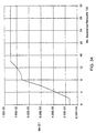
- Fig. 9 is a graph of the magnitude of the simulated electrical impedance
- the impedance value Z was computed by simulating the application of a 1 ampere constant current between the centers of the planes, varying the frequency of the current, and determining the magnitude of the steady state voltage between the centers of the rectangular planes.
- the electrical impedance between the parallel conductive planes of Fig. 8 is nearly constant from 1 MHz to about 50 Mhz. and increases almost monotonically at frequencies above 50 MHz.
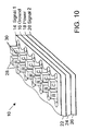
- Fig. 10 is a perspective view of a portion of interconnect apparatus 10 wherein impedance networks 12 are connected together to form a chain or "bar" of impedance networks 12.
- Each impedance network 12 is a spaced distance s from adjacent impedance networks 12.
- the bar of impedance networks 12 may extend along the entire length of an edge of the upper surface of interconnect apparatus 10.
- a bar of impedance networks 12 may extend across each of the four edges of the upper surface of a rectangular interconnect apparatus 10.
- Fig. 11 is a cross sectional view of a portion interconnecting apparatus 10 illustrating a second embodiment of impedance networks 12.
- each impedance network 12 includes a capacitance 50.
- a first via 52 connects power plane 18 to a first terminal of capacitance 50, and a second via 54 connects ground plane 16 to a second terminal of capacitance 50.
- Vias 52 and 54 may be, for example, plated-through holes formed using various well known techniques.
- An electrical resistance substantially equal to the value of resistance 28 is incorporated in series with capacitance 50.
- capacitance 50 may be selected such that it has an equivalent series resistance (ESR) substantially equal to the value of resistance 28.
- ESR equivalent series resistance
- vias 52 and 54 may be formed such that the sum of their resistances is substantially equal to the value of resistance 28.
- the resistances of vias 52 and 54 may be increased. for example, by reducing their cross sectional areas or by forming them from a material having a higher resistivity.
- Fig. 12 is a circuit diagram showing an equivalent electrical network 56 between power plane 18 and ground plane 16 provided by the impedance network 12 depicted in Fig. 11.
- Electrical network 56 includes an electrical resistance 58, an electrical inductance 60, and an electrical capacitance 62.
- the value of resistance 58 includes the ESR of capacitance 62 and the electrical resistances of vias 52 and 54.
- Inductance 60 includes the inductances of capacitor 50, via 52, and via 54.
- Capacitance 62 includes the value of capacitance 50.
- Fig. 13 is a cross sectional view of a portion of interconnecting apparatus 10 illustrating an alternate method of forming an electrical resistance and capacitance in series between two conductive planes separated by a dielectric layer.
- the conductive planes may be, for example, connected to different d.c. potentials as are a power plane and a ground plane.
- the multiple impedance networks 12 of Figs. 3-4 are replaced by a continuous (i.e., distributed) impedance network formed between regions of the conductive planes near peripheries.
- interconnecting apparatus 10 includes four electrically conductive planes: a first signal plane 64. a ground plane 66, a power plane 68. and a second signal plane 70.
- a planar electrically resistive layer 72 is between ground plane 66 and power plane 68 and in contact with ground plane 66.
- First signal plane 64 and ground plane 66 are separated by a first dielectric layer 74.
- Resistive layer 72 and power plane 68 are separated by a second dielectric layer 76.
- Power plane 68 and second signal plane 70 are separated by a third dielectric layer 78.
- a portion 80 around a region near the periphery of planar dielectric layer 76 has a higher relative dielectric constant than the relative dielectric constant of the remainder of dielectric layer 76.
- Portion 80 of dielectric layer 76 provides an electrical capacitance between power plane 68 and resistive layer 72.
- Resistive layer 72 provides a resistance between dielectric layer 76 and ground plane 66.
- the combination of portion 80 of dielectric layer 76 and resistive layer 72 between power plane 68 and ground plane 66 forms an electrical capacitance and an electrical resistance in series between power plane 68 and ground plane 66.
- the distributed impedance afforded by the series combination of the electrical capacitance and an electrical resistance is used to stabilize the electrical impedance between power plane 68 and ground plane 66.
- Resistive layer 72 may include, for example, electrically conductive particulates (e.g., silver, copper, or nickel) suspended in a non-conductive binder (e.g., epoxy resin, urethane. or polyester).
- the resistivity of the particulate-binder combination may be varied by changing the number of conductive particulates per unit volume of the particulate-binder combination. Increasing the number of suspended conductive particulates per unit volume of the particulate-binder combination decreases the resistivity of the particulate-binder combination. Decreasing the number of suspended conductive particulates per unit volume of the particulate-binder combination increases the resistivity of the particulate-binder combination.
- Resistive layer 72 is formed such that the electrical resistance between portion 80 of dielectric layer 76 and ground plane 66 along each edge of interconnect apparatus 10 is substantially equal to the characteristic impedance between power plane 68 and ground plane 66.
- the characteristic impedance " Zo " of the structure is calculated as: Accordingly, the electrical resistance between portion 80 of dielectric layer 76 and ground plane 66 along each edge of the structure is substantially equal to 0.070 ⁇ .
- planar resistive layer 72 may alternately be positioned between second dielectric layer 76 and power plane 68, and in contact with power plane 68.
- a first and second resistive layers may be positioned between ground plane 66 and power plane 68.
- the first resistive layer may be located between second dielectric layer 76 and ground plane 66, and in contact with ground plane 66.
- the second resistive may be located between second dielectric layer 76 and power plane 68, and in contact with power plane 68.
- the dielectric constant of portion 80 of dielectric layer 76 may be increased by suspending particulates of a substance having a relatively high dielectric constant (e.g., titanium dioxide or barium titanate) within a dielectric binder material (e.g., epoxy resin, polytetrafluoroethylene, or polystyrene).
- the dielectric constant of the particulate-binder combination may be varied by changing the number of particulates per unit volume of the particulate-binder combination. Increasing the number of suspended particulates per unit volume of the particulate-binder combination increases the dielectric constant of the particulate-binder combination. Decreasing the number of suspended particulates per unit volume of the particulate-binder combination decreases the dielectric constant of the particulate-binder combination.
- Portion 80 of dielectric layer 76 is preferably formed such that the capacitance per unit length C l provided by portion 80 between power plane 68 and ground plane 66 along each outer edge of rectangular interconnect apparatus 10 is given by: C 1 > 1 2 ⁇ ⁇ R 1 ⁇ ⁇ res where R l the resistance per unit length provided by resistive layer 72 and ⁇ res is the lowest resonant frequency of the structure including power plane 68, ground plane 66, and dielectric layer 76.
- Fig. 14 is a circuit diagram showing an equivalent electrical network 82 between power plane 68 and ground plane 66 provided by portion 80 of dielectric layer 76 and resistive layer 72 as depicted in Fig. 13.
- Electrical network 82 includes an electrical resistance 84 and an electrical capacitance 86.
- the value of resistance 84 includes the resistance of resistive layer 72 offered between portion 80 of dielectric layer 76 and ground plane 66.
- Capacitance 86 includes the value of the capacitance offered by portion 80 of dielectric layer 76. The value and effects of any inductance in series with resistance 84 and capacitance 86 are believed negligible in the embodiment of Fig. 13.
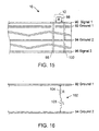
- Fig. 15 is a cross sectional view of a portion interconnecting apparatus 10 illustrating another alternate embodiment of impedance networks 12.
- impedance networks 12 are connected between a pair of planar conductors separated by at least one dielectric layer and connected to the same d.c. potential.
- the planar conductors may be. for example, two different ground planes.
- Each impedance network 12 includes an electrical resistance 88. The value of resistance 88 is determined in the same manner as described above for resistance 28.
- interconnecting apparatus 10 includes four electrically conductive planes: a first signal plane 90, a first ground plane 92, a second ground plane 94, and a second signal plane 96.
- Fig. 16 is a circuit diagram showing an equivalent electrical network 102 between first ground plane 92 and second ground plane 94 provided by the impedance network 12 depicted in Fig. 15.
- Electrical network 102 includes an electrical resistance 104 and an electrical inductance 106.
- the value of resistance 104 is substantially the sum of resistance 88 and the electrical resistances of vias 98 and 100.
- Inductance 106 is substantially the electrical inductances of vias 98 and 100.
- FIG. 17 is a perspective view of a structure 108 similar to structure 48 of Fig. 8.
- Structure 108 includes a pair of 8 in. x 8 in. square conductive plates separated by a dielectric layer (e.g., fiberglass-epoxy composite). Each conductive plate is made of copper and is 0.0014 in. thick.
- the dielectric layer separating the planes has a relative dielectric constant of 4.7 and a thickness or height h of 0.002 in.
- Multiple impedance networks 110 are connected between the plates about a region near a periphery of structure 108 as shown in Fig. 17. Adjacent impedance networks 110 are separated by a spaced distance s of 1.0 in.
- Structure 108 was modeled as a two-dimensional network (i.e., grid) of transmission line segments as described above.
- the grid included two orthogonal sets of parallel lines with spacings s superimposed upon one another.
- the two orthogonal sets of parallel lines intersected at nodes, and transmission line segments were connected between the nodes along the parallel lines.
- Each square s -by- s unit cell included four transmission line segments, one along each side of the unit cell.
- Transmission line segments in parallel were replaced by a single transmission line segment having half the characteristic impedance of the parallel segments.
- transmission line segments along outer edges of structure 108 had characteristic impedances twice those of transmission line segments between adjacent unit cells.
- the resulting grid had 81 nodes connected by transmission line segments.
- the electrical impedances of the all 81 grid nodes of the structure 108 model were simulated over a frequency range from 10 MHz to 1.000 MHz (i.e., 1 GHz). Between each set of simulations. the value of the electrical resistance of each impedance network 110 was varied. A normalized value the electrical resistance of each impedance network 110 was calculated by dividing the actual resistance value by the nominal value. The normalized value of the electrical resistance of each impedance network 110 was varied over the range between 0.01 and 1,000.
- the lowest value of the magnitudes of the impedances of the 81 grid nodes of the structure 108 model was determined.
- the lowest impedance magnitude value over the entire range of simulation frequencies.
- Min the lowest impedance magnitude value over the entire range of simulation frequencies.
- Min the lowest impedance magnitude value over the entire range of simulation frequencies.
- Min the lowest impedance magnitude value over the entire range of simulation frequencies.
- Min the Min
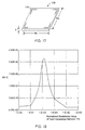
- Fig. 18 is a graph of the Min
- Fig. 18 shows that impedance networks 110 are effective in stabilizing the impedance of structure 108 over a wide range of normalized resistance values. Specifically, impedance networks 110 having normalized resistance values ranging from about 0.1 to approximately 100 are effective in stabilizing the impedance of structure 108. While impedance networks 110 having normalized resistance values of about 1.0 have the greatest stabilizing effect, normalized resistance values ranging from about 0.2 to approximately 10 are highly effective in stabilizing the impedance of structure 108.
- Fig. 19 is a top plan view of a grid 112 overlayed upon and covering an exemplary non-rectangular structure 114.
- Structure 114 includes two circular conductive plates arranged in parallel and separated by a dielectric layer.
- the two circular conductive plates may, for example. have diameters of 10 in., and the dielectric layer may have a thickness or height h of 0.002 in. and a relative dielectric constant of 4.7.
- Signals conveyed within structure 144 may have transition times of I nanosecond, leading to a highest frequency fm in a frequency range of interest of about 318 MHz.
- spacing distance s may be selected according to: s ⁇ c 10 ⁇ m ⁇ r where c is the speed of light, ⁇ m is a maximum frequency of a frequency range of interest. and ⁇ r is the relative dielectric constant of the dielectric layer.
- a highest frequency fm of 318 MHz and a relative dielectric constant of 4.7 leads to maximum spacings s of about 4.3 cm (approximately 1.7 in.).
- Spacings s may be selected to be, for example, 1.0 inch.
- the grid may then be generated using spacing distance s .
- the grid includes two orthogonal sets of parallel lines superimposed upon one another. The parallel lines within each set are separated by spacing distance s , and the grid is dimensioned such that it completely covers the structure when overlayed upon the structure.
- the grid may be generated by selecting orthogonal first and second dimensions of the structure. The first and second dimensions are preferably selected such that the product of the first and second dimensions is minimized. Corresponding first and second dimensions of the grid may then be sized such that they are greater than or equal to the respective first and second dimensions of the structure. As the parallel lines of the grid are separated by spacing distance s , the first and second dimensions of the grid are integer multiples of spacing distance s .
- dimensions w1 and w2 of grid 112 may be selected to be 10 in., the same as the diameters of the conductive circular plates of structure 114. As shown in Fig. 19, grid 112 may be overlayed upon structure 114 such that it completely covers structure 114. It is noted that other values of spacings s may require that dimensions w1 and w2 of grid 112 exceed the corresponding dimensions of structure 114 in order to allow grid 112 to completely cover structure 114 when overlayed upon structure 114. In general, it is desirable that the dimensions of grid 112 be the smallest possible which allow grid 112 to completely cover structure 114 when overlayed upon structure 114. In this case, the product of the orthogonal dimensions w1 and w2 of grid 112 will be minimized.
- the locations of the impedance networks to be dispersed about the periphery of structure 114 may be determined as shown in Fig. 19. Nodes nearest the periphery of structure 114, designated by "•" symbols in Fig. 19, are first selected as potential locations of the impedance networks. Potential locations not falling along the periphery of structure 114 are moved to an adjacent portion of the periphery of structure 114. The resulting locations of the impedance networks are designated by the "x" symbols in Fig. 19. The potential locations are preferably moved to adjacent portions of the periphery such that the distances between a given location and its nearest neighbors are substantially equal. In Fig. 19. this is accomplished by moving the potential locations along lines of grid 122 to adjacent portions of the periphery of structure 114.
- a potential location at node 116 is moved along line 118 of grid 122 to location 120 along the periphery of structure 114.
- the above example results in 28 impedance networks having resistance values of 0.348 ⁇ and dispersed about the periphery of structure 144 as shown in Fig. 19.
- the impedance networks are separated by an average distance of about 1.22 in.
- exemplary structure 114 in Fig. 19 is non-rectangular. It is noted that the general method described above may be used for determining electrical resistance values of. and locations for, impedance networks to be dispersed along a periphery of any structure including a pair of parallel planar conductors separated by a dielectric layer. whether the planar conductors be rectangular or non-rectangular.
- Figs. 20 and 21 will now be used to illustrate how tolerant the edge termination method is to resistance values and placements of impedance networks about the periphery of a structure.
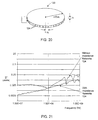
- Fig. 20 is a perspective view of structure 122 including two circular conductive plates arranged in parallel and separated by a dielectric layer. The two circular conductive plates have diameters of 10 in., and the dielectric layer has a thickness or height h of 0.002 in. and a relative dielectric constant of 4.7.
- Fig. 21 is a graph of the magnitude of the measured impedance
- the electrical impedance of the "unterminated" structure 122 without impedance networks 124 varies greatly at frequencies above about 50 MHz.
- the parallel conductive plates exhibit multiple electrical resonances at frequencies between about 300 MHz and 1 GHz, resulting in alternating high and low impedance values.
- the electrical impedance of the "edge terminated" structure 122 with impedance networks 124 rises monotonically from 10 MHz to about 500 Mhz, and the multiple electrical resonances present without impedance networks 124 between about 300 MHz and I GHz are damped considerably.
- the impedance of structure 122 is thus stabilized significantly by the additions of impedance networks 124. It is believed the edge terminated structure 122 with impedance networks 124 would radiate a substantially smaller amount of EMI than the unterminated structure 122 without impedance networks 124.
- Figs. 22-26 will now be used to show how the simulated effects of eliminating impedance networks along one or more sides of a rectangular structure impacts the beneficial impedance-stabilizing effects of edge termination.
- Fig. 22 is a top plan view of a structure 126 including a pair of 10 in. x 10 in. square conductive plates separated by a dielectric layer. Each conductive plate or sheet is made of copper and 0.0014 in. thick. The dielectric layer separating the planes has a relative dielectric constant of 4.7 and a thickness or height h of 0.002 in.
- Multiple impedance networks 128 are dispersed about a region near the periphery of structure 126 as shown in Fig. 22. The selected spacings s were 1.0 in.
- Figs. 23-25 show structure 126 with impedance networks 128 removed from one, two, and three sides respectively. In Figs. 23-25, impedance networks 128 removed from structure 126 are marked with an "x" symbol.
- Structure 126 was modeled as a two-dimensional network (i.e., grid) of transmission line segments as described above.
- the grid included two orthogonal sets of parallel lines with spacings s superimposed upon one another.
- the orthogonal sets of parallel lines intersected at nodes, and transmission line segments connected nodes along the parallel lines.
- the resulting grid had 121 nodes connected by transmission line segments.
Landscapes
- Physics & Mathematics (AREA)
- Electromagnetism (AREA)
- Engineering & Computer Science (AREA)
- Microelectronics & Electronic Packaging (AREA)
- Coupling Device And Connection With Printed Circuit (AREA)
- Details Of Connecting Devices For Male And Female Coupling (AREA)
- Internal Circuitry In Semiconductor Integrated Circuit Devices (AREA)
- Structure Of Printed Boards (AREA)
- Non-Reversible Transmitting Devices (AREA)
- Production Of Multi-Layered Print Wiring Board (AREA)
Claims (18)
- Verfahren zum Stabilisieren der elektrischen Impedanz einer im wesentlichen rechteckigen elektrischen Energieverteilungsstruktur mit:Bestimmen einer charakteristischen Impedanz Z0 der Struktur, wobeidie Struktur ein Paar paralleler ebener elektrischer Leiter aufweist, die durch eine dielektrische Schicht voneinander getrennt sind, undelektrisches Anschließen von n elektrischen Widerständen zwischen den ebenen Leitern entlang einer Seite der Struktur, wobei n ≥ 2, und wobei jeder der n elektrischen Widerstände einen Wert hat, der im wesentlichen gleich n x Z0 ist.
- Verfahren nach Anspruch 1, wobei die elektrischen Widerstände diskrete elektrische Widerstände sind, die entlang einer äußeren Kante an der Seite der Struktur verteilt sind.
- Verfahren nach Anspruch 1 oder 2, wobei die Struktur quadratisch ist und vier Seiten gleicher Länge w hat, und wobei die charakteristische Impedanz Z0 der Struktur gegeben ist durch:und wobei Z00 die Impedanz des freien Raumes ist, h der Abstand zwischen den ebenen elektrischen Leitem ist und εr die relative Dielektrizitätskonstante der dielektrischen Schicht ist.

- Verfahren nach einem der Ansprüche 1 bis 3, wobei der Anschluß so ausgeführt wird, daß zwischen den n elektrischen Widerständen ein einzelner seitlicher Zwischenabstand aufrechterhalten wird.
- Elektrische Verbindungseinrichtung mit:einem Paar paralleler elektrischer Leiter, die durch eine dielektrische Schicht voneinander getrennt sind,wobei jeder ebene elektrische Leiter im wesentlichen rechteckig ist und vier Seiten hat und wobei jeder elektrische Leiter einen äußeren Bereich in der Nähe der vier Seiten hat, und miteiner Mehrzahl von Impedanznetzwerken, die elektrisch zwischen die äußeren Bereiche der ebenen Leiter geschaltet sind, wobei jedes Impedanznetzwerk einen elektrischen Widerstand einschließt und wobei n der Impedanznetzwerke entlang einer Seite der elektrischen Verbindungsvorrichtung vorliegen und wobei n ≥ 2 und der elektrische Widerstand jedes der n Impedanznetzwerke einen Wert hat, der im wesentlichen dem n-fachen der charakteristischen Impedanz der ebenen elektrischen Leiter entspricht.
- Elektrische Verbindungsvorrichtung nach Anspruch 5, wobei jedes Impedanznetzwerk auf einer oberen Fläche der elektrischen Verbindungseinrichtung angeordnet ist und wobei ein Paar von Durchgängen verwendet wird, um jedes Impedanznetzwerk zwischen die äußeren Bereiche der ebenen elektrischen Leiter zu schalten bzw. zwischen diesen anzuschließen.
- Elektrische Verbindungsvorrichtung nach Anspruch 5 oder 6, wobei die Mehrzahl von Impedanznetzwerken durch einen vorbestimmten Zwischenabstand voneinander getrennt sind.
- Elektrische Verbindungsvorrichtung nach Anspruch 7, wobei n ≥ 2 und wobei die n Impedanznetzwerke durch einen einzigen seitlichen Zwischenabstand voneinander getrennt sind.
- Elektrische Verbindungsvorrichtung nach Anspruch 7 oder 8, wobei Signale in der elektrischen Verbindungsvorrichtung übertragen werden und wobei die Signale einen zugehörigen Frequenzbereich haben und der Zwischenabstand zwischen den Impedanznetzwerken gleich einem Bruchteil der Wellenlänge der höchsten Frequenz in diesem Frequenzbereich ist.
- Elektrische Verbindungsvorrichtung nach Anspruch 9, wobei die elektrische Verbindungsvorrichtung weiterhin eine Signalschicht aufweist, die von den Paaren paralleler ebener elektrischer Leiter getrennt ist, und wobei die Signalschicht Bahnen zum Transportieren der Signale umfaßt.
- Elektrische Verbindungsvorrichtung nach Anspruch 9 oder 10, wobei der Zwischenabstand zwischen den Impedanznetzwerken kleiner oder gleich einem Zehntel der Wellenlänge der höchsten Frequenz in dem Frequenzbereich ist.
- Elektrische Verbindungsvorrichtung nach einem der Ansprüche 5 bis 11, wobei n Impedanznetzwerke miteinander verbunden sind, um eine Kette von Impedanznetzwerken zu bilden.
- Elektrische Verbindungsvorrichtung nach einem der Ansprüche 5 bis 12, wobei jedes Impedanznetzwerk weiterhin einen elektrischen Kondensator in Reihe mit dem elektrischen Widerstand aufweist.
- Elektrische Verbindungsvorrichtung nach einem der Ansprüche 5 bis 13, wobei die elektrische Verbindungseinrichtung eine gedruckte Schaltkreisplatine ist.
- Elektrische Verbindungsvorrichtung nach einem der Ansprüche 5 bis 14, wobei die dielektrische Schicht ein Fiberglas-Epoxidharzverbundteil ist.
- Elektrische Verbindungsvorrichtung nach einem der Ansprüche 5 bis 15, wobei jeder der ebenen elektrischen Leiter über zumindest einen Teil der elektrischen Verbindungsvorrichtung hinweg kontinuierlich verläuft.
- Elektrische Verbindungsvorrichtung nach einem der Ansprüche 5 bis 16, wobei die Paare ebener elektrischer Leiter für die Verbindung mit unterschiedlichen Energiezufuhrpotentialen ausgelegt sind.
- Elektrische Verbindungsvorrichtung nach einem der Ansprüche 5 bis 17, wobei das Paar ebener elektrischer Leiter für das Verbinden mit demselben Energiezufuhrpotential ausgelegt ist.
Applications Claiming Priority (5)
| Application Number | Priority Date | Filing Date | Title |
|---|---|---|---|
| US81372 | 1998-05-19 | ||
| US09/081,372 US6104258A (en) | 1998-05-19 | 1998-05-19 | System and method for edge termination of parallel conductive planes in an electrical interconnecting apparatus |
| US246654 | 1999-02-08 | ||
| US09/246,654 US6215373B1 (en) | 1998-05-19 | 1999-02-08 | Method for edge termination of parallel conductive planes including estimating the characteristic impedance of the structure |
| PCT/US1999/010937 WO1999060699A1 (en) | 1998-05-19 | 1999-05-18 | System and method for edge termination of parallel conductive planes in an electrical interconnecting apparatus |
Publications (2)
| Publication Number | Publication Date |
|---|---|
| EP1078452A1 EP1078452A1 (de) | 2001-02-28 |
| EP1078452B1 true EP1078452B1 (de) | 2001-11-28 |
Family
ID=26765513
Family Applications (1)
| Application Number | Title | Priority Date | Filing Date |
|---|---|---|---|
| EP99923182A Expired - Lifetime EP1078452B1 (de) | 1998-05-19 | 1999-05-18 | Verfahren und system zum randabschluss von parallelen leitenden oberflächen in einer elektrischen verbindungsvorrichtung |
Country Status (7)
| Country | Link |
|---|---|
| US (1) | US6215373B1 (de) |
| EP (1) | EP1078452B1 (de) |
| JP (1) | JP2003517740A (de) |
| AT (1) | ATE209831T1 (de) |
| AU (1) | AU4000999A (de) |
| DE (1) | DE69900505T2 (de) |
| WO (1) | WO1999060699A1 (de) |
Families Citing this family (34)
| Publication number | Priority date | Publication date | Assignee | Title |
|---|---|---|---|---|
| US9054094B2 (en) | 1997-04-08 | 2015-06-09 | X2Y Attenuators, Llc | Energy conditioning circuit arrangement for integrated circuit |
| US7321485B2 (en) | 1997-04-08 | 2008-01-22 | X2Y Attenuators, Llc | Arrangement for energy conditioning |
| US7336468B2 (en) | 1997-04-08 | 2008-02-26 | X2Y Attenuators, Llc | Arrangement for energy conditioning |
| US7301748B2 (en) | 1997-04-08 | 2007-11-27 | Anthony Anthony A | Universal energy conditioning interposer with circuit architecture |
| JP3501674B2 (ja) * | 1999-04-21 | 2004-03-02 | 日本電気株式会社 | プリント回路基板特性評価装置、プリント回路基板特性評価方法、及び記憶媒体 |
| US6441313B1 (en) * | 1999-11-23 | 2002-08-27 | Sun Microsystems, Inc. | Printed circuit board employing lossy power distribution network to reduce power plane resonances |
| US6775122B1 (en) * | 1999-12-28 | 2004-08-10 | Intel Corporation | Circuit board with added impedance |
| US6509640B1 (en) * | 2000-09-29 | 2003-01-21 | Intel Corporation | Integral capacitor using embedded enclosure for effective electromagnetic radiation reduction |
| US6525622B1 (en) * | 2000-11-17 | 2003-02-25 | Sun Microsystems, Inc. | Adding electrical resistance in series with bypass capacitors to achieve a desired value of electrical impedance between conducts of an electrical power distribution structure |
| US6901343B2 (en) * | 2001-01-10 | 2005-05-31 | Matsushita Electric Industrial Co., Ltd. | Multilayer board in which wiring of signal line that requires tamper-resistance is covered by component or foil, design apparatus, method, and program for the multilayer board, and medium recording the program |
| US6704669B2 (en) * | 2001-04-25 | 2004-03-09 | International Business Machines Corporation | Method for determining voltage, current, and/or power distributions in a resistive structure using a rectangular grid algorithm modified for non-rectangular holes and contacts |
| US6727780B2 (en) | 2001-10-24 | 2004-04-27 | Sun Microsystems, Inc. | Adding electrical resistance in series with bypass capacitors using annular resistors |
| US6608257B1 (en) | 2001-12-12 | 2003-08-19 | Sun Microsystems, Inc. | Direct plane attachment for capacitors |
| DE10305520A1 (de) * | 2003-02-11 | 2004-08-19 | Robert Bosch Gmbh | Vorrichtung und Verfahren zur Dämpfung von Hohlraumresonanzen in einer mehrschichtigen Trägereinrichtung |
| US7010768B2 (en) * | 2003-06-17 | 2006-03-07 | International Business Machines Corporation | Transmission line bounding models |
| US6963204B2 (en) * | 2004-04-06 | 2005-11-08 | International Business Machines Corporation | Method to include delta-I noise on chip using lossy transmission line representation for the power mesh |
| US7376408B2 (en) * | 2004-08-10 | 2008-05-20 | Sony Ericsson Mobile Communications Ab | Reduction of near field electro-magnetic scattering using high impedance metallization terminations |
| CN1764346B (zh) * | 2004-10-19 | 2012-05-30 | 辉达公司 | 一种可以降低一印刷电路板的电源阻抗的方法 |
| WO2006093831A2 (en) | 2005-03-01 | 2006-09-08 | X2Y Attenuators, Llc | Energy conditioner with tied through electrodes |
| JP2008537843A (ja) | 2005-03-01 | 2008-09-25 | エックストゥーワイ アテニュエイターズ,エルエルシー | 内部で重なり合った調整器 |
| US20070003088A1 (en) * | 2005-06-27 | 2007-01-04 | Nokia Corporation | Hearing aid compatible mobile phone and method |
| US20070152771A1 (en) * | 2006-01-05 | 2007-07-05 | Lei Shan | Apparatus and method of via-stub resonance extinction |
| WO2007103965A1 (en) | 2006-03-07 | 2007-09-13 | X2Y Attenuators, Llc | Energy conditioner structures |
| US20070279882A1 (en) * | 2006-06-06 | 2007-12-06 | Samtec, Inc. | Power distribution system for integrated circuits |
| US7886431B2 (en) * | 2006-06-06 | 2011-02-15 | Teraspeed Consulting Group Llc | Power distribution system for integrated circuits |
| US7773390B2 (en) * | 2006-06-06 | 2010-08-10 | Teraspeed Consulting Group Llc | Power distribution system for integrated circuits |
| US20080068818A1 (en) * | 2006-09-19 | 2008-03-20 | Jinwoo Choi | Method and apparatus for providing ultra-wide band noise isolation in printed circuit boards |
| US8059423B2 (en) * | 2007-02-06 | 2011-11-15 | Sanmina-Sci Corporation | Enhanced localized distributive capacitance for circuit boards |
| JP5229945B2 (ja) * | 2008-09-09 | 2013-07-03 | 太陽誘電株式会社 | フィルタ、デュープレクサ、および通信装置 |
| US8923528B2 (en) | 2010-08-30 | 2014-12-30 | Microsoft Corporation | Hearing aid-compatible apparatus for wireless communication devices |
| US8952503B2 (en) | 2013-01-29 | 2015-02-10 | International Business Machines Corporation | Organic module EMI shielding structures and methods |
| US20140326489A1 (en) * | 2013-05-03 | 2014-11-06 | Dell Products L.P. | Systems and methods for decreasing stub resonance of plating for circuit boards |
| CN104854792B (zh) * | 2013-10-17 | 2018-11-06 | 株式会社村田制作所 | 高频电路 |
| US20160183386A1 (en) * | 2014-12-19 | 2016-06-23 | Qualcomm Incorporated | Techniques for controlling equivalent series resistance of a capacitor |
Citations (2)
| Publication number | Priority date | Publication date | Assignee | Title |
|---|---|---|---|---|
| US4626889A (en) * | 1983-12-23 | 1986-12-02 | Hitachi, Ltd. | Stacked differentially driven transmission line on integrated circuit |
| US5708400A (en) * | 1996-10-30 | 1998-01-13 | Hewlett-Packard Company | AC coupled termination of a printed circuit board power plane in its characteristic impedance |
Family Cites Families (4)
| Publication number | Priority date | Publication date | Assignee | Title |
|---|---|---|---|---|
| US4371746A (en) | 1978-01-05 | 1983-02-01 | Peptek, Incorporated | Edge terminations for impedance planes |
| US5114912A (en) | 1991-05-13 | 1992-05-19 | The United States Of America As Represented By The Secretary Of Commerce | Two-dimensional, Josephson-array, voltage-tunable, high-frequency oscillator |
| US5266036A (en) | 1992-06-02 | 1993-11-30 | Hewlett-Packard Company | Reduction of radio frequency emissions through terminating geometrically induced transmission lines in computer products |
| US5818315A (en) * | 1996-12-31 | 1998-10-06 | Lucent Technologies Inc. | Signal trace impedance control using a grid-like ground plane |
-
1999
- 1999-02-08 US US09/246,654 patent/US6215373B1/en not_active Expired - Lifetime
- 1999-05-18 AT AT99923182T patent/ATE209831T1/de not_active IP Right Cessation
- 1999-05-18 EP EP99923182A patent/EP1078452B1/de not_active Expired - Lifetime
- 1999-05-18 WO PCT/US1999/010937 patent/WO1999060699A1/en not_active Ceased
- 1999-05-18 JP JP2000550206A patent/JP2003517740A/ja active Pending
- 1999-05-18 AU AU40009/99A patent/AU4000999A/en not_active Abandoned
- 1999-05-18 DE DE69900505T patent/DE69900505T2/de not_active Expired - Fee Related
Patent Citations (2)
| Publication number | Priority date | Publication date | Assignee | Title |
|---|---|---|---|---|
| US4626889A (en) * | 1983-12-23 | 1986-12-02 | Hitachi, Ltd. | Stacked differentially driven transmission line on integrated circuit |
| US5708400A (en) * | 1996-10-30 | 1998-01-13 | Hewlett-Packard Company | AC coupled termination of a printed circuit board power plane in its characteristic impedance |
Also Published As
| Publication number | Publication date |
|---|---|
| DE69900505T2 (de) | 2002-07-18 |
| JP2003517740A (ja) | 2003-05-27 |
| ATE209831T1 (de) | 2001-12-15 |
| WO1999060699A1 (en) | 1999-11-25 |
| AU4000999A (en) | 1999-12-06 |
| DE69900505D1 (de) | 2002-01-10 |
| US6215373B1 (en) | 2001-04-10 |
| EP1078452A1 (de) | 2001-02-28 |
Similar Documents
| Publication | Publication Date | Title |
|---|---|---|
| US6215373B1 (en) | Method for edge termination of parallel conductive planes including estimating the characteristic impedance of the structure | |
| US6104258A (en) | System and method for edge termination of parallel conductive planes in an electrical interconnecting apparatus | |
| US6441313B1 (en) | Printed circuit board employing lossy power distribution network to reduce power plane resonances | |
| US6532439B2 (en) | Method for determining the desired decoupling components for power distribution systems | |
| EP1088345B1 (de) | System und verfahren zur bestimmung der gewünschten entkupplungselemente für ein energieverteilungssystem unter verwendung eines rechnersystems | |
| US6215372B1 (en) | Method and apparatus for reducing electrical resonances in power and noise propagation in power distribution circuits employing plane conductors | |
| US6674338B2 (en) | Adding electrical resistance in series with bypass capacitors to achieve a desired value of electrical impedance between conductors of an electrical power distribution structure | |
| US8595924B2 (en) | Method of electromagnetic noise suppression devices using hybrid electromagnetic bandgap structures | |
| US6571184B2 (en) | System and method for determining the decoupling capacitors for power distribution systems with a frequency-dependent target impedance | |
| KR19980064807A (ko) | 격자형 접지판을 이용한 신호 트레이스 임피던스 제어 | |
| WO2001017111A9 (en) | A system and method for analyzing simultaneous switching noise | |
| EP1295516B1 (de) | Überbrückungskondensator-verfahren zum erreichen eines gewünschten elektrischen impedanzwerts zwischen parallelen planaren leitern einer elektrischen stromverteilungsstruktur, und zugehörige elektrische stromverteilungsstrukturen | |
| Wu et al. | Delaunay–Voronoi modeling of power-ground planes with source port correction | |
| US6727780B2 (en) | Adding electrical resistance in series with bypass capacitors using annular resistors | |
| WO2004051789A1 (en) | A circuit that taps a differential signal | |
| US6559733B2 (en) | Reducing effects of electrical impedance | |
| HK1034601B (en) | System and method for determining the desired decoupling components for power distribution systems using a computer system |
Legal Events
| Date | Code | Title | Description |
|---|---|---|---|
| PUAI | Public reference made under article 153(3) epc to a published international application that has entered the european phase |
Free format text: ORIGINAL CODE: 0009012 |
|
| 17P | Request for examination filed |
Effective date: 20001106 |
|
| AK | Designated contracting states |
Kind code of ref document: A1 Designated state(s): AT BE CH CY DE DK ES FI FR GB GR IE IT LI LU MC NL PT SE |
|
| GRAG | Despatch of communication of intention to grant |
Free format text: ORIGINAL CODE: EPIDOS AGRA |
|
| 17Q | First examination report despatched |
Effective date: 20010319 |
|
| GRAG | Despatch of communication of intention to grant |
Free format text: ORIGINAL CODE: EPIDOS AGRA |
|
| GRAH | Despatch of communication of intention to grant a patent |
Free format text: ORIGINAL CODE: EPIDOS IGRA |
|
| GRAH | Despatch of communication of intention to grant a patent |
Free format text: ORIGINAL CODE: EPIDOS IGRA |
|
| GRAA | (expected) grant |
Free format text: ORIGINAL CODE: 0009210 |
|
| AK | Designated contracting states |
Kind code of ref document: B1 Designated state(s): AT BE CH CY DE DK ES FI FR GB GR IE IT LI LU MC NL PT SE |
|
| PG25 | Lapsed in a contracting state [announced via postgrant information from national office to epo] |
Ref country code: NL Free format text: LAPSE BECAUSE OF FAILURE TO SUBMIT A TRANSLATION OF THE DESCRIPTION OR TO PAY THE FEE WITHIN THE PRESCRIBED TIME-LIMIT Effective date: 20011128 Ref country code: LI Free format text: LAPSE BECAUSE OF FAILURE TO SUBMIT A TRANSLATION OF THE DESCRIPTION OR TO PAY THE FEE WITHIN THE PRESCRIBED TIME-LIMIT Effective date: 20011128 Ref country code: IT Free format text: LAPSE BECAUSE OF FAILURE TO SUBMIT A TRANSLATION OF THE DESCRIPTION OR TO PAY THE FEE WITHIN THE PRESCRIBED TIME-LIMIT;WARNING: LAPSES OF ITALIAN PATENTS WITH EFFECTIVE DATE BEFORE 2007 MAY HAVE OCCURRED AT ANY TIME BEFORE 2007. THE CORRECT EFFECTIVE DATE MAY BE DIFFERENT FROM THE ONE RECORDED. Effective date: 20011128 Ref country code: GR Free format text: LAPSE BECAUSE OF FAILURE TO SUBMIT A TRANSLATION OF THE DESCRIPTION OR TO PAY THE FEE WITHIN THE PRESCRIBED TIME-LIMIT Effective date: 20011128 Ref country code: FI Free format text: LAPSE BECAUSE OF FAILURE TO SUBMIT A TRANSLATION OF THE DESCRIPTION OR TO PAY THE FEE WITHIN THE PRESCRIBED TIME-LIMIT Effective date: 20011128 Ref country code: CH Free format text: LAPSE BECAUSE OF FAILURE TO SUBMIT A TRANSLATION OF THE DESCRIPTION OR TO PAY THE FEE WITHIN THE PRESCRIBED TIME-LIMIT Effective date: 20011128 Ref country code: BE Free format text: LAPSE BECAUSE OF FAILURE TO SUBMIT A TRANSLATION OF THE DESCRIPTION OR TO PAY THE FEE WITHIN THE PRESCRIBED TIME-LIMIT Effective date: 20011128 Ref country code: AT Free format text: LAPSE BECAUSE OF FAILURE TO SUBMIT A TRANSLATION OF THE DESCRIPTION OR TO PAY THE FEE WITHIN THE PRESCRIBED TIME-LIMIT Effective date: 20011128 |
|
| REF | Corresponds to: |
Ref document number: 209831 Country of ref document: AT Date of ref document: 20011215 Kind code of ref document: T |
|
| REG | Reference to a national code |
Ref country code: CH Ref legal event code: EP |
|
| REG | Reference to a national code |
Ref country code: IE Ref legal event code: FG4D |
|
| REG | Reference to a national code |
Ref country code: GB Ref legal event code: IF02 |
|
| REF | Corresponds to: |
Ref document number: 69900505 Country of ref document: DE Date of ref document: 20020110 |
|
| PG25 | Lapsed in a contracting state [announced via postgrant information from national office to epo] |
Ref country code: SE Free format text: LAPSE BECAUSE OF FAILURE TO SUBMIT A TRANSLATION OF THE DESCRIPTION OR TO PAY THE FEE WITHIN THE PRESCRIBED TIME-LIMIT Effective date: 20020228 Ref country code: PT Free format text: LAPSE BECAUSE OF FAILURE TO SUBMIT A TRANSLATION OF THE DESCRIPTION OR TO PAY THE FEE WITHIN THE PRESCRIBED TIME-LIMIT Effective date: 20020228 Ref country code: DK Free format text: LAPSE BECAUSE OF FAILURE TO SUBMIT A TRANSLATION OF THE DESCRIPTION OR TO PAY THE FEE WITHIN THE PRESCRIBED TIME-LIMIT Effective date: 20020228 |
|
| NLV1 | Nl: lapsed or annulled due to failure to fulfill the requirements of art. 29p and 29m of the patents act | ||
| ET | Fr: translation filed | ||
| PGFP | Annual fee paid to national office [announced via postgrant information from national office to epo] |
Ref country code: IE Payment date: 20020529 Year of fee payment: 4 |
|
| PG25 | Lapsed in a contracting state [announced via postgrant information from national office to epo] |
Ref country code: ES Free format text: LAPSE BECAUSE OF FAILURE TO SUBMIT A TRANSLATION OF THE DESCRIPTION OR TO PAY THE FEE WITHIN THE PRESCRIBED TIME-LIMIT Effective date: 20020530 |
|
| PG25 | Lapsed in a contracting state [announced via postgrant information from national office to epo] |
Ref country code: CY Free format text: LAPSE BECAUSE OF FAILURE TO SUBMIT A TRANSLATION OF THE DESCRIPTION OR TO PAY THE FEE WITHIN THE PRESCRIBED TIME-LIMIT Effective date: 20020531 |
|
| PGFP | Annual fee paid to national office [announced via postgrant information from national office to epo] |
Ref country code: MC Payment date: 20020531 Year of fee payment: 4 |
|
| PGFP | Annual fee paid to national office [announced via postgrant information from national office to epo] |
Ref country code: LU Payment date: 20020605 Year of fee payment: 4 |
|
| REG | Reference to a national code |
Ref country code: CH Ref legal event code: PL |
|
| PLBE | No opposition filed within time limit |
Free format text: ORIGINAL CODE: 0009261 |
|
| STAA | Information on the status of an ep patent application or granted ep patent |
Free format text: STATUS: NO OPPOSITION FILED WITHIN TIME LIMIT |
|
| 26N | No opposition filed | ||
| PG25 | Lapsed in a contracting state [announced via postgrant information from national office to epo] |
Ref country code: LU Free format text: LAPSE BECAUSE OF NON-PAYMENT OF DUE FEES Effective date: 20030518 |
|
| PG25 | Lapsed in a contracting state [announced via postgrant information from national office to epo] |
Ref country code: IE Free format text: LAPSE BECAUSE OF NON-PAYMENT OF DUE FEES Effective date: 20030519 |
|
| PGFP | Annual fee paid to national office [announced via postgrant information from national office to epo] |
Ref country code: FR Payment date: 20030528 Year of fee payment: 5 |
|
| PG25 | Lapsed in a contracting state [announced via postgrant information from national office to epo] |
Ref country code: MC Free format text: LAPSE BECAUSE OF NON-PAYMENT OF DUE FEES Effective date: 20030531 |
|
| PGFP | Annual fee paid to national office [announced via postgrant information from national office to epo] |
Ref country code: GB Payment date: 20030611 Year of fee payment: 5 |
|
| PGFP | Annual fee paid to national office [announced via postgrant information from national office to epo] |
Ref country code: DE Payment date: 20030724 Year of fee payment: 5 |
|
| REG | Reference to a national code |
Ref country code: IE Ref legal event code: MM4A |
|
| PG25 | Lapsed in a contracting state [announced via postgrant information from national office to epo] |
Ref country code: GB Free format text: LAPSE BECAUSE OF NON-PAYMENT OF DUE FEES Effective date: 20040518 |
|
| PG25 | Lapsed in a contracting state [announced via postgrant information from national office to epo] |
Ref country code: DE Free format text: LAPSE BECAUSE OF NON-PAYMENT OF DUE FEES Effective date: 20041201 |
|
| GBPC | Gb: european patent ceased through non-payment of renewal fee |
Effective date: 20040518 |
|
| PG25 | Lapsed in a contracting state [announced via postgrant information from national office to epo] |
Ref country code: FR Free format text: LAPSE BECAUSE OF NON-PAYMENT OF DUE FEES Effective date: 20050131 |
|
| REG | Reference to a national code |
Ref country code: FR Ref legal event code: ST |