EP1079512A1 - Dispositif d'oscillateur à deux bandes - Google Patents
Dispositif d'oscillateur à deux bandes Download PDFInfo
- Publication number
- EP1079512A1 EP1079512A1 EP00306529A EP00306529A EP1079512A1 EP 1079512 A1 EP1079512 A1 EP 1079512A1 EP 00306529 A EP00306529 A EP 00306529A EP 00306529 A EP00306529 A EP 00306529A EP 1079512 A1 EP1079512 A1 EP 1079512A1
- Authority
- EP
- European Patent Office
- Prior art keywords
- oscillator
- frequency band
- amplifier
- oscillation signal
- oscillation
- Prior art date
- Legal status (The legal status is an assumption and is not a legal conclusion. Google has not performed a legal analysis and makes no representation as to the accuracy of the status listed.)
- Granted
Links
- 230000010355 oscillation Effects 0.000 claims abstract description 146
- 230000008878 coupling Effects 0.000 claims abstract description 54
- 238000010168 coupling process Methods 0.000 claims abstract description 54
- 238000005859 coupling reaction Methods 0.000 claims abstract description 54
- 239000003990 capacitor Substances 0.000 claims description 61
- 238000010276 construction Methods 0.000 description 15
- 230000003321 amplification Effects 0.000 description 7
- 238000003199 nucleic acid amplification method Methods 0.000 description 7
- 230000000903 blocking effect Effects 0.000 description 5
- 238000010586 diagram Methods 0.000 description 5
- 230000004048 modification Effects 0.000 description 3
- 238000012986 modification Methods 0.000 description 3
- 230000003247 decreasing effect Effects 0.000 description 1
Images


Classifications
-
- H—ELECTRICITY
- H03—ELECTRONIC CIRCUITRY
- H03B—GENERATION OF OSCILLATIONS, DIRECTLY OR BY FREQUENCY-CHANGING, BY CIRCUITS EMPLOYING ACTIVE ELEMENTS WHICH OPERATE IN A NON-SWITCHING MANNER; GENERATION OF NOISE BY SUCH CIRCUITS
- H03B5/00—Generation of oscillations using amplifier with regenerative feedback from output to input
- H03B5/02—Details
- H03B5/04—Modifications of generator to compensate for variations in physical values, e.g. power supply, load, temperature
-
- H—ELECTRICITY
- H03—ELECTRONIC CIRCUITRY
- H03B—GENERATION OF OSCILLATIONS, DIRECTLY OR BY FREQUENCY-CHANGING, BY CIRCUITS EMPLOYING ACTIVE ELEMENTS WHICH OPERATE IN A NON-SWITCHING MANNER; GENERATION OF NOISE BY SUCH CIRCUITS
- H03B5/00—Generation of oscillations using amplifier with regenerative feedback from output to input
- H03B5/18—Generation of oscillations using amplifier with regenerative feedback from output to input with frequency-determining element comprising distributed inductance and capacitance
- H03B5/1841—Generation of oscillations using amplifier with regenerative feedback from output to input with frequency-determining element comprising distributed inductance and capacitance the frequency-determining element being a strip line resonator
- H03B5/1847—Generation of oscillations using amplifier with regenerative feedback from output to input with frequency-determining element comprising distributed inductance and capacitance the frequency-determining element being a strip line resonator the active element in the amplifier being a semiconductor device
-
- H—ELECTRICITY
- H03—ELECTRONIC CIRCUITRY
- H03B—GENERATION OF OSCILLATIONS, DIRECTLY OR BY FREQUENCY-CHANGING, BY CIRCUITS EMPLOYING ACTIVE ELEMENTS WHICH OPERATE IN A NON-SWITCHING MANNER; GENERATION OF NOISE BY SUCH CIRCUITS
- H03B5/00—Generation of oscillations using amplifier with regenerative feedback from output to input
- H03B5/08—Generation of oscillations using amplifier with regenerative feedback from output to input with frequency-determining element comprising lumped inductance and capacitance
- H03B5/12—Generation of oscillations using amplifier with regenerative feedback from output to input with frequency-determining element comprising lumped inductance and capacitance active element in amplifier being semiconductor device
- H03B5/1203—Generation of oscillations using amplifier with regenerative feedback from output to input with frequency-determining element comprising lumped inductance and capacitance active element in amplifier being semiconductor device the amplifier being a single transistor
-
- H—ELECTRICITY
- H03—ELECTRONIC CIRCUITRY
- H03B—GENERATION OF OSCILLATIONS, DIRECTLY OR BY FREQUENCY-CHANGING, BY CIRCUITS EMPLOYING ACTIVE ELEMENTS WHICH OPERATE IN A NON-SWITCHING MANNER; GENERATION OF NOISE BY SUCH CIRCUITS
- H03B5/00—Generation of oscillations using amplifier with regenerative feedback from output to input
- H03B5/08—Generation of oscillations using amplifier with regenerative feedback from output to input with frequency-determining element comprising lumped inductance and capacitance
- H03B5/12—Generation of oscillations using amplifier with regenerative feedback from output to input with frequency-determining element comprising lumped inductance and capacitance active element in amplifier being semiconductor device
- H03B5/1231—Generation of oscillations using amplifier with regenerative feedback from output to input with frequency-determining element comprising lumped inductance and capacitance active element in amplifier being semiconductor device the amplifier comprising one or more bipolar transistors
-
- H—ELECTRICITY
- H03—ELECTRONIC CIRCUITRY
- H03B—GENERATION OF OSCILLATIONS, DIRECTLY OR BY FREQUENCY-CHANGING, BY CIRCUITS EMPLOYING ACTIVE ELEMENTS WHICH OPERATE IN A NON-SWITCHING MANNER; GENERATION OF NOISE BY SUCH CIRCUITS
- H03B5/00—Generation of oscillations using amplifier with regenerative feedback from output to input
- H03B5/08—Generation of oscillations using amplifier with regenerative feedback from output to input with frequency-determining element comprising lumped inductance and capacitance
- H03B5/12—Generation of oscillations using amplifier with regenerative feedback from output to input with frequency-determining element comprising lumped inductance and capacitance active element in amplifier being semiconductor device
- H03B5/1237—Generation of oscillations using amplifier with regenerative feedback from output to input with frequency-determining element comprising lumped inductance and capacitance active element in amplifier being semiconductor device comprising means for varying the frequency of the generator
- H03B5/124—Generation of oscillations using amplifier with regenerative feedback from output to input with frequency-determining element comprising lumped inductance and capacitance active element in amplifier being semiconductor device comprising means for varying the frequency of the generator the means comprising a voltage dependent capacitance
- H03B5/1243—Generation of oscillations using amplifier with regenerative feedback from output to input with frequency-determining element comprising lumped inductance and capacitance active element in amplifier being semiconductor device comprising means for varying the frequency of the generator the means comprising a voltage dependent capacitance the means comprising voltage variable capacitance diodes
-
- H—ELECTRICITY
- H03—ELECTRONIC CIRCUITRY
- H03B—GENERATION OF OSCILLATIONS, DIRECTLY OR BY FREQUENCY-CHANGING, BY CIRCUITS EMPLOYING ACTIVE ELEMENTS WHICH OPERATE IN A NON-SWITCHING MANNER; GENERATION OF NOISE BY SUCH CIRCUITS
- H03B5/00—Generation of oscillations using amplifier with regenerative feedback from output to input
- H03B5/08—Generation of oscillations using amplifier with regenerative feedback from output to input with frequency-determining element comprising lumped inductance and capacitance
- H03B5/12—Generation of oscillations using amplifier with regenerative feedback from output to input with frequency-determining element comprising lumped inductance and capacitance active element in amplifier being semiconductor device
- H03B5/1237—Generation of oscillations using amplifier with regenerative feedback from output to input with frequency-determining element comprising lumped inductance and capacitance active element in amplifier being semiconductor device comprising means for varying the frequency of the generator
- H03B5/1262—Generation of oscillations using amplifier with regenerative feedback from output to input with frequency-determining element comprising lumped inductance and capacitance active element in amplifier being semiconductor device comprising means for varying the frequency of the generator the means comprising switched elements
-
- H—ELECTRICITY
- H03—ELECTRONIC CIRCUITRY
- H03B—GENERATION OF OSCILLATIONS, DIRECTLY OR BY FREQUENCY-CHANGING, BY CIRCUITS EMPLOYING ACTIVE ELEMENTS WHICH OPERATE IN A NON-SWITCHING MANNER; GENERATION OF NOISE BY SUCH CIRCUITS
- H03B5/00—Generation of oscillations using amplifier with regenerative feedback from output to input
- H03B5/18—Generation of oscillations using amplifier with regenerative feedback from output to input with frequency-determining element comprising distributed inductance and capacitance
- H03B5/1841—Generation of oscillations using amplifier with regenerative feedback from output to input with frequency-determining element comprising distributed inductance and capacitance the frequency-determining element being a strip line resonator
Definitions
- the present invention relates to a two-band oscillating device for use in a portable telephone, which is shared by two different systems.
- Fig. 5 shows the construction of a conventional two-band oscillating device comprising a first oscillator 21, a second oscillator 22, a coupled circuit 23, and an amplifier 24.
- the first oscillator 21 produces an oscillation signal in a low frequency band (Lf) of about 880 MHz to 940 MHz.
- the second oscillator 22 produces an oscillation signal in a higher frequency band (Hf) of about 1805 MHz to 1920 MHz.
- a power supply voltage (Vb) is applied to either the first oscillator 21 or second oscillator 22 by a change-over switch 25.
- the oscillator to which the power supply voltage is applied operates in an alternative way and outputs an oscillation signal.
- Each of the oscillation signals is supplied to the amplifier 24 via the coupled circuit 23.
- Each of the first and second oscillators 21 and 22 takes the form of a voltage-controlled collector-grounded Colpitts oscillator.
- the first oscillator 21 has a first oscillation transistor 21a, two feedback capacitors 21b and 21c, a first strip line 21d as an inductance device, and a first varactor diode 21e.
- the second oscillator 22 has a second oscillation transistor 22a, two feedback capacitors 22b and 22c, a second strip line 22d as an inductance device, and a second varactor diode 22e.
- the oscillation frequency of each of the oscillators 21 and 22 is changed according to a control voltage (Vc) applied to each of the varactor diodes 21e and 22e.
- Oscillation signals are derived from the emitters of the oscillation transistors 21a and 22a.
- the coupled circuit 23 has two coupling capacitors 23a and 23b which are connected in series. One end of one of the coupling capacitors, 23a, is connected to the emitter of the first oscillation transistor 21a. One end of the other coupling capacitor 23b is connected to the emitter of the second oscillation transistor 22a.
- the amplifier 24 is an emitter-grounded aperiodic wide-band amplifier.
- a power supply voltage (Vb) is applied to the collector of a transistor 24a for amplification via a choke inductor 24b.
- the connection point of the coupling capacitors 23a and 23b is connected to the base of the transistor 24a for amplification.
- the power supply voltage is applied to either the collector of the first oscillation transistor 21a or the collector of the second oscillation transistor 22a by the change-over switch 25.
- the level of each of the oscillation signals supplied to the amplifier 24 is influenced by the capacitance value of the coupling capacitor 23a or 23b.
- the capacitance value is usually set to a few pF (2 to 5 pF).
- a two-band oscillating device comprising: a first oscillator for outputting an oscillation signal in a first frequency band; a second oscillator for outputting an oscillation signal in a second frequency band; voltage switching means for applying a power supply voltage to either the first or second oscillator in an alternative way; an amplifier for amplifying either the oscillation signal in the first frequency band or the oscillation signal in the second frequency band; a first switching diode which is connected in series between the first oscillator and the amplifier and supplies the oscillation signal in the first frequency band to the amplifier; and a second switching diode which is connected in series between the second oscillator and the amplifier and supplies the oscillation signal in the second frequency band to the amplifier, wherein by application of the power supply voltage, the first oscillator is operated to make the first switching diode conductive, or the second oscillator is operated to make the second switching diode conductive.
- the first oscillator has a first oscillation transistor
- the second oscillator has a second oscillation transistor
- the anode of the first switching diode is connected to the collector of the first oscillation transistor so as to pass almost direct currents and is connected to the emitter via a first coupling capacitor
- the anode of the second switching diode is connected to the collector of the second oscillation transistor so as to pass almost direct currents and is connected to the emitter via a second coupling capacitor
- each of cathodes of the first and second switching diodes is connected to an input terminal of the amplifier and is also connected to the ground so as to pass almost direct currents
- the power supply voltage is applied to either the collector of the first oscillation transistor or the collector of the second oscillation transistor by the voltage switching means.
- a resistor is connected in series to either the first coupling capacitor or the second coupling capacitor.
- a two-band oscillating device comprising: a first oscillator for outputting an oscillation signal in a first frequency band; a second oscillator for outputting an oscillation signal in a second frequency band; voltage switching means for applying a power supply voltage to either the first or second oscillator in an alternative way; an amplifier for amplifying either the oscillation signal in the first frequency band or the oscillation signal in the second frequency band; a switching diode which is connected in series between the first oscillator and the amplifier and supplies the oscillation signal in the first frequency band to the amplifier; and a resistor which is connected in series between the second oscillator and the amplifier and supplies the oscillation signal in the second frequency band to the amplifier, wherein by application of the power supply voltage, the first oscillator is operated and the switching diode is made conductive.
- the first oscillator has a first oscillation transistor
- the second oscillator has a second oscillation transistor
- the anode of the switching diode is connected to the collector of the first oscillation transistor so as to pass almost direct currents and is connected to the emitter via a first coupling capacitor
- the resistor is connected in series between the cathode of the switching diode and the emitter of the second oscillation transistor
- a second coupling capacitor is connected to the resistor in series
- the cathode of the switching diode is connected to an input terminal of the amplifier and is also connected to the ground so as to pass almost direct currents
- the power supply voltage is applied to either the collector of the first oscillation transistor or the collector of the second oscillation transistor by the voltage switching means.
- the frequency of the oscillation signal in the first frequency band is set to be lower than that of the oscillation signal in the second frequency band
- an inductor is connected in series to the first coupling capacitor, and a resonance frequency by the first coupling capacitor and the inductor is set within the first frequency band.
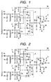
- Fig. 1 shows the construction of a two-band oscillating device of the invention, which comprises a first oscillator 1, a second oscillator 2, a coupled circuit 3 and an amplifier 4.
- the first oscillator 1 produces an oscillation signal in a first frequency band of low frequencies of 880 MHz to 940 MHz.
- the second oscillator 2 produces an oscillation signal in a second frequency band of 1805 MHz to 1920 MHz which is higher than the first frequency band.
- Each of the first and second oscillators 1 and 2 takes the form of a collector-grounded voltage-controlled Colpitts oscillator.
- a power supply voltage (Vb) is applied to either the first oscillator 1 or second oscillator 2 by a voltage switching means 5. The oscillator to which the power supply voltage is applied operates.
- the first oscillator 1 comprises a first oscillation transistor 1a, first feedback capacitors 1b and 1c, a first strip line 1d as an inductance device, and a first varactor diode 1e.
- the collector of the first oscillation transistor 1a is connected to the ground via a first grounding capacitor 1f so as to pass high frequencies.
- Vc applied to the first varactor diode 1e, the oscillation frequency in the first frequency band is changed and an oscillation signal is obtained from the emitter.
- the second oscillator 2 comprises a second oscillation transistor 2a, second feedback capacitors 2b and 2c, a second strip line 2d as an inductance device, and a second varactor diode 2e.
- the collector of the second oscillation transistor 2a is connected to the ground via a second grounding capacitor 2f so as to pass high frequencies.
- Vc applied to the first varactor diode 2e, the oscillation frequency in the second frequency band is changed and an oscillation signal is obtained from the emitter.
- the coupled circuit 3 has: first and second switching diodes 3a and 3b whose cathodes are connected to each other; a first coupling capacitor 3c connected between the anode of the first switching diode 3a and the emitter of the first oscillation transistor 1a; a second coupling capacitor 3d connected between the anode of the second switching diode 3b and the emitter of the second oscillation transistor 2a; a first feeding resistor 3e for connecting the collector of the first oscillation transistor 1a and the anode of the first switching diode 3a so as to pass almost direct currents; a second feeding resistor 3f for connecting the collector of the second oscillation transistor 2a and the anode of the second switching diode 3b so as to pass almost direct currents; and a choke inductor 3g for connecting the cathodes of the switching diodes 3a and 3b to the ground so as to pass almost direct currents.
- the amplifier 4 takes the form of an emitter-grounded aperiodic wide-band amplifier.
- a power supply voltage is applied to the collector of a transistor 4a for amplification via a choke inductor 4b.
- the emitter is connected to the ground via a bias resistor 4c and a bypass capacitor 4d.
- the base as an input terminal of the amplifier 4 is connected to the cathodes of the first and second switching diodes 3a and 3b via a DC blocking capacitor 4e.
- the first oscillator 1 when the power supply voltage is applied to the collector of the first oscillation transistor 1a by the voltage switching means 5, the first oscillator 1 operates, a current is passed through the first feeding resistor 3e, the first switching diode 3a and the choke inductor 3g, and the first switching diode 3a is made conductive (ON). Then, the oscillation signal appearing at the emitter of the first oscillation transistor 1a is supplied to the base of the transistor 4a for amplification via the first coupling capacitor 3c, first switching diode 3a and DC blocking capacitor 4e. The amplified oscillation signal is outputted from the collector of the transistor 4a for amplification via the DC blocking capacitor 4f.
- the second oscillator 2 When the power supply voltage is applied to the collector of the second oscillation transistor 2a by the voltage switching means 5, the second oscillator 2 operates. Simultaneously, a current is passed through the second feeding resistor 3f, second switching diode 3b and choke inductor 3g, so that the second switching diode 3b is made conductive (ON).
- the oscillation signal appearing at the emitter of the second oscillation transistor 2a is supplied to the base of the transistor 4a for amplification via the second coupling capacitor 3d, second switching diode 3b and DC blocking capacitor 4e. Simultaneously, the amplified oscillation signal is outputted from the collector of the transistor 4a for amplification via the DC blocking capacitor 4f.
- the oscillation signal in the first frequency band or the oscillation signal in the second frequency band is supplied to the amplifier 4 by the first switching diode 3a which is made conductive in association with the operating state of the first oscillator and the second switching diode 3b which is made conductive in association with the operating state of the second oscillator. Consequently, one of the switching diodes is certainly non-conducting and the first and second oscillators 1 and 2 are not coupled to each other. Therefore, one of the oscillators does not become a load on the other oscillator and the level of the oscillation signal supplied to the amplifier 4 is not reduced.
- Fig. 2 shows the construction of a modification of the two-band oscillating device of the invention.
- An inductor 3h is connected in series to the first coupling capacitor 3c connected to the first oscillator 1 for outputting the oscillation signal in the first frequency band which is low.
- a resistor 3i is connected in series to either the first coupling capacitor 3c or the second coupling capacitor 3d (the second coupling capacitor 3d in Fig. 2). Since the resistor 3i has the function of level adjustment, it is desirable to connect it to the coupling capacitor which is connected to the oscillator that produces the oscillation signal of a higher level.
- the other construction is similar to that shown in Fig. 1.
- the resonance frequency by the first coupling capacitor 3c and the inductor 3h is adjusted to an almost center frequency in the first frequency band.
- the passage of higher harmonics of the oscillation signal in the first frequency band is checked by the inductor 3h, so that the level of the oscillation signal supplied to the amplifier 4 is reduced.
- Fig. 3 shows the construction of another modification of the two-band oscillating device. Either the first switching diode 3a or the second switching diode 3b in the coupled circuit 3 in Fig. 1 is replaced by the resistor 3i. In association with the replacement, either the first resistor 3e or the second resistor 3f for voltage supply is eliminated. In Fig. 3, the second switching diode 3b in Fig. 1 is replaced by the resistor 3i and the second feeding resistor 3f is eliminated.
- the levels of the two oscillation signals to be supplied to the amplifier 4 can be adjusted. Since the coupling between the first and second oscillators 1 and 2 becomes loose by the resistor 3i, even when no switching diode (the second switching diode 3b in this case) is provided, reduction in level of the oscillation signal in the first frequency band is small.
- Fig. 4 shows the construction of further another modification of a two-band oscillating device.
- the first switching diode 3a in the coupled circuit 3 in Fig. 1 is replaced by the level adjusting resistor 3i.
- the resistor 3e for voltage supply is eliminated and the inductor 3h is connected in series to the first coupling capacitor 3c.
- the construction is suited to the case where the level of the oscillation signal in the first frequency band is higher than that of the oscillation signal in the second frequency band, and the frequency of the oscillation signal in the first frequency band is lower than that of the oscillation signal in the second frequency band.
- the other construction is the same as that of Fig. 1.
- the level of the oscillation signal in the first frequency band outputted from the first oscillator 1 can be adjusted.
- the level of higher harmonics of the oscillation signal in the first frequency band supplied to the amplifier 4 can be reduced by the inductor 3h connected in series to the first coupling capacitor 3c.
- voltage switching means for applying a power supply voltage to the first oscillator 1 or second oscillator 2 can be constructed by a switching diode or switching transistor.
- the two-band oscillating device of the invention comprises: the first switching diode connected in series between the first oscillator and the amplifier; and the second switching diode connected in series between the second oscillator and the amplifier.
- the anode of the first switching diode is connected to the collector of the first oscillation transistor so as to pass almost direct currents and is connected to the emitter via the first coupling capacitor
- the anode of the second switching diode is connected to the collector of the second oscillation transistor so as to pass almost direct currents and is connected to the emitter via the second coupling capacitor
- each of cathodes of the first and second switching diodes is connected to an input terminal of the amplifier and is also connected to the ground so as to pass almost direct currents
- the power supply voltage is applied to either the collector of the first oscillation transistor or the collector of the second oscillation transistor by the voltage switching means. Consequently, the operation of the oscillators and the conductive state of the switching diodes can be made associated with each other by the power source voltage applied to the collector of each of the oscillation transistors.
- a resistor is connected in series to either the first coupling capacitor or the second coupling capacitor.
- the resistor is connected to the coupling capacitor through which an oscillation signal of a higher level passes, the level of the oscillation signal supplied to the amplifier can be reduced.
- the levels of the two oscillation signals supplied to the amplifier can be matched.
- the two-band oscillating device of the invention comprises: the switching diode connected in series between the first oscillator and the amplifier; and the resistor connected in series between the second oscillator and the amplifier.
- the first oscillator is operated and the switching diode is made conductive. Consequently, the two oscillators can be loosely coupled to each other by one switching diode and the resistor, so that the cost can be reduced.
- the level of the oscillation signal in the second frequency band is higher tan that of the oscillation signal in the first frequency band, the level can be reduced by the resistor, thereby enabling the levels of the two oscillation signals supplied to the amplifier to be matched.
- the anode of the switching diode is connected to the collector of the first oscillation transistor so as to pass almost direct currents and is connected to the emitter via the first coupling capacitor.
- a resistor is connected in series between the cathode of the switching diode and the emitter of the second oscillation transistor, and the second coupling capacitor is connected in series to the resistor.
- the cathode of the switching diode is connected to the input terminal of the amplifier and is connected to the ground so as to pass almost direct currents.
- the power supply voltage is applied to either the collector of the first oscillation transistor or the collector of the second oscillation transistor by the voltage switching means.
- the switching diode can be made conductive in association with the operation of the first oscillator.
- the frequency of the oscillation signal in the first frequency band is set to be lower than that of the oscillation signal in the second frequency band
- an inductor is connected in series to the first coupling capacitor, and a resonance frequency by the first coupling capacitor and the inductor is set within the first frequency band. Consequently, passage of the higher harmonics of the oscillation signal in the first frequency band can be blocked by the inductor 3h.
- the amplifier is an amplifier of a wide band, the level of higher harmonics to be outputted is reduced and the occurrence of an interference signal in a mixer or the like connected at the next stage of the amplifier can be prevented.
Landscapes
- Inductance-Capacitance Distribution Constants And Capacitance-Resistance Oscillators (AREA)
- Oscillators With Electromechanical Resonators (AREA)
- Transceivers (AREA)
Applications Claiming Priority (4)
| Application Number | Priority Date | Filing Date | Title |
|---|---|---|---|
| JP23259799 | 1999-08-19 | ||
| JP23259799 | 1999-08-19 | ||
| JP2000017948 | 2000-01-24 | ||
| JP2000017948A JP2001127544A (ja) | 1999-08-19 | 2000-01-24 | 2バンド発振装置 |
Publications (2)
| Publication Number | Publication Date |
|---|---|
| EP1079512A1 true EP1079512A1 (fr) | 2001-02-28 |
| EP1079512B1 EP1079512B1 (fr) | 2004-06-09 |
Family
ID=26530545
Family Applications (1)
| Application Number | Title | Priority Date | Filing Date |
|---|---|---|---|
| EP00306529A Expired - Lifetime EP1079512B1 (fr) | 1999-08-19 | 2000-07-31 | Dispositif d'oscillateur à deux bandes |
Country Status (5)
| Country | Link |
|---|---|
| EP (1) | EP1079512B1 (fr) |
| JP (1) | JP2001127544A (fr) |
| KR (1) | KR100397113B1 (fr) |
| CN (1) | CN1134193C (fr) |
| DE (1) | DE60011356T2 (fr) |
Families Citing this family (7)
| Publication number | Priority date | Publication date | Assignee | Title |
|---|---|---|---|---|
| JP2002261543A (ja) | 2001-03-06 | 2002-09-13 | Alps Electric Co Ltd | 2バンド発振器 |
| JP3853285B2 (ja) | 2002-11-01 | 2006-12-06 | シャープ株式会社 | 電圧制御発振器及びこれを備えた集積回路装置 |
| JP5238633B2 (ja) | 2009-07-27 | 2013-07-17 | 株式会社東芝 | 半導体装置 |
| JP2011237467A (ja) * | 2010-04-30 | 2011-11-24 | Murata Mach Ltd | 画像形成装置 |
| CN104277765B (zh) | 2013-07-05 | 2017-12-08 | 中化蓝天集团有限公司 | 一种环保型近共沸混合制冷剂 |
| CN106877819B (zh) * | 2016-11-21 | 2020-08-11 | 成都仕芯半导体有限公司 | 基于复合型谐振器的压控振荡器 |
| CN106833536B (zh) | 2016-12-26 | 2019-08-20 | 浙江衢化氟化学有限公司 | 一种含有氢氟烯烃的制冷剂组合物 |
Citations (2)
| Publication number | Priority date | Publication date | Assignee | Title |
|---|---|---|---|---|
| JPH01173908A (ja) * | 1987-12-28 | 1989-07-10 | Hitachi Ltd | 発振装置 |
| EP0845855A2 (fr) * | 1996-11-27 | 1998-06-03 | TDK Corporation | Oscillateur commandé en tension |
-
2000
- 2000-01-24 JP JP2000017948A patent/JP2001127544A/ja not_active Withdrawn
- 2000-07-31 EP EP00306529A patent/EP1079512B1/fr not_active Expired - Lifetime
- 2000-07-31 DE DE60011356T patent/DE60011356T2/de not_active Expired - Fee Related
- 2000-08-14 CN CNB001215752A patent/CN1134193C/zh not_active Expired - Fee Related
- 2000-08-18 KR KR10-2000-0047796A patent/KR100397113B1/ko not_active Expired - Fee Related
Patent Citations (2)
| Publication number | Priority date | Publication date | Assignee | Title |
|---|---|---|---|---|
| JPH01173908A (ja) * | 1987-12-28 | 1989-07-10 | Hitachi Ltd | 発振装置 |
| EP0845855A2 (fr) * | 1996-11-27 | 1998-06-03 | TDK Corporation | Oscillateur commandé en tension |
Non-Patent Citations (1)
| Title |
|---|
| PATENT ABSTRACTS OF JAPAN vol. 013, no. 450 (E - 830) 11 October 1989 (1989-10-11) * |
Also Published As
| Publication number | Publication date |
|---|---|
| KR20010021353A (ko) | 2001-03-15 |
| DE60011356T2 (de) | 2005-06-09 |
| KR100397113B1 (ko) | 2003-09-06 |
| CN1134193C (zh) | 2004-01-07 |
| EP1079512B1 (fr) | 2004-06-09 |
| DE60011356D1 (de) | 2004-07-15 |
| CN1285699A (zh) | 2001-02-28 |
| JP2001127544A (ja) | 2001-05-11 |
Similar Documents
| Publication | Publication Date | Title |
|---|---|---|
| EP0803972B1 (fr) | Circuit oscillateur double bande | |
| EP0893878B1 (fr) | Circuit oscillateur haute fréquence | |
| US5418500A (en) | High-frequency oscillator circuit | |
| US5982243A (en) | Oscillator selectively operable with a parallel tuned or a series tuned resonant circuit | |
| KR960003560B1 (ko) | 전압제어 발진회로 | |
| EP1079512B1 (fr) | Dispositif d'oscillateur à deux bandes | |
| US6163222A (en) | Buffer amplifier with frequency selective mechanism | |
| JPH07107961B2 (ja) | テレビジョン受像機用局部発振器 | |
| US4731592A (en) | Voltage controllable oscillator | |
| US7538630B2 (en) | Voltage controlled oscillator | |
| US6271737B1 (en) | Communication device with feedback for cancellation of perturbations | |
| US5936480A (en) | Selective loading for sideband noise ratio reduction of a voltage controlled oscillator | |
| US6525619B1 (en) | Crystal-oscillator circuit for preventing stopping of oscillation | |
| US6624709B2 (en) | Voltage-controlled oscillator and electronic device using the same | |
| KR100372057B1 (ko) | 2밴드 발진기 | |
| US5859573A (en) | Circuit for separating the output of an oscillator from the other parts of a mobile communication system | |
| US6664862B2 (en) | Oscillator with constant output level over oscillation frequency range | |
| US20020158695A1 (en) | Low phase noise dual band voltage controlled oscillator | |
| JPH0555828A (ja) | 発振器 | |
| US7538624B2 (en) | Oscillator having multiple oscillation units | |
| JPH104315A (ja) | 高周波発振回路 | |
| EP1081846A1 (fr) | Oscillateur commandé en tension | |
| JP2001284964A (ja) | 発振器 | |
| KR930004660Y1 (ko) | 슈퍼 헤테로다인 수신회로 | |
| KR100386177B1 (ko) | 발진장치 |
Legal Events
| Date | Code | Title | Description |
|---|---|---|---|
| PUAI | Public reference made under article 153(3) epc to a published international application that has entered the european phase |
Free format text: ORIGINAL CODE: 0009012 |
|
| 17P | Request for examination filed |
Effective date: 20001123 |
|
| AK | Designated contracting states |
Kind code of ref document: A1 Designated state(s): DE FI FR SE |
|
| AX | Request for extension of the european patent |
Free format text: AL;LT;LV;MK;RO;SI |
|
| AKX | Designation fees paid |
Free format text: DE FI FR SE |
|
| 17Q | First examination report despatched |
Effective date: 20030327 |
|
| GRAP | Despatch of communication of intention to grant a patent |
Free format text: ORIGINAL CODE: EPIDOSNIGR1 |
|
| GRAS | Grant fee paid |
Free format text: ORIGINAL CODE: EPIDOSNIGR3 |
|
| GRAA | (expected) grant |
Free format text: ORIGINAL CODE: 0009210 |
|
| AK | Designated contracting states |
Kind code of ref document: B1 Designated state(s): DE FI FR SE |
|
| PG25 | Lapsed in a contracting state [announced via postgrant information from national office to epo] |
Ref country code: FI Free format text: LAPSE BECAUSE OF FAILURE TO SUBMIT A TRANSLATION OF THE DESCRIPTION OR TO PAY THE FEE WITHIN THE PRESCRIBED TIME-LIMIT Effective date: 20040609 |
|
| REF | Corresponds to: |
Ref document number: 60011356 Country of ref document: DE Date of ref document: 20040715 Kind code of ref document: P |
|
| PG25 | Lapsed in a contracting state [announced via postgrant information from national office to epo] |
Ref country code: SE Free format text: LAPSE BECAUSE OF FAILURE TO SUBMIT A TRANSLATION OF THE DESCRIPTION OR TO PAY THE FEE WITHIN THE PRESCRIBED TIME-LIMIT Effective date: 20040909 |
|
| ET | Fr: translation filed | ||
| PLBE | No opposition filed within time limit |
Free format text: ORIGINAL CODE: 0009261 |
|
| STAA | Information on the status of an ep patent application or granted ep patent |
Free format text: STATUS: NO OPPOSITION FILED WITHIN TIME LIMIT |
|
| 26N | No opposition filed |
Effective date: 20050310 |
|
| PGFP | Annual fee paid to national office [announced via postgrant information from national office to epo] |
Ref country code: FR Payment date: 20050719 Year of fee payment: 6 |
|
| PGFP | Annual fee paid to national office [announced via postgrant information from national office to epo] |
Ref country code: DE Payment date: 20050926 Year of fee payment: 6 |
|
| PG25 | Lapsed in a contracting state [announced via postgrant information from national office to epo] |
Ref country code: DE Free format text: LAPSE BECAUSE OF NON-PAYMENT OF DUE FEES Effective date: 20070201 |
|
| REG | Reference to a national code |
Ref country code: FR Ref legal event code: ST Effective date: 20070330 |
|
| PG25 | Lapsed in a contracting state [announced via postgrant information from national office to epo] |
Ref country code: FR Free format text: LAPSE BECAUSE OF NON-PAYMENT OF DUE FEES Effective date: 20060731 |