EP1079537A2 - Tragbares Endgerät - Google Patents
Tragbares Endgerät Download PDFInfo
- Publication number
- EP1079537A2 EP1079537A2 EP00118110A EP00118110A EP1079537A2 EP 1079537 A2 EP1079537 A2 EP 1079537A2 EP 00118110 A EP00118110 A EP 00118110A EP 00118110 A EP00118110 A EP 00118110A EP 1079537 A2 EP1079537 A2 EP 1079537A2
- Authority
- EP
- European Patent Office
- Prior art keywords
- sampling clock
- profile data
- portable terminal
- sampling
- correlator
- Prior art date
- Legal status (The legal status is an assumption and is not a legal conclusion. Google has not performed a legal analysis and makes no representation as to the accuracy of the status listed.)
- Granted
Links
Images


Classifications
-
- H—ELECTRICITY
- H04—ELECTRIC COMMUNICATION TECHNIQUE
- H04B—TRANSMISSION
- H04B1/00—Details of transmission systems, not covered by a single one of groups H04B3/00 - H04B13/00; Details of transmission systems not characterised by the medium used for transmission
- H04B1/69—Spread spectrum techniques
- H04B1/707—Spread spectrum techniques using direct sequence modulation
- H04B1/7073—Synchronisation aspects
- H04B1/7075—Synchronisation aspects with code phase acquisition
- H04B1/708—Parallel implementation
-
- H—ELECTRICITY
- H04—ELECTRIC COMMUNICATION TECHNIQUE
- H04B—TRANSMISSION
- H04B1/00—Details of transmission systems, not covered by a single one of groups H04B3/00 - H04B13/00; Details of transmission systems not characterised by the medium used for transmission
- H04B1/69—Spread spectrum techniques
- H04B1/707—Spread spectrum techniques using direct sequence modulation
- H04B1/7073—Synchronisation aspects
- H04B1/7075—Synchronisation aspects with code phase acquisition
- H04B1/70757—Synchronisation aspects with code phase acquisition with increased resolution, i.e. higher than half a chip
-
- H—ELECTRICITY
- H04—ELECTRIC COMMUNICATION TECHNIQUE
- H04B—TRANSMISSION
- H04B1/00—Details of transmission systems, not covered by a single one of groups H04B3/00 - H04B13/00; Details of transmission systems not characterised by the medium used for transmission
- H04B1/69—Spread spectrum techniques
- H04B1/707—Spread spectrum techniques using direct sequence modulation
- H04B1/709—Correlator structure
-
- H—ELECTRICITY
- H04—ELECTRIC COMMUNICATION TECHNIQUE
- H04B—TRANSMISSION
- H04B2201/00—Indexing scheme relating to details of transmission systems not covered by a single group of H04B3/00 - H04B13/00
- H04B2201/69—Orthogonal indexing scheme relating to spread spectrum techniques in general
- H04B2201/707—Orthogonal indexing scheme relating to spread spectrum techniques in general relating to direct sequence modulation
- H04B2201/70703—Orthogonal indexing scheme relating to spread spectrum techniques in general relating to direct sequence modulation using multiple or variable rates
Definitions
- the present invention relates to a portable terminal for use in a mobile communication system based on the CDMA (Code Division Multiple Access) technique, and more particularly to a portable terminal that is capable of reducing power consumption in the generation of profile data.
- CDMA Code Division Multiple Access
- a portable terminal for use in a CDMA mobile communication system receives a signal transmitted via a radio link, it despreads the received signal and outputs audio or video data based on the despread signal. Though it is necessary to recognize the timing of transmission of the signal from the base station, the portable terminal is unable to recognize the timing of transmission of the signal from the base station.
- the portable terminal In order to detect a point (timing) to start despreading the received signal, it has been customary for the portable terminal to calculate correlated values between a plurality of known patterns that have been internally generated and the received data, generate profile data based on the calculated correlated values, and detect the timing to start despreading the received signal from a peak value of the profile data.
- the portable terminal for use in the CDMA mobile communication system has heretofore been required to reduce power consumption because it performs a transmission power control process and other complex control processes.
- the accuracy with which to detect a received pilot signal required to generate profile data in the above conventional portable terminal may be increased by increasing the number of sampling points.
- increasing the number of sampling points results in an increase in the power consumption by the portable terminal.
- a portable terminal has a level detector which compares profile data generated by a profile generator with a threshold value, and determines a sampling rate for a correlating process performed by a correlator based on the result of the comparison.
- the sampling rate is determined in order to increase the sampling rate at profile points in excess of the threshold value, of the profile data. Therefore, profile data is generated highly accurately at a higher sampling clock rate at points which require a higher accuracy, and profile data is generated at a lower sampling clock rate at points which do not require such a higher accuracy.
- Fig. 1 shows in block form a portion of a portable terminal according to the present invention for detecting a received pilot signal and generating profile data.
- the portable terminal comprises correlator 10 for performing a correlating process to calculate correlated values between a received pilot signal and a plurality of known patterns that have been internally generated in timed relation to a supplied sampling clock signal, and output the calculated correlated values as correlated data, profile generator 30 for correcting the level of the correlated data outputted from correlator 10 and calculating a power value thereby to generate and output profile data, level detector 40 for comparing the profile data outputted from profile generator 30 with a predetermined threshold value, and determining a sampling rate for the correlating process performed by correlator 10 based on the result of the comparison, and sampling clock generator 20 for generating and outputting a sampling clock signal to be supplied to correlator 10 based on the determined sampling rate outputted from level detector 40. Correlator 10 performs the correlating process in timed relation to the sampling clock signal generated by the sampling clock generator 20.
- correlator 10 comprises replica generator 11 for generating and outputting a known pattern for calculating a correlated value between itself and the received pilot signal, a plurality of delay elements 12-1 through 12-(n-1) for delaying the known pattern outputted from replica generator 11 by a predetermined time and outputting the delayed patterns, a plurality of correlating units 13-1 through 13-n for correlating and adding the received pilot signal and the known pattern outputted from replica generator 11 and the known patterns delayed by the respective delay elements 12-1 through 12-(n-1), and outputting the added results as correlated data, and timing generator 14 for supplying the sampling clock signal outputted from sampling clock generator 20 to correlating units 13-1 through 13-n.
- profile generator 30 comprises level corrector 31 for correcting the level of the correlated data outputted from correlator 10, power calculator 32 for calculating the power value of the correlated data whose level has been corrected by level corrector 31 thereby to generate profile data, and average calculator 33 for calculating an average value during a certain interval of the profile data generated by the power calculator 32 as occasion arises.
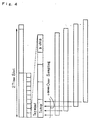
- Fig. 4 is illustrative of a correlating process performed by correlator 10 shown in Fig. 2.
- Correlating unit 13-1 in correlator 10 multiplies the received pilot signal by the known pattern generated by replica generator 11 at each of pulses of the sampling clock signal from timing generator 14, adds products at the respective pulses of the sampling clock signal, and outputs the sum as correlated data.
- Correlating units 13-2 through 13-n multiply the received pilot signal by the known patterns generated by replica generator 11 and delayed by delay elements 12-1 through 12-(n-1) at each of the pulses of the sampling clock signal from timing generator 14, adds products at the respective pulses of the sampling clock signal, and outputs the sums as correlated data.
- the correlating process performed by correlator 10 needs to be carried out on N chips per symbol, and a C-times oversampling process is effected for increased detection accuracy.
- n correlating units are employed for simultaneous processing as shown in Fig. 2.
- the known pattern generated by the replica generator 11 is delayed 1/C chip by delay elements 12-1 through 12-(n-1).
- the correlated data outputted from correlator 10 is supplied to profile generator 30.
- level corrector 31 corrects the level of the correlated data in order to remove a level variation error due to AGC (Automatic Gain Control) characteristics of a radio unit (not shown).
- AGC Automatic Gain Control
- power calculator 32 calculates a power value of the correlated data whose level has been corrected by level corrector 31 thereby to generate profile data.
- Average calculator 33 is used to calculate average profile data over several slots.
- the profile data generated by profile generator 30 is supplied to level detector 40 when next profile data is generated by profile generator 30.
- Fig. 5 shows an operation sequence of level detector 40 in the portable terminal shown in Fig. 1.
- the profile data generated by profile generator 30 is supplied to level detector 40 in step S1. Then, level detector 40 decides whether the sampling clock signal for determining a sampling rate in correlator 10 is to be automatically controlled or not in step S2.
- level detector 40 determines the accuracy with which to detect the received pilot signal in correlator 10 in step S3.
- step S3 If the detection accuracy is determined to be lower in step S3, then the sampling clock signal to be supplied to correlator 10 is determined to be of a lower clock rate (C times) in step S4. Then, level detector 40 outputs a control signal for generating the sampling clock signal to sampling clock generator 20 in step S8. Therefore, profile data is generated with a lower power.
- step S3 If the detection accuracy is determined to be higher in step S3, then the sampling clock signal to be supplied to correlator 10 is determined to be of a higher clock rate (a times) in step S5. Then, level detector 40 outputs a control signal for generating the sampling clock signal to sampling clock generator 20 in step S8. Therefore, profile data is generated with a normal power.
- level detector 40 compares the profile data generated by profile generator 30 with a predetermined threshold value in step S6, and determines a sampling clock signal for increasing the sampling rate, i.e., increasing the accuracy, in correlator 10 only around profile points in excess of the threshold value, of the profile data in the step S7. Thereafter, level detector 40 outputs a control signal for generating the sampling clock signal to sampling clock generator 20 in step S8.
- Sampling clock generator 20 generates the sampling clock signal based on the control signal that has been supplied from level detector 40 in step S8.
- Correlator 10 performs its correlating process at a sampling rate based on the generated sampling clock signal.
- Fig. 6a shows mth profile data generated by the portable terminal shown in Fig. 1
- Fig. 6b shows (m +1)th profile data generated by the portable terminal shown in Fig. 1.
- the profile data shown in Fig. 6a is generated if the sampling clock signal is determined to be of the lower clock rate (C times) in step S4 shown in Fig. 5.
- Sampling clock generator 20 supplies a sampling clock signal having an X-times (X > C) sampling rate to correlator 10 only around points in excess of the threshold level of the mth profile data shown in Fig. 6, and correlator 10 correlates the received pilot signal using the supplied sampling clock signal.
- the (m +1)th profile data includes regions enclosed by the broken lines which are made more accurate by X-times oversampling, making it possible to obtain profile data with lower power consumption.
- sampling clock generator 20 generates a sampling clock signal whose sampling rate is controlled based on the level of the profile data detected by the level detector 40, and correlator 10 correlates the received pilot signal with the generated sampling clock signal.
- Fig. 7 shows another operation sequence of level detector 40 in the portable terminal shown in Fig. 1.
- Correlator 10 performs a correlating process in step S11. Then, level detector 40 decides whether the sampling clock signal for determining a sampling rate in correlator 10 is to be automatically controlled or not in step S12.
- level detector 40 determines the accuracy with which to detect the received pilot signal in correlator 10 in step S13.
- step S13 If the detection accuracy is determined to be lower in step S13, then the sampling clock signal to be supplied to correlator 10 is determined to be of a lower clock rate (C times) in step S14. Therefore, profile data is generated with a lower power.
- step S13 If the detection accuracy is determined to be higher in step S13, then the sampling clock signal to be supplied to correlator 10 is determined to be of a higher clock rate (a times) in step S15. Therefore, profile data is generated with a normal power.
- correlator 10 calculates correlated data, and profile generator 30 generates profile data based on the correlated data calculated by correlator 10.
- level detector 40 compares the profile data generated by profile generator 30 with a predetermined threshold value in step S17. If the profile data exceeds the threshold value, then level detector 40 determines a sampling clock signal for increasing the sampling rate, i.e., increasing the accuracy, in the subsequent correlating process in correlator 10 in step S18. Thereafter, level detector 40 outputs a control signal for generating the sampling clock signal to sampling clock generator 20. The number of correlating points is increased to generate profile data of higher accuracy.
- the sampling clock signal to be supplied to correlator 10 is determined to be of a lower clock rate (C times) in step S14.
- profile data is generated with higher accuracy only in regions enclosed by the broken lines which exceed the threshold level.
- the operation sequence shown in Fig. 7 offers another advantage in that profile data can be generated with a lower power even without the mth profile data.
- a plurality of threshold values may be used to determine a sampling clock signal. Use of such a plurality of threshold values to determine a sampling clock signal will be described below.
- Fig. 9 shows still another operation sequence of level detector 40 in the portable terminal shown in Fig. 1.
- the profile data generated by profile generator 30 is supplied to level detector 40 in step S21. Then, Level detector 40 decides whether the sampling clock signal for determining a sampling rate in correlator 10 is to be automatically controlled or not in step S22.
- level detector 40 determines the accuracy with which to detect the received pilot signal in correlator 10 in step S23.
- step S23 If the detection accuracy is determined to be lower in step S23, then the sampling clock signal to be supplied to correlator 10 is determined to be of a lower clock rate (C times) in step S24.
- Level detector 40 outputs a control signal for generating the sampling clock signal to sampling clock generator 20 in step S30. Therefore, profile data is generated with a lower power.
- step S13 If the detection accuracy is determined to be higher in step S13, then the sampling clock signal to be supplied to correlator 10 is determined to be of a higher clock rate (a times) in step S25.
- Level detector 40 outputs a control signal for generating the sampling clock signal to sampling clock generator 20 in step S30. Therefore, profile data is generated with a normal power.
- the sampling clock signal to be supplied to correlator 10 is determined to be of a higher clock rate (a times) in step S28.
- Level detector 40 outputs a control signal for generating the sampling clock signal to sampling clock generator 20 in step S30.
- the sampling clock signal to be supplied to correlator 10 is determined to be of a lower clock rate (C times) in step S24.
- Level detector 40 outputs a control signal for generating the sampling clock signal to sampling clock generator 20 in step S30.
- the sampling rates d, a, C are related by d > a > C.
- the above operation sequence makes it possible to further increase the sampling rate for necessary points, allowing more detailed profile data to be acquired.
- Three or more threshold values may be used to change sampling rates.
- the level or threshold value for determining an oversampling rate may be changed each time profile data is to be determined, or an arrangement for changing sampling rates may be employed.
- the portable terminal has the level detector which compares profile data generated by the profile generator with a threshold value, and determines a sampling rate in order to increase the sampling rate at profile points in excess of the threshold value, of the profile data. Therefore, profile data is generated at a higher sampling clock rate at points which require a higher accuracy, and profile data is generated at a lower sampling clock rate at points which do not require such a higher accuracy, by reducing the number of sampling points. Accordingly, highly accurate profile data can be generated while at the same time the power consumption is reduced and the circuit scale of the portable terminal is reduced.
Landscapes
- Engineering & Computer Science (AREA)
- Computer Networks & Wireless Communication (AREA)
- Signal Processing (AREA)
- Mobile Radio Communication Systems (AREA)
- Synchronisation In Digital Transmission Systems (AREA)
- Radar Systems Or Details Thereof (AREA)
- Dc Digital Transmission (AREA)
Applications Claiming Priority (2)
| Application Number | Priority Date | Filing Date | Title |
|---|---|---|---|
| JP23998399A JP3412689B2 (ja) | 1999-08-26 | 1999-08-26 | 携帯電話機 |
| JP23998399 | 1999-08-26 |
Publications (3)
| Publication Number | Publication Date |
|---|---|
| EP1079537A2 true EP1079537A2 (de) | 2001-02-28 |
| EP1079537A3 EP1079537A3 (de) | 2001-11-07 |
| EP1079537B1 EP1079537B1 (de) | 2003-04-23 |
Family
ID=17052741
Family Applications (1)
| Application Number | Title | Priority Date | Filing Date |
|---|---|---|---|
| EP20000118110 Expired - Lifetime EP1079537B1 (de) | 1999-08-26 | 2000-08-25 | Tragbares Endgerät |
Country Status (6)
| Country | Link |
|---|---|
| US (1) | US6693955B1 (de) |
| EP (1) | EP1079537B1 (de) |
| JP (1) | JP3412689B2 (de) |
| CN (1) | CN1166094C (de) |
| AU (1) | AU766431B2 (de) |
| DE (1) | DE60002268T2 (de) |
Cited By (5)
| Publication number | Priority date | Publication date | Assignee | Title |
|---|---|---|---|---|
| US6693955B1 (en) * | 1999-08-26 | 2004-02-17 | Nec Corporation | Portable terminal |
| EP1309096A4 (de) * | 2001-06-01 | 2005-03-16 | Sony Corp | Vorrichtung für ein spreizspektrum-kommunikationssystem |
| WO2007086858A1 (en) * | 2006-01-27 | 2007-08-02 | Thomson Licensing | Method and apparatus for multiresolution / multipath searcher |
| WO2007125168A1 (en) * | 2006-04-27 | 2007-11-08 | Nokia Corporation | Signal detection in ofdm system |
| US8045927B2 (en) | 2006-04-27 | 2011-10-25 | Nokia Corporation | Signal detection in multicarrier communication system |
Families Citing this family (14)
| Publication number | Priority date | Publication date | Assignee | Title |
|---|---|---|---|---|
| CN1175695C (zh) * | 2000-01-12 | 2004-11-10 | 三菱电机株式会社 | 移动通信终端 |
| US7197098B2 (en) * | 2000-12-29 | 2007-03-27 | Intel Corporation | High-speed serial data recovery |
| DE60239718D1 (de) | 2001-02-09 | 2011-05-26 | Canon Kk | Informationsverarbeitungsgerät und seine Steuerverfahren, Computerprogramm, und Speichermedium |
| US8391249B2 (en) | 2003-02-18 | 2013-03-05 | Qualcomm Incorporated | Code division multiplexing commands on a code division multiplexed channel |
| US8150407B2 (en) | 2003-02-18 | 2012-04-03 | Qualcomm Incorporated | System and method for scheduling transmissions in a wireless communication system |
| US7660282B2 (en) | 2003-02-18 | 2010-02-09 | Qualcomm Incorporated | Congestion control in a wireless data network |
| US8023950B2 (en) | 2003-02-18 | 2011-09-20 | Qualcomm Incorporated | Systems and methods for using selectable frame durations in a wireless communication system |
| US7155236B2 (en) | 2003-02-18 | 2006-12-26 | Qualcomm Incorporated | Scheduled and autonomous transmission and acknowledgement |
| US8081598B2 (en) | 2003-02-18 | 2011-12-20 | Qualcomm Incorporated | Outer-loop power control for wireless communication systems |
| US7215930B2 (en) | 2003-03-06 | 2007-05-08 | Qualcomm, Incorporated | Method and apparatus for providing uplink signal-to-noise ratio (SNR) estimation in a wireless communication |
| US8705588B2 (en) | 2003-03-06 | 2014-04-22 | Qualcomm Incorporated | Systems and methods for using code space in spread-spectrum communications |
| US8477592B2 (en) | 2003-05-14 | 2013-07-02 | Qualcomm Incorporated | Interference and noise estimation in an OFDM system |
| US8489949B2 (en) | 2003-08-05 | 2013-07-16 | Qualcomm Incorporated | Combining grant, acknowledgement, and rate control commands |
| US20070248191A1 (en) * | 2006-04-25 | 2007-10-25 | Telefonaktiebolaget Lm Ericsson (Publ) | Baseband sample selection |
Family Cites Families (19)
| Publication number | Priority date | Publication date | Assignee | Title |
|---|---|---|---|---|
| FR2273362A1 (en) | 1974-05-31 | 1975-12-26 | Alsthom Cgee | High voltage circuit breaker - has fixed contact with semi-mobile contact movable from mobile contact by spring |
| JPS6193746A (ja) | 1984-10-12 | 1986-05-12 | Sony Corp | スペクトラム拡散通信復調装置 |
| US4910752A (en) * | 1987-06-15 | 1990-03-20 | Motorola, Inc. | Low power digital receiver |
| US5465405A (en) * | 1992-07-30 | 1995-11-07 | Raytheon Company | Apparatus and method for detecting signals |
| US5841808A (en) * | 1995-03-23 | 1998-11-24 | Mcdonnell Douglas Corporation | Spread spectrum chip rate tracking system |
| JP3030230B2 (ja) | 1995-06-06 | 2000-04-10 | 松下電器産業株式会社 | 拡散通信システムの受信装置 |
| FR2737362B1 (fr) * | 1995-07-25 | 1997-10-10 | Matra Communication | Procede de selection des retards de propagation retenus pour recevoir des messages transmis par radiocommunication a etalement de spectre |
| US6118808A (en) * | 1996-07-12 | 2000-09-12 | General Electric Company | GPS receiver with efficient signal acquisition |
| JPH10145326A (ja) | 1996-11-14 | 1998-05-29 | Fujitsu Ltd | Cdmaシステム用受信装置 |
| US5864315A (en) * | 1997-04-07 | 1999-01-26 | General Electric Company | Very low power high accuracy time and frequency circuits in GPS based tracking units |
| JP3408944B2 (ja) | 1997-04-24 | 2003-05-19 | シャープ株式会社 | スペクトル直接拡散通信システムにおける復調装置及び同システムにおける相関器 |
| JP3751419B2 (ja) | 1997-06-16 | 2006-03-01 | 松下電器産業株式会社 | マッチドフィルタおよび同期方法 |
| JP2856249B2 (ja) | 1997-06-24 | 1999-02-10 | 日本電気株式会社 | Cdma同期捕捉回路 |
| JP3159378B2 (ja) | 1997-08-13 | 2001-04-23 | 日本電気株式会社 | スペクトル拡散通信方式 |
| JP3793632B2 (ja) | 1997-12-18 | 2006-07-05 | 松下電器産業株式会社 | セルサーチ方法及び移動局装置 |
| JP3308481B2 (ja) * | 1998-01-09 | 2002-07-29 | 沖電気工業株式会社 | 相関値算出装置 |
| DE19824218C1 (de) | 1998-05-29 | 2000-03-23 | Ericsson Telefon Ab L M | Multipfad-Ausbreitungsverzögerungs-Bestimmungsvorrichtung unter Verwendung von periodisch eingefügten Pilotsymbolen |
| JP3412689B2 (ja) * | 1999-08-26 | 2003-06-03 | 日本電気株式会社 | 携帯電話機 |
| US6292748B1 (en) * | 2000-07-14 | 2001-09-18 | General Electric Company | Reduction of time error in GPS localization without a highly accurate clock |
-
1999
- 1999-08-26 JP JP23998399A patent/JP3412689B2/ja not_active Expired - Fee Related
-
2000
- 2000-08-24 AU AU53596/00A patent/AU766431B2/en not_active Ceased
- 2000-08-24 CN CNB001236784A patent/CN1166094C/zh not_active Expired - Fee Related
- 2000-08-25 EP EP20000118110 patent/EP1079537B1/de not_active Expired - Lifetime
- 2000-08-25 DE DE2000602268 patent/DE60002268T2/de not_active Expired - Lifetime
- 2000-08-25 US US09/645,568 patent/US6693955B1/en not_active Expired - Lifetime
Cited By (9)
| Publication number | Priority date | Publication date | Assignee | Title |
|---|---|---|---|---|
| US6693955B1 (en) * | 1999-08-26 | 2004-02-17 | Nec Corporation | Portable terminal |
| EP1309096A4 (de) * | 2001-06-01 | 2005-03-16 | Sony Corp | Vorrichtung für ein spreizspektrum-kommunikationssystem |
| EP1601115A3 (de) * | 2001-06-01 | 2006-04-12 | Sony Corporation | Vorrichtung für ein Spreizspektrum-Kommunikationssystem |
| US7283581B2 (en) | 2001-06-01 | 2007-10-16 | Sony Corporation | Spread spectrum communication system apparatus |
| WO2007086858A1 (en) * | 2006-01-27 | 2007-08-02 | Thomson Licensing | Method and apparatus for multiresolution / multipath searcher |
| US8340159B2 (en) | 2006-01-27 | 2012-12-25 | Thomson Licensing | Method and apparatus for multiresolution / multipath searcher |
| WO2007125168A1 (en) * | 2006-04-27 | 2007-11-08 | Nokia Corporation | Signal detection in ofdm system |
| US7864884B2 (en) | 2006-04-27 | 2011-01-04 | Nokia Corporation | Signal detection in OFDM system |
| US8045927B2 (en) | 2006-04-27 | 2011-10-25 | Nokia Corporation | Signal detection in multicarrier communication system |
Also Published As
| Publication number | Publication date |
|---|---|
| CN1286545A (zh) | 2001-03-07 |
| US6693955B1 (en) | 2004-02-17 |
| EP1079537B1 (de) | 2003-04-23 |
| DE60002268T2 (de) | 2004-01-15 |
| AU766431B2 (en) | 2003-10-16 |
| CN1166094C (zh) | 2004-09-08 |
| EP1079537A3 (de) | 2001-11-07 |
| DE60002268D1 (de) | 2003-05-28 |
| JP3412689B2 (ja) | 2003-06-03 |
| JP2001069568A (ja) | 2001-03-16 |
| HK1037435A1 (en) | 2002-02-08 |
| AU5359600A (en) | 2001-03-01 |
Similar Documents
| Publication | Publication Date | Title |
|---|---|---|
| EP1079537B1 (de) | Tragbares Endgerät | |
| US6724806B2 (en) | Variable rate transmission and reception methods, and variable rate transmission and reception devices | |
| CA2308425C (en) | Device and method for communicating reverse pilot signal in mobile communication system | |
| EP0951148A2 (de) | Synchronisiergerät und -verfahren für Direktsequenzspreizspektrumnachrichtenübertragung | |
| KR100307888B1 (ko) | 호 동안의 오정렬을 방지하는 다중 탐색 윈도우를 갖는 확산 스펙트럼 수신기 | |
| KR100361408B1 (ko) | Cdma 통신을 위한 동기포착회로 | |
| CA2276430C (en) | Method and apparatus for receiving spread spectrum signal | |
| US6704552B1 (en) | Mobile communication apparatus with an automatic frequency controller | |
| KR100294313B1 (ko) | 씨디엠에이수신기 | |
| US20040106421A1 (en) | Communication device | |
| US7907591B2 (en) | Synchronization detecting circuit and multimode wireless communication apparatus | |
| US6785257B1 (en) | Base station | |
| US6650693B1 (en) | Complex type correlator in CDMA system and initial synchronization acquiring method using the same | |
| KR100311515B1 (ko) | 이동통신시스템셀탐색장치및방법 | |
| US7720648B2 (en) | Method and apparatus for adapting threshold values in electronic signal processing devices | |
| US6850507B1 (en) | Apparatus and method for acquiring PN sequence in multicarrier CDMA mobile communication system | |
| JP2859604B2 (ja) | スライディング相関器 | |
| US7042924B2 (en) | Synchronization establishing and tracking circuit for CDMA base station | |
| JP2000278176A (ja) | 遅延プロファイル測定装置 | |
| HK1037435B (en) | Portable terminal | |
| JPH09284178A (ja) | 間欠動作型遅延ロックループ | |
| JP3258944B2 (ja) | 移動無線受信装置 | |
| JP4012520B2 (ja) | アレイアンテナ通信装置及び制御方法 | |
| KR100640337B1 (ko) | 부호분할 다중접속 방식을 사용하는 이동통신 시스템의 역확산장치 | |
| JP2003318780A (ja) | パス補足方法及びこの方法を利用するcdma受信装置 |
Legal Events
| Date | Code | Title | Description |
|---|---|---|---|
| PUAI | Public reference made under article 153(3) epc to a published international application that has entered the european phase |
Free format text: ORIGINAL CODE: 0009012 |
|
| AK | Designated contracting states |
Kind code of ref document: A2 Designated state(s): DE FR GB IT Kind code of ref document: A2 Designated state(s): AT BE CH CY DE DK ES FI FR GB GR IE IT LI LU MC NL PT SE |
|
| AX | Request for extension of the european patent |
Free format text: AL;LT;LV;MK;RO;SI |
|
| PUAL | Search report despatched |
Free format text: ORIGINAL CODE: 0009013 |
|
| AK | Designated contracting states |
Kind code of ref document: A3 Designated state(s): AT BE CH CY DE DK ES FI FR GB GR IE IT LI LU MC NL PT SE |
|
| AX | Request for extension of the european patent |
Free format text: AL;LT;LV;MK;RO;SI |
|
| 17P | Request for examination filed |
Effective date: 20011004 |
|
| AKX | Designation fees paid |
Free format text: DE FR GB IT |
|
| GRAH | Despatch of communication of intention to grant a patent |
Free format text: ORIGINAL CODE: EPIDOS IGRA |
|
| GRAH | Despatch of communication of intention to grant a patent |
Free format text: ORIGINAL CODE: EPIDOS IGRA |
|
| GRAA | (expected) grant |
Free format text: ORIGINAL CODE: 0009210 |
|
| AK | Designated contracting states |
Designated state(s): DE FR GB IT |
|
| REG | Reference to a national code |
Ref country code: GB Ref legal event code: FG4D |
|
| REF | Corresponds to: |
Ref document number: 60002268 Country of ref document: DE Date of ref document: 20030528 Kind code of ref document: P |
|
| ET | Fr: translation filed | ||
| PLBE | No opposition filed within time limit |
Free format text: ORIGINAL CODE: 0009261 |
|
| STAA | Information on the status of an ep patent application or granted ep patent |
Free format text: STATUS: NO OPPOSITION FILED WITHIN TIME LIMIT |
|
| 26N | No opposition filed |
Effective date: 20040126 |
|
| PGFP | Annual fee paid to national office [announced via postgrant information from national office to epo] |
Ref country code: FR Payment date: 20110818 Year of fee payment: 12 Ref country code: DE Payment date: 20110817 Year of fee payment: 12 Ref country code: GB Payment date: 20110824 Year of fee payment: 12 |
|
| PGFP | Annual fee paid to national office [announced via postgrant information from national office to epo] |
Ref country code: IT Payment date: 20110823 Year of fee payment: 12 |
|
| GBPC | Gb: european patent ceased through non-payment of renewal fee |
Effective date: 20120825 |
|
| REG | Reference to a national code |
Ref country code: FR Ref legal event code: ST Effective date: 20130430 |
|
| PG25 | Lapsed in a contracting state [announced via postgrant information from national office to epo] |
Ref country code: IT Free format text: LAPSE BECAUSE OF NON-PAYMENT OF DUE FEES Effective date: 20120825 |
|
| PG25 | Lapsed in a contracting state [announced via postgrant information from national office to epo] |
Ref country code: DE Free format text: LAPSE BECAUSE OF NON-PAYMENT OF DUE FEES Effective date: 20130301 Ref country code: GB Free format text: LAPSE BECAUSE OF NON-PAYMENT OF DUE FEES Effective date: 20120825 |
|
| PG25 | Lapsed in a contracting state [announced via postgrant information from national office to epo] |
Ref country code: FR Free format text: LAPSE BECAUSE OF NON-PAYMENT OF DUE FEES Effective date: 20120831 |
|
| REG | Reference to a national code |
Ref country code: DE Ref legal event code: R119 Ref document number: 60002268 Country of ref document: DE Effective date: 20130301 |