EP1079666A2 - Organische elektrolumineszente Vorrichtung - Google Patents
Organische elektrolumineszente Vorrichtung Download PDFInfo
- Publication number
- EP1079666A2 EP1079666A2 EP00306544A EP00306544A EP1079666A2 EP 1079666 A2 EP1079666 A2 EP 1079666A2 EP 00306544 A EP00306544 A EP 00306544A EP 00306544 A EP00306544 A EP 00306544A EP 1079666 A2 EP1079666 A2 EP 1079666A2
- Authority
- EP
- European Patent Office
- Prior art keywords
- organic
- aluminum
- quinolinolato
- layer
- glass transition
- Prior art date
- Legal status (The legal status is an assumption and is not a legal conclusion. Google has not performed a legal analysis and makes no representation as to the accuracy of the status listed.)
- Withdrawn
Links
Images
Classifications
-
- H—ELECTRICITY
- H05—ELECTRIC TECHNIQUES NOT OTHERWISE PROVIDED FOR
- H05B—ELECTRIC HEATING; ELECTRIC LIGHT SOURCES NOT OTHERWISE PROVIDED FOR; CIRCUIT ARRANGEMENTS FOR ELECTRIC LIGHT SOURCES, IN GENERAL
- H05B33/00—Electroluminescent light sources
- H05B33/02—Details
- H05B33/04—Sealing arrangements, e.g. against humidity
-
- H—ELECTRICITY
- H10—SEMICONDUCTOR DEVICES; ELECTRIC SOLID-STATE DEVICES NOT OTHERWISE PROVIDED FOR
- H10K—ORGANIC ELECTRIC SOLID-STATE DEVICES
- H10K59/00—Integrated devices, or assemblies of multiple devices, comprising at least one organic light-emitting element covered by group H10K50/00
- H10K59/80—Constructional details
- H10K59/87—Passivation; Containers; Encapsulations
- H10K59/874—Passivation; Containers; Encapsulations including getter material or desiccant
Definitions
- the present invention relates generally to an organic EL device using an organic compound, and more specifically to improvements in or relating to a sealing structure for an organic EL structure stacked on a substrate and an organic material forming a light emitting layer, etc.
- organic EL devices have been under intensive investigation.
- One such device is basically built up of a thin film form of hole transporting material such as triphenyldiamine (TPD) deposited by evaporation on a hole injecting electrode, a light emitting layer of fluorescent material such as an aluminum quinolinol complex (Alq 3 ) laminated thereon, and a metal (electron injecting) electrode of a metal having a low work function such as Mg and formed on the light emitting layer.
- TPD triphenyldiamine
- Alq 3 aluminum quinolinol complex
- Mg metal having a low work function
- An organic EL device is now known to deteriorate due to moisture. Exposure of the organic EL device to moisture, for instance, causes a light emitting layer to peel off electrode layers, or materials forming part thereof to degenerate. This results in another problem that non-light emission spots called dark spots occur with a light emitting area decrease or any consistent light emission cannot be kept.
- JP-A 3-261091 discloses that diphosphorus pentaoxide (P 2 O 5 ) is used as the drying agent.
- P 2 O 5 absorbs water and dissolves (deliquesces) in the water to form phosphoric acid having an adverse influence on the organic EL structure.
- P 2 O 5 is also impractical because some considerable limitations are imposed on how to seal it in the case.
- JP-A 6-176867 discloses an organic EL device with a finely divided solid dehydrating agent filled in an outside protective case.
- the publication refers to zeolite, activated alumina, silica gel, calcium oxide, etc.
- the fabrication process becomes clumsy due to the need of steps for filling the finely divided solid dehydrating agent in the outside case, and mounting the outside case with the finely divided solid dehydrating agent filled therein.
- JP-A 9-148066 shows a compound that serves as a drying agent chemically adsorbing water and remains solid even upon moisture adsorption, e.g., alkaline metal oxides, alkaline earth metal oxides, sulfates and metal halides. These compounds are capable of chemically adsorbing moisture with no re-release of the moisture and so ensures increased device life. However, not only is it difficult to hold the solid drying agent in the airtight case but also an additional step is needed for that purpose. The resulting device is still less than satisfactory in terms of life.
- JP-A's 5-114486 and 5-41281 disclose a method for storing a device in an inert liquid compound comprising a dehydrating agent-containing fluorinated hydrocarbon. Although this method has some effects on the protection of an organic El device against moisture, yet the need of providing a step of pouring the dehydrating agent-containing inert liquid compound makes the sealing process clumsy.
- An outstanding problem with an organic EL device is that even when it has satisfactory initial light emission performance, it deteriorates with the lapse of time; any good light emission performance cannot be maintained over an extended period of time. Thus, how to prevent deterioration of the device is a significant challenge, and so has already been studied from every direction.
- Device deterioration is caused by various factors; for instance, the device deteriorates through reactions of an electron injecting electrode of high reactivity with the air and moisture, and due to degradation of an interface between a hole injecting electrode and an organic layer and degradation of the organic layer itself. All-around improvements in those physical properties are of great importance to achieve improvements in device life and light emission performance.
- JP-A 5-182764 shows that an organic compound layer is formed by vacuum evaporation and this layer is heated at a temperature that is higher than 50°C and lower than the melting point thereof to form a light emitting layer that has a crystallite structure produced by heating.
- the heating temperatures set forth in the examples of the publication are only 180 to 200°C and 120°C; any experimentation was not carried out concerning heating at other temperatures.
- the description of the crystallite structure is moot, it is difficult to learn what condition such structure occurs under and identify it.
- the present invention has for its one object to provide an organic EL device which, in terms of deterioration with time such as the occurrence and spreading of dark spots, is reduced as much as possible so as to have an ever longer service life, an ever higher luminance, an ever higher efficiency and an ever high display quality.
- Another object is to achieve an organic EL device that can be fabricated through a simple sealing step and at low costs.
- the organic EL device of the present invention comprises a substrate, an organic EL structure stacked on the substrate, and a sealing sheet for sealing up the organic EL structure.
- the sealing sheet is provided on its inside surface with a mixture of a drying agent with a resin compound.
- the resin compound is curable at a glass transition temperature Tg ⁇ 20°C, said glass transition temperature being lowest among those of organic matter constituting materials other than a dopant in the organic EL structure.
- drying agent/resin compound mixture on the inside surface of the sealing sheet for sealing up the organic EL structure, it is possible to provide a strong sealing of the organic EL structure with a very simple structure, simplify a device fabrication process, remove moisture effectively and prevent device deterioration with time.
- the resin compound used herein must be curable at a glass transition temperature Tg ⁇ 20°C, said glass transition temperature being lowest among those of organic matter constituting materials other than a dopant in the organic EL structure.
- the curing temperature should then be in the range of the glass transition temperature Tg plus at most 20°C, said glass transition temperature being lowest among those of organic matter constituting materials other than the dopant in the organic EL structure, and preferably Tg ⁇ 20°C.
- a curing type silicone rubber may be used as such a resin compound.
- This silicone rubber should be in a liquid or pasty state at least at the time of coating.
- so-called RTV liquid silicone rubber materials may be used.
- RTV liquid silicone rubber materials may be used.
- condensation type liquid silicone rubber embraced in such RTV liquid silicone rubber materials special care should be taken because the presence of the drying agent offers some problems such as curability drops.
- a so-called addition type silicone rubber is also preferred, which is cured with no need of water and does not in principle produce any by-products.
- silicone rubber materials in such a way that the properties of the drying agent are not damaged by the moisture contained therein, chemical reactions, etc.
- the silicone rubber material used should have good adhesion to the sealing sheet. Since the silicone rubber is of relatively high moisture permeability, moisture can be efficiently captured not only by drying agent portions exposed on the surface of the resin but also by drying agent portions dispersed in the resin.
- drying agent No particular limitation is placed on the drying agent provided that it can have a hygroscopic effect in the aforesaid resin.
- sodium oxide (Na 2 O), potassium oxide (K 2 O), calcium oxide (CaO), barium oxide (BaO) and magnesium oxide (MgO) may be used.
- Calcium hydride (CaH 2 ), strontium hydride (SrH 2 ), barium hydride (BaH 2 ), aluminum lithium hydride (AlLiH 4 ), etc. are also preferred.
- drying agents are calcium hydride (CaH 2 ), strontium hydride (SrH 2 ), barium hydride (BaH 2 ) and aluminum lithium hydride (AlLiH 4 ).
- the content of the drying agent should be preferably between 5% by weight and 70% by weight, and more preferably between 10% by weight and 60% by weight with respect to all components inclusive of the aforesaid resin compound. At greater than 70% by weight, it is difficult to fix and hold the drying agent with the resin compound, resulting in detachment of the drying agent, which may possibly have an adverse influence on the device.
- the drying agent is used while dispersed in the aforesaid resin.
- the drying agent has an average particle size of the order of 0.1 to 10 ⁇ m.
- the aforesaid resin compound/drying agent mixture should preferably be coated in an amount of about 0.001 to 0.5 g/cm 2 and especially about 0.01 to 0.1 g/cm 2 , although depending on the specific gravity of the material used.
- coating use may be made of blade coating, roll coating, brush coating or printing as well as a dispenser or the like.
- the organic material-containing organic layers are built up of a hole injecting layer, a hole transporting layer, a light emitting layer, an electron transporting layer and an electron injecting layer or a mixture thereof, which may be variously embodied if necessary. That is, it is acceptable to dispense with the electron transporting layer or combine the hole injecting layer and hole transporting layer into an integral hole injecting/transporting layer. Then, each of the organic materials forming these organic layers should be thermally treated at a temperature that is between the glass transition temperature Tg plus at most 20°C and the glass transition temperature Tg minus at most 20°C, said glass transition temperature Tg being lowest among those of the organic layer-forming materials. The preferable temperature is within the range of the lowest glass transition temperature plus at most 20°C.
- the glass transition temperatures of the organic materials may be used as a reference criterion depending on the construction of the organic EL device or the organic materials, because the hole transporting and injecting materials or an interface between organic layers formed of these materials, an interface between an organic layer and the hole injecting electrode, etc. have large influences on the service life of the organic EL device.
- each organic material should be thermally treated for preferably 10 minutes to 24 hours, more preferably 20 minutes to 20 hours, and even more preferably 30 minutes to 12 hours.
- the light emitting layer has functions of injecting holes and electrons, transporting them, and recombining holes and electrons to create excitons.
- a relatively electronically neutral compound for the light emitting layer, it is preferable to use a relatively electronically neutral compound.
- the hole injecting and transporting layer has functions of facilitating injection of holes from the anode, providing stable transportation of holes and blocking electrons
- the electron injecting and transporting layer has functions of facilitating injection of electrons from the cathode, providing stable transportation of electrons and blocking holes.
- the thickness of the light emitting layer, the hole injecting and transporting layer, and the electron injecting and transporting layer is not critical and varies with a particular formation technique although it is usually of the order of preferably 5 to 500 nm, and especially 10 to 300 nm.
- the thickness of the hole injecting and transporting layers, and the electron injecting and transporting layer is equal to, or about 1/10 times to about 10 times as large as the thickness of the light emitting layer although it depends on the design of the recombination/light emitting region.
- the injecting layer is at least 1 nm thick and the transporting layer is at least 1 nm thick.
- the upper limit to thickness is usually about 500 nm for the injecting layer and about 500 nm for the transporting layer. The same film thickness applies when two injecting and transporting layers are provided.
- the light emitting layer contains a fluorescent material that is a compound capable of emitting light.
- the fluorescent material used herein may be at least one compound selected from compounds such as those disclosed in JP-A 63-264692, e.g., quinacridone, rubrene and styryl dyes.
- Use may also be made of quinoline derivatives such as metal complex dyes containing 8-quinolinol or its derivative as ligands, for instance, tris(8-quinolinolato) aluminum, tetraphenylbutadiene, anthracene, perylene, coronene and 12-phthaloperinone derivatives.
- Use may further be made of phenylanthracene derivatives disclosed in JP-A 8-12600 and tetraarylethene derivatives disclosed in JP-A 8-12969.
- the fluorescent compound is used in combination with a host substance capable of emitting light by itself; that is, it is preferable that the fluorescent compound is used as a dopant.
- the content of the fluorescent compound in the light emitting layer is in the range of preferably 0.01 to 10% by volume and more preferably 0.1 to 5% by volume.
- Quinolinolato complexes and aluminum complexes containing 8-quinolinol or its derivatives as ligands are preferred for the host substance.
- Such aluminum complexes are typically disclosed in JP-A's 63-264692, 3-255190, 5-70733, 5-258859, 6-215874, etc.
- Exemplary aluminum complexes include tris(8-quinolinolato)aluminum, bis(8-quinolinolato)magnesium, bis(benzo ⁇ f ⁇ -8-quinolinolato)zinc, bis(2-methyl-8-quinolinolato)aluminum oxide, tris(8-quinolinolato)indium, tris(5-methyl-8-quinolinolato)aluminum, 8-quinolinolato-lithium, tris(5-chloro-8-quinolinolato)gallium, bis(5-chloro-8-quinolinolato)calcium, 5,7-dichloro-8-quinolinolato-aluminum, tris(5,7-dibromo-8-hydroxyquinolinolato)aluminum, and poly[zinc(II)-bis(8-hydroxy-5-quinolinyl)methane].
- Use may also be made of aluminum complexes containing other ligands in addition to 8-quinolinol or its derivatives, for instance, bis(2-methyl-8-quinolinolato)(phenolato) aluminum (III), bis(2-methyl-8-quinolinolato)(o-cresolato) aluminum (III), bis(2-methyl-8-quinolinolato)(m-cresolato) aluminum (III), bis(2-methyl-8-quinolinolato)(p-cresolato) aluminum (III), bis(2-methyl-8-quinolinolato)(o-phenylphenolato)aluminum (III), bis(2-methyl-8-quinolinolato)(m-phenylphenolato)aluminum (III), bis(2-methyl-8-quinolinolato) (p-phenylphenolato)aluminum (III), bis(2-methyl-8-quinolinolato)(2,3-dimethylphenolato)aluminum (III), bis
- phenylanthracene derivatives disclosed in JP-A 8-12600 Japanese Patent Application No. 6-110569
- tetraarylethene derivatives disclosed in JP-A 8-12969 Japanese Patent Application No. 6-114456
- Tg glass transition temperature
- the light emitting layer may also serve as an electron injecting and transporting layer.
- a fluorescent material e.g., tris(8-quinolinolato)aluminum or the like, which may be provided by evaporation.
- These materials should have a glass transition temperature Tg of preferably about 60 to 150°C and more preferably about 90 to 130°C.
- Tg of tris(8-quinolinolato)aluminum has yet to be determined, but is stable at a temperature of up to about 100°C. This shall apply hereinafter.
- the light emitting layer is formed of a mixed layer of at least one compound capable of injecting and transporting holes with at least one compound capable of injecting and transporting electrons.
- the dopant is incorporated in the mixed layer.
- the content of the dopant compound in the mixed layer is in the range of preferably 0.01 to 20% by volume and especially 0.1 to 15% by volume.
- each carrier migrates in the polarly prevailing substance, so making the injection of carriers having an opposite polarity unlikely to occur. This leads to an increase in the service life of the device due to less damage to the organic compound.
- the compound capable of injecting and transporting holes and the compound capable of injecting and transporting electrons, both used to form the mixed layer may be selected from compounds for the injection and transportation of holes and compounds for the injection and transportation of electrons, as will be described later.
- amine derivatives having strong fluorescence for instance, hole transporting materials such as triphenyldiamine derivatives, styrylamine derivatives, and amine derivatives having an aromatic fused ring.
- These substances should have a glass transition temperature Tg of preferably about 60 to 150°C and more preferably about 90 to 130°C.
- metal complexes containing quinoline derivatives especially 8-quinolinol or its derivatives as ligands, in particular, tris(8-quinolinolato) aluminum (Alq 3 ).
- quinoline derivatives especially 8-quinolinol or its derivatives
- Alq 3 tris(8-quinolinolato) aluminum
- phenylanthracene derivatives and tetraarylethene derivatives should have a glass transition temperature Tg of preferably about 60 to 150°C, and more preferably about 90 to 130°C.
- amine derivatives having strong fluorescence for instance, hole transporting materials such as triphenyldiamine derivatives, styrylamine derivatives, and amine derivatives having an aromatic fused ring.
- hole transporting materials such as triphenyldiamine derivatives, styrylamine derivatives, and amine derivatives having an aromatic fused ring.
- These substances should have a glass transition temperature Tg of preferably about 60 to 150°C, and more preferably about 90 to 130°C.
- the ratio of mixing the compound capable of injecting and transporting holes with the compound capable of injecting and transporting electrons is determined while the carrier mobility and carrier density are taken into consideration.
- the weight ratio between the compound capable of injecting and transporting holes and the compound capable of injecting and transporting electrons is of the order of 1/99 to 99/1, particularly 10/90 to 90/10 and more particularly 20/80 to 80/20.
- the thickness of the mixed layer must correspond to the thickness of a single molecular layer, and so is preferably less than the thickness of the organic compound layer. More specifically, the mixed layer has a thickness of preferably 1 to 85 nm, especially 5 to 60 nm and more especially 5 to 50 nm.
- the mixed layer is formed by co-evaporation where the selected compounds are evaporated from different evaporation sources.
- the compounds to be mixed have identical or slightly different vapor pressures (evaporation temperatures), however, they may have previously been mixed together in the same evaporation board for the subsequent evaporation.
- the compounds are uniformly mixed together in the mixed layer.
- the compounds in an archipelagic form may be present in the mixed layer.
- the light emitting layer may generally be formed at a given thickness by the evaporation of the organic fluorescent substance or coating a dispersion of the organic fluorescent substance in a resin binder.
- the hole injecting and transporting layer is provided as a separate hole injecting layer and a separate hole transporting layer
- two or more compounds are selected in a preferable combination from the compounds already mentioned for the hole injecting and transporting layer.
- ITO anode
- films as thin as about 1 to 10 nm can be formed in a uniform, pinhole-free state, which restrains any change in color tone of light emission and a drop of efficiency by re-absorption even if a compound having a low ionization potential and absorption in the visible range is used in the hole injecting layer.
- the hole injecting and transporting layer or layers may be formed by evaporating the aforesaid compounds.
- quinoline derivatives such as organic metal complexes containing 8-quinolinol or its derivatives as ligands, for instance, tris(8-quinolinolato)aluminum (Alq 3 ), oxadiazole derivatives, perylene derivatives, pyridine derivatives, pyrimidine derivatives, quinoxaline derivative, diphenylquinone derivatives and nitro-substituted fluorene derivatives.
- the electron injecting and transporting layer may also serve as a light emitting layer. In this case, it is preferable to use tris(8-quinolilato)aluminum, etc.
- the electron injecting and transporting layer may then be formed by evaporation or the like.
- These substances should have a glass transition temperature Tg of preferably about 60 to 150°C, and more preferably about 90 to 130°C.
- the electron injecting and transporting layer is a double-layered structure comprising an electron injecting layer and an electron transporting layer
- two or more compounds are selected in a preferable combination from the compounds commonly used for electron injecting and transporting layers.
- the organic layers such as the hole injecting and transporting layer, the light emitting layer and the electron transporting layer are formed by a vacuum evaporation process because a uniform thin film can then be obtained.
- the vacuum evaporation process it is thus possible to obtain a uniform thin film in an amorphous state or with a grain size of at most 0.1 ⁇ m.
- a grain size of greater than 0.1 ⁇ m results in non-uniform light emission. To avoid this, it is required to make the driving voltage of the device high. However, this in turn gives rise to some considerable drop of charge injection efficiency.
- the conditions for vacuum evaporation is not critical to the present invention.
- the vacuum evaporation should preferably be carried out at a degree of vacuum of at most 10 -4 Pa and a deposition rate of about 0.01 to 1 nm/sec.
- the layers should preferably be continuously formed in vacuo, partly because the deposition of impurities on the interface between adjacent layers is avoidable resulting in the achievement of high performance, and partly because the driving voltage of the device can be lowered with elimination of dark spots or no growth of dark spots.
- each boat with the compounds charged therein is placed under temperature control.
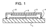
- Fig. 1 is a sectional schematic illustrative of one embodiment of the organic EL device of the invention. As illustrated in Fig. 1, this embodiment is built up of an organic EL structure 2 formed on a substrate 1 and a sealing sheet 3 that is located at such a given spacing that the organic EL structure 2 is covered therewith.
- the sealing sheet 3 is bonded and fixed by an adhesive agent 4 to the substrate 2 in such a way as to seal up the organic EL structure 2 therein.
- On the inside surface of the sealing sheet fixed by the adhesive agent 4 there is provided a mixture 5 of silicone resin with the drying agent.
- the sealing sheet may be made of transparent or translucent materials such as glasses, quartz, and resins, among which the glasses are preferred.
- a glass flat sheet By using a glass flat sheet, it is possible to achieve an inexpensive yet thin-film organic EL display device.
- alkali glass is preferable from a cost standpoint.
- Other preferable glass materials include soda lime glass, lead alkali glass, borosilicate glass, aluminosilicate glass, and silica glass.
- a soda glass material subjected to no surface treatment is inexpensive and, hence, preferable.
- a metal sheet, a plastic sheet, etc., too, may be used in place of the sealing glass sheet.
- the size of the sealing sheet is not critical to the present invention, and so may be properly determined depending on display area design, circuit design, etc.
- the sealing sheet when it is in a flat form, has a thickness of usually about 0.1 mm to about 5 mm. It is acceptable that the sealing sheet may be provided with a recess for receiving the whole or a part of the organic EL structure.
- a spacer is used to keep the sealing sheet at a height as desired.
- the spacer material may be resin beads, silica beads, glass beads, glass fibers, etc., with the glass beads being most preferred.
- the spacer is usually in a particulate form having a uniform particle size. In the invention, however, a spacer of any desired shape may be used provided that it can function well.
- the spacer size should preferably be 1 to 20 ⁇ m, more preferably 1 to 10 ⁇ m and even more preferably 2 to 8 ⁇ m, as calculated on a circle diameter basis.
- a spacer having such a diameter should preferably have a particle length of up to about 100 ⁇ m. Although there is no particular lower limit to the particle size, the particle size should usually be equal to or larger than the diameter.
- the spacer may or may not be used when a recess is provided in the sealing sheet.
- its size is preferably within the aforesaid range, and more preferably within the range of 2 to 8 ⁇ m.
- the spacer may have been incorporated in the sealing adhesive agent or may be incorporated in the sealing adhesive agent at the time of bonding.
- the content of the spacer in the sealing adhesive agent should be preferably 0.01 to 30 wt% and more preferably 0.1 to 5 wt%.
- thermosetting type adhesive agent it is preferable to use a photo-curing type adhesive agent in consideration of influences on the organic EL structure, although a thermosetting type adhesive agent may be used as well.
- a thermosetting type adhesive agent may be used as well.
- radical adhesive agents using various acrylate resins such as ester acrylate, urethane acrylate, epoxy acrylate, melamine acrylate and acrylic resin acrylate, and urethane polyester resin
- cationic adhesive agents using resins such as epoxy and vinyl ether
- thiol ⁇ en addition type resin adhesive agents preference is given to the cationic adhesive agent because there is no oxygenous obstacle and a polymerization reaction proceeds even after light irradiation.
- a preferred example of the cationic adhesive agent is a cation curing epoxy resin adhesive agent of the ultraviolet curing type.
- Each of the organic layers forming the organic EL structure has a glass transition temperature of usually 140°C or lower and especially about 80 to 100°C.
- an ordinary thermosetting type adhesive agent cannot be used with an organic EL device, because its setting temperature is of the order of 140 to 180°C; the organic EL structure is softened upon the setting of the adhesive agent, resulting in a deterioration in its performance.
- an ultraviolet curing type adhesive agent on the other hand, such a softening problem does not arise.
- a commonly used current ultraviolet curing type adhesive agent is an acrylic adhesive agent which is found to have an adverse influence on structural materials forming the organic EL structure because of the volatilization of the acrylic monomer contained therein during curing. As a consequence, the performance of the organic EL structure becomes worse.
- ultraviolet curing type epoxy resin adhesive agents include a combined ultraviolet and heat curing type epoxy resin adhesive agent.
- a radical curing type acrylic resin is often mixed or modified with a heat curing type epoxy resin.
- this adhesive agent is not preferable for use with the organic EL display of the present invention because the problem incidental to the volatilization of the acrylic monomer in the acrylic resin or the problem in connection with the setting temperature of the thermosetting type resin remains still unsolved.
- cation curing type ultraviolet curing epoxy resin adhesive agent used herein is intended an adhesive agent of the type which contains as a primary curing agent a Lewis acid-base type curing agent subjected to photo-decomposition upon ultraviolet or other light irradiation to release a Lewis acid catalyst, and in which the main component epoxy resin is polymerized and cured through a cation polymerization type reaction mechanism while a Lewis acid generated by light irradiation acts as a catalyst.
- the epoxy resin contained as the main component in the aforesaid adhesive agent includes an epoxidized olefin resin, an alicyclic epoxy resin and a novolak epoxy resin.
- the aforesaid curing agent for instance, includes a Lewis acid-base of aromatic diazonium, a Lewis acid-base of diallyliodonium, a Lewis acid-base of triallylsulfonium and a Lewis acid-base of triallylselenium, among which the Lewis acid-base of diallyliodonium is preferred.
- the amount of the adhesive agent to be coated is preferably 6 x 10 -2 to 2 x 10 -4 g/cm 2 and especially 8 x 10 -3 to 2 x 10 -4 g/cm 2 , although varying with the size of the organic EL structure stacked on the substrate or the type, structure and the like of a display built up of organic EL devices.
- the thickness of the adhesive agent layer should usually ensure that the predetermined space is available at the height at which the sealing sheet is located, i.e., in the thickness of the organic EL structure stacked on the substrate; it is of the order of usually 5 x 10 5 to 1 x 10 3 nm, preferably 5 x 10 4 to 5 x 10 3 nm and more preferably 2 x 10 4 to 2 x 10 3 nm, although the invention is not particularly limited thereto.
- the sealing sheet is bonded and sealed up.
- inert gases such as Ar, He and N 2 are preferred.
- the sealing gas should also preferably have a moisture content of 100 ppm or lower, preferably 10 ppm or lower and more preferably 1 ppm or lower. Usually but not exclusively, the lower limit to the moisture content is usually of the order of 0.1 ppm.
- the substrate material transparent or translucent materials such as glass, quartz and resin may be used when the emitted light is taken out of the substrate side.
- the substrate may be either transparent or opaque.
- the substrate, which it is opaque, may be formed of ceramics or the like.
- the substrate may be provided with a color filter film, fluorescent material-containing color conversion film or dielectric reflecting film for controlling the color of light emission.
- a color filter employed with liquid crystal display equipment may be used.
- an optical thin film such as a dielectric multilayer film may be used.
- the fluorescent color conversion film absorbs light emitted from an EL device and gives out light from the fluorescent substance contained therein for the color conversion of light emission, and is composed of three components, a binder, a fluorescent material and a light absorbing material.
- a fluorescent material having high fluorescent quantum efficiency and especially a fluorescent material having strong absorption in an EL light emission wavelength region.
- Laser dyes are suitable for the practice of the invention. To this end, for instance, it is prefezable to use rohodamine compounds, perylene compounds, cyanine compounds, phthalocyanine compounds (including subphthalocyanine compounds, etc.), naphthaloimide compounds, fused cyclic hydrocarbon compounds, fused heterocyclic compounds, styryl compounds and coumarin compounds.
- the binder it is basically preferable to make an appropriate selection from materials that do not extinguish fluorescence. It is particularly preferable to use a material that can be finely patterned by photolithography, printing or the like. It is also preferable to use a material that is not damaged during ITO or IZO film formation.
- the light absorbing material is used when light is not fully absorbed by the fluorescent material, and so may be dispensed with, if not required.
- the light absorbing material it is preferable to make a selection from materials that do not extinguish fluorescence.
- a transparent electrode For the hole injecting electrode, it is usually preferable to use a transparent electrode because the organic EL device is designed to take out the emitted light from the substrate side thereof.
- a transparent electrode for instance, include ITO (tin-doped indium oxide), IZO (zinc-doped indium oxide), ZnO, SnO 2 and In 2 O 3 , with ITO (tin-doped indium oxide) and IZO (zinc-doped indium oxide) being preferred.
- ITO tin-doped indium oxide
- IZO zinc-doped indium oxide
- ITO contains In 2 O 3 and SnO 2 in stoichiometric composition, although the amount of O may deviate sligthly from this.
- the hole injecting electrode may have at least a certain thickness enough for hole injection; that is, it may have a thickness of preferably 10 to 500 nm and more preferably 30 to 300 nm. There is no particular upper limit to the thickness. However, too thick a hole injecting electrode offers problems such as peeling, processability drops, defects by stresses, light transmittance drops and leakage by surface roughness. Too thin a hole injecting electrode offers problems in terms of as-fabricated film strength, hole transport capabilities and resistance values.
- the hole injecting electrode may be formed as by evaporation, but should preferably be formed by a sputtering technique.
- the electrode out of which light is taken should have a light transmittance of at least 50%, preferably at least 60%, more preferably at least 80% and even more preferably at least 90% at a light emission wavelength band of usually 400 to 700 nm, and especially with respect to each emitted light.
- a light transmittance of at least 50%, preferably at least 60%, more preferably at least 80% and even more preferably at least 90% at a light emission wavelength band of usually 400 to 700 nm, and especially with respect to each emitted light.
- the transmittance decreases, the light emitted from the light emitting layer attenuates in itself, and so it is difficult to obtain the luminance needed for the light emitting device. It is here noted that relatively low transmittance is often preferable for the purpose of improving contrast ratios, visibility, etc.
- the electron injecting electrode it is preferable to use a material having a low work function, e.g., any one of metal elements K, Li, Na, Mg, La, Ce, Ca, Sr, Ba, Al, Ag, In, Sn, Zn and Zr.
- a material having a low work function e.g., any one of metal elements K, Li, Na, Mg, La, Ce, Ca, Sr, Ba, Al, Ag, In, Sn, Zn and Zr.
- binary or ternary alloy systems containing metal elements Preferred alloy systems, for instance, are AgMg systems (Ag: 1 to 20 at%), Al ⁇ Li systems (Li: 0.3 to 14 at%), In ⁇ Mg systems (Mg: 50 to 80 at%) and Al ⁇ Ca system (Ca: 5 to 20 at%). It is acceptable to use these oxides in combination with an auxiliary electrode.
- the electron injecting electrode may be formed by evaporation, sputtering or the like.
- the thin film form of electron injecting electrode may have at least a certain thickness enough for the injection of electrons, e.g., of at least 0.1 nm and preferably at least 1 nm. Thus, a film thickness of the order of 1 to 500 nm is usually preferable although there is no upper limit thereto.
- a protective electrode may further be provided on the electron injecting electrode.
- the protective electrode may have at least a certain thickness enough to make sure of electron injection efficiency and prevent penetration of moisture, oxygen or organic solvents, for instance, of at least 50 nm, preferably at least 100 nm and especially 100 to 1,000 nm.
- a protective electrode layer With too thin a protective electrode layer, neither are the advantages of the invention obtainable, nor is sufficient connection with terminal electrodes obtainable because the ability of the protective electrode layer to cover steps becomes low.
- the protective electrode layer is too thick, on the other hand, the growth rate of dark spots becomes high because of an increase in the stress of the protective electrode layer.
- the total thickness of the electron injecting electrode plus the protective electrode is usually of the order of 100 to 1,000 nm.
- an additional protective film may be formed after the formation of the electrode.
- the protective film may be formed of either an inorganic material such as SiOx or an organic material such as Teflon, and a chlorine-containing carbon fluoride polymer.
- the protective film may be either transparent or opaque, and has a thickness of the order of 50 to 1,200 nm.
- the protective film may be formed either by the aforesaid reactive sputtering process or conventional processes such as general sputtering, evaporation or PECVD.
- the organic EL device of the present invention is generally of the DC or pulse drive type while it may be of the AC drive type.
- the applied voltage is generally of the order of 2 to 30 V.
- Liquid silicone rubber (KE109 made by the Shin-Etsu Chemical Co., Ltd.) was used as the resin compound and CaH 2 was used for the drying agent.
- the drying agent was mixed under agitation with the liquid silicone rubber in an amount of 100 parts by weight per 100 parts by weight of the main component of the liquid silicone rubber.
- a curing agent for the liquid silicone rubber was mixed under agitation with the mixture in an amount of 80 parts by weight per 100 parts by weight of the main component of the liquid silicone rubber, thereby obtaining a liquid silicone rubber/drying agent mixture.
- the obtained drying agent/silicone rubber mixture was coated on a portion of the sealing sheet forming an inside surface thereof (the side opposite to the organic EL structure) in an amount of about 0.05 g/cm 2 .
- Liquid silicone rubber (KE103 made by the Shin-Etsu Chemical Co., Ltd.) was used as the resin compound and CaH 2 was used for the drying agent.
- the drying agent was mixed under agitation with the liquid silicone rubber in an amount of 100 parts by weight per 80 parts by weight of the main component of the liquid silicone rubber.
- a curing agent for the liquid silicone rubber was mixed under agitation with the mixture in an amount of 80 parts by weight per 100 parts by weight of the main component of the liquid silicone rubber, thereby obtaining a liquid silicone rubber/drying agent mixture.
- the obtained drying agent/silicone rubber mixture was coated on a portion of the sealing sheet forming an inside surface thereof (the side opposite to the organic EL structure) in an amount of about 0.05 g/cm 2 .
- a 7059 substrate (trade name, Corning Co., Ltd.) as a glass substrate was scrubbed with neutral detergent.
- An ITO hole injecting electrode layer of 200 nm in thickness was formed on the substrate at a substrate temperature of 250°C by means of an RF magnetron sputtering process using an ITO oxide target.
- the substrate with the ITO electrode layer, etc. formed thereon was cleaned on its surface with UV/O 3 .
- the substrate was fixed to a substrate holder in a vacuum evaporation system, which was evacuated to a vacuum of 1 x 10 -4 Pa or lower.
- TPD N,N'-diphenyl-N,N'-m-tolyl-4,4'-diamino-1,1'-biphenyl
- N,N,N',N'-tetrakis(m-biphenyl)-1,1'-biphenyl-4,4'-diamine TPD
- rubrene tris(8-quinolinolato)aluminum
- TPD:Alq 3 mixture 1:1 (weight ratio) was doped with 10% by volume of rubrene.
- AlLi (Li: 7 at%) was deposited by evaporation to a thickness of 1 nm, and Al was subsequently deposited by evaporation to a thickness of 200 nm, thereby forming an electron injecting electrode and an auxiliary electrode.
- Each of the glass sheet sample Nos. 1 and 2 with the drying agent/resin mixture coated thereon was used to seal up the organic EL structure, thereby obtaining an organic EL device.
- the adhesive agent an epoxy type photo-curing adhesive agent was used.
- a comparative sample 1 was provided, in which a sealing sheet with no drying agent/resin mixture coated thereon was used.
- a panel sealed up with the drying agent/resin compound mixture coated on the sealing surface was treated at 85°C for 2 hours in an air atmosphere to cure the liquid silicone rubber and thermally treat the organic layers, thereby obtaining an organic EL device.
- comparative samples were also obtained by thermal treatment in a 100°C atmosphere (comparative sample No. 2) and in a 50°C atmosphere (comparative sample No. 3).
- each of ten such organic EL device samples was continuously driven at a current density of 10 mA/cm 2 under 60°C - RH 95% conditions. Five hundred hours later, the light emitting surface was observed to examine how many dark spots occurred per pixel. In the case of inventive sample Nos. 1 and 2, only about 3 dark spots of 50 mm or less in diameter were found. In the case of comparative sample No. 1, however, at least 20 dark spots, each having a diameter of at least 50 ⁇ m, were observed.
- an organic EL device which, in terms of deterioration with time such as the occurrence and spreading of dark spots, is reduced as much as possible so as to have an ever longer service life, an ever higher luminance, an ever higher efficiency and an ever high display quality.
Landscapes
- Electroluminescent Light Sources (AREA)
- Drying Of Gases (AREA)
- Solid-Sorbent Or Filter-Aiding Compositions (AREA)
Applications Claiming Priority (2)
| Application Number | Priority Date | Filing Date | Title |
|---|---|---|---|
| JP23365399 | 1999-08-20 | ||
| JP11233653A JP2001057287A (ja) | 1999-08-20 | 1999-08-20 | 有機el素子 |
Publications (2)
| Publication Number | Publication Date |
|---|---|
| EP1079666A2 true EP1079666A2 (de) | 2001-02-28 |
| EP1079666A3 EP1079666A3 (de) | 2002-01-09 |
Family
ID=16958428
Family Applications (1)
| Application Number | Title | Priority Date | Filing Date |
|---|---|---|---|
| EP00306544A Withdrawn EP1079666A3 (de) | 1999-08-20 | 2000-08-01 | Organische elektrolumineszente Vorrichtung |
Country Status (2)
| Country | Link |
|---|---|
| EP (1) | EP1079666A3 (de) |
| JP (1) | JP2001057287A (de) |
Cited By (15)
| Publication number | Priority date | Publication date | Assignee | Title |
|---|---|---|---|---|
| WO2003096751A1 (en) * | 2002-05-10 | 2003-11-20 | Koninklijke Philips Electronics N.V. | Electroluminescent panel |
| WO2003098973A1 (en) * | 2002-05-15 | 2003-11-27 | Koninklijke Philips Electronics N.V. | Method of manufacturing a flat panel display |
| WO2005050751A3 (en) * | 2003-11-12 | 2005-07-28 | Du Pont | Encapsulation assembly for electronic devices |
| EP1407818A4 (de) * | 2001-07-16 | 2005-11-16 | Nitto Denko Corp | Flächengebilde zur behandlung von gasförmigem bestandteil und elektrolumineszenzelement, bei dem dieses verwendet wird |
| US7178927B2 (en) | 2000-11-14 | 2007-02-20 | Semiconductor Energy Laboratory Co., Ltd. | Electroluminescent device having drying agent |
| US7692186B2 (en) | 2002-01-24 | 2010-04-06 | Semiconductor Energy Laboratory Co., Ltd. | Light emitting device and method of manufacturing the same |
| US7732060B2 (en) | 2000-03-31 | 2010-06-08 | Nitto Denko Corporation | Sheet for treating gaseous ingredient and electroluminescent element employing the same |
| US7820592B2 (en) | 2003-02-17 | 2010-10-26 | Saes Getters S.P.A. | Composition and devices for gas sorption and process for their manufacturing |
| US8383455B2 (en) | 2005-12-23 | 2013-02-26 | E I Du Pont De Nemours And Company | Electronic device including an organic active layer and process for forming the electronic device |
| US8680766B2 (en) | 2007-11-06 | 2014-03-25 | Japan Display Inc. | Organic electroluminescence display device and manufacturing method thereof |
| WO2014083110A1 (fr) * | 2012-11-29 | 2014-06-05 | Agc Glass Europe | Dispositif organique électronique ou optoélectronique laminé |
| US9583733B2 (en) | 2013-07-19 | 2017-02-28 | Panasonic Intellectual Property Management Co., Ltd. | Organic electroluminescent element and illumination device |
| USRE47311E1 (en) | 2005-01-03 | 2019-03-19 | Macronix International Co., Ltd. | Silicon on insulator and thin film transistor bandgap engineered split gate memory |
| CN110993813A (zh) * | 2019-11-14 | 2020-04-10 | 深圳市华星光电半导体显示技术有限公司 | Oled显示面板及其制备方法 |
| US11495776B2 (en) | 2018-04-16 | 2022-11-08 | Shin-Etsu Chemical Co., Ltd. | Transparent desiccant for organic EL, and method for using same |
Families Citing this family (10)
| Publication number | Priority date | Publication date | Assignee | Title |
|---|---|---|---|---|
| JP2002043055A (ja) * | 2000-05-17 | 2002-02-08 | Tohoku Pioneer Corp | 有機el素子及びその製造方法 |
| KR100756663B1 (ko) * | 2001-04-20 | 2007-09-07 | 엘지.필립스 엘시디 주식회사 | 유기전계발광소자의 패키징장치 |
| JP4627966B2 (ja) * | 2002-01-24 | 2011-02-09 | 株式会社半導体エネルギー研究所 | 発光装置およびその作製方法 |
| KR20040070976A (ko) * | 2003-02-05 | 2004-08-11 | 주식회사 엘리아테크 | 스티커형 봉지필름을 사용한 유기 전계발광 표시 패널 및그 제조방법 |
| WO2006013785A1 (ja) * | 2004-08-02 | 2006-02-09 | Dynic Corporation | 透明性乾燥剤 |
| JP4628210B2 (ja) * | 2004-08-02 | 2011-02-09 | ダイニック株式会社 | 透明性乾燥剤 |
| JP5232528B2 (ja) * | 2007-08-31 | 2013-07-10 | 富士フイルム株式会社 | 環境感受性デバイスの封止方法および画像表示素子 |
| JP5494648B2 (ja) * | 2009-03-13 | 2014-05-21 | コニカミノルタ株式会社 | 有機エレクトロニクス素子及びその製造方法 |
| KR20120078291A (ko) * | 2010-12-31 | 2012-07-10 | 제일모직주식회사 | 유기발광소자용 흡습충전재, 그 제조방법 및 이를 포함하는 유기발광소자 |
| JP6915527B2 (ja) * | 2017-12-27 | 2021-08-04 | 信越化学工業株式会社 | 有機el用透明乾燥剤及びその使用方法 |
Family Cites Families (9)
| Publication number | Priority date | Publication date | Assignee | Title |
|---|---|---|---|---|
| US4406839A (en) * | 1982-07-28 | 1983-09-27 | The B. F. Goodrich Company | Process for preparing organic solvent soluble amine molybdates |
| JPS63213289A (ja) * | 1987-02-28 | 1988-09-06 | アルプス電気株式会社 | 薄膜el素子 |
| JPH02197071A (ja) * | 1989-01-26 | 1990-08-03 | Sharp Corp | 薄膜elパネル |
| JPH01145085U (de) * | 1989-02-27 | 1989-10-05 | ||
| JPH02145085U (de) * | 1989-03-23 | 1990-12-10 | ||
| JPH09148066A (ja) * | 1995-11-24 | 1997-06-06 | Pioneer Electron Corp | 有機el素子 |
| JPH1140352A (ja) * | 1997-07-11 | 1999-02-12 | Tdk Corp | 有機el素子およびその製造方法 |
| JP2000003783A (ja) * | 1998-06-12 | 2000-01-07 | Tdk Corp | 有機el表示装置 |
| JP2000208252A (ja) * | 1999-01-14 | 2000-07-28 | Tdk Corp | 有機el素子 |
-
1999
- 1999-08-20 JP JP11233653A patent/JP2001057287A/ja active Pending
-
2000
- 2000-08-01 EP EP00306544A patent/EP1079666A3/de not_active Withdrawn
Cited By (23)
| Publication number | Priority date | Publication date | Assignee | Title |
|---|---|---|---|---|
| US7732060B2 (en) | 2000-03-31 | 2010-06-08 | Nitto Denko Corporation | Sheet for treating gaseous ingredient and electroluminescent element employing the same |
| US7178927B2 (en) | 2000-11-14 | 2007-02-20 | Semiconductor Energy Laboratory Co., Ltd. | Electroluminescent device having drying agent |
| US8557324B2 (en) | 2000-11-14 | 2013-10-15 | Semiconductor Energy Laboratory Co., Ltd. | Light emitting device |
| EP1407818A4 (de) * | 2001-07-16 | 2005-11-16 | Nitto Denko Corp | Flächengebilde zur behandlung von gasförmigem bestandteil und elektrolumineszenzelement, bei dem dieses verwendet wird |
| US8089066B2 (en) | 2002-01-24 | 2012-01-03 | Semiconductor Energy Laboratory Co., Ltd. | Light emitting device |
| US9627459B2 (en) | 2002-01-24 | 2017-04-18 | Semiconductor Energy Laboratory Co., Ltd. | Display device having sealing material |
| US9312323B2 (en) | 2002-01-24 | 2016-04-12 | Semiconductor Energy Laboratory Co., Ltd. | Light emitting device having insulator between pixel electrodes and auxiliary wiring in contact with the insulator |
| US8779467B2 (en) | 2002-01-24 | 2014-07-15 | Semiconductor Energy Laboratory Co., Ltd. | Light emitting device having a terminal portion |
| US7692186B2 (en) | 2002-01-24 | 2010-04-06 | Semiconductor Energy Laboratory Co., Ltd. | Light emitting device and method of manufacturing the same |
| US7459220B2 (en) | 2002-05-10 | 2008-12-02 | Koninklijke Philips Electronics, N.V. | Electroluminescent panel |
| WO2003096751A1 (en) * | 2002-05-10 | 2003-11-20 | Koninklijke Philips Electronics N.V. | Electroluminescent panel |
| WO2003098973A1 (en) * | 2002-05-15 | 2003-11-27 | Koninklijke Philips Electronics N.V. | Method of manufacturing a flat panel display |
| US7820592B2 (en) | 2003-02-17 | 2010-10-26 | Saes Getters S.P.A. | Composition and devices for gas sorption and process for their manufacturing |
| WO2005050751A3 (en) * | 2003-11-12 | 2005-07-28 | Du Pont | Encapsulation assembly for electronic devices |
| USRE47311E1 (en) | 2005-01-03 | 2019-03-19 | Macronix International Co., Ltd. | Silicon on insulator and thin film transistor bandgap engineered split gate memory |
| US8383455B2 (en) | 2005-12-23 | 2013-02-26 | E I Du Pont De Nemours And Company | Electronic device including an organic active layer and process for forming the electronic device |
| US8680766B2 (en) | 2007-11-06 | 2014-03-25 | Japan Display Inc. | Organic electroluminescence display device and manufacturing method thereof |
| US9806281B2 (en) | 2012-11-29 | 2017-10-31 | Agc Glass Europe | Laminated electronic or optoelectronic organic device |
| BE1024011B1 (fr) * | 2012-11-29 | 2017-10-27 | Agc Glass Europe | Dispositif organique électronique ou optoélectronique laminé |
| WO2014083110A1 (fr) * | 2012-11-29 | 2014-06-05 | Agc Glass Europe | Dispositif organique électronique ou optoélectronique laminé |
| US9583733B2 (en) | 2013-07-19 | 2017-02-28 | Panasonic Intellectual Property Management Co., Ltd. | Organic electroluminescent element and illumination device |
| US11495776B2 (en) | 2018-04-16 | 2022-11-08 | Shin-Etsu Chemical Co., Ltd. | Transparent desiccant for organic EL, and method for using same |
| CN110993813A (zh) * | 2019-11-14 | 2020-04-10 | 深圳市华星光电半导体显示技术有限公司 | Oled显示面板及其制备方法 |
Also Published As
| Publication number | Publication date |
|---|---|
| JP2001057287A (ja) | 2001-02-27 |
| EP1079666A3 (de) | 2002-01-09 |
Similar Documents
| Publication | Publication Date | Title |
|---|---|---|
| EP1079666A2 (de) | Organische elektrolumineszente Vorrichtung | |
| EP1021070A1 (de) | Organische elektrolumineszente Vorrichtung | |
| US6284342B1 (en) | Organic EL display assembly | |
| US6259204B1 (en) | Organic electroluminescent device | |
| US6399222B2 (en) | Organic electroluminescent device | |
| US6268071B1 (en) | Organic electroluminescent device | |
| US6316874B1 (en) | Organic electroluminescent device | |
| JP4246830B2 (ja) | 有機el素子 | |
| US6322910B1 (en) | Organic electroluminescent device | |
| JP3411864B2 (ja) | 有機el表示装置 | |
| US6166488A (en) | Organic electroluminescent device | |
| US6252246B1 (en) | Organic electroluminescent device | |
| EP1020938A2 (de) | Organische elektrolumineszente Vorrichtung | |
| US6303239B1 (en) | Organic electroluminescent device | |
| JP4255041B2 (ja) | 有機el素子 | |
| JP2000113976A (ja) | 有機el素子 | |
| EP1014757A2 (de) | Organische elektrolumineszente Vorrichtung | |
| EP1014758A2 (de) | Organische elektrolumineszente Vorrichtung | |
| EP0892587A2 (de) | Organische elektrolumineszente Vorrichtung und Verfahren zur Herstellung derselben | |
| US6262433B1 (en) | Organic electroluminescent device | |
| JP2000277254A (ja) | 有機el素子 | |
| JPH11121170A (ja) | 有機el素子およびその製造方法 | |
| JPH11176571A (ja) | 有機el素子の製造方法 | |
| JPH11195484A (ja) | 有機el素子 | |
| JPH11214152A (ja) | 有機el素子 |
Legal Events
| Date | Code | Title | Description |
|---|---|---|---|
| PUAI | Public reference made under article 153(3) epc to a published international application that has entered the european phase |
Free format text: ORIGINAL CODE: 0009012 |
|
| AK | Designated contracting states |
Kind code of ref document: A2 Designated state(s): AT BE CH CY DE DK ES FI FR GB GR IE IT LI LU MC NL PT SE |
|
| AX | Request for extension of the european patent |
Free format text: AL;LT;LV;MK;RO;SI |
|
| PUAL | Search report despatched |
Free format text: ORIGINAL CODE: 0009013 |
|
| AK | Designated contracting states |
Kind code of ref document: A3 Designated state(s): AT BE CH CY DE DK ES FI FR GB GR IE IT LI LU MC NL PT SE |
|
| AX | Request for extension of the european patent |
Free format text: AL;LT;LV;MK;RO;SI |
|
| RIC1 | Information provided on ipc code assigned before grant |
Free format text: 7H 05B 33/04 A, 7H 01L 51/20 B |
|
| AKX | Designation fees paid | ||
| REG | Reference to a national code |
Ref country code: DE Ref legal event code: 8566 |
|
| STAA | Information on the status of an ep patent application or granted ep patent |
Free format text: STATUS: THE APPLICATION IS DEEMED TO BE WITHDRAWN |
|
| 18D | Application deemed to be withdrawn |
Effective date: 20020710 |