EP1081937A2 - Bildverarbeitungsvorrichtung - Google Patents
Bildverarbeitungsvorrichtung Download PDFInfo
- Publication number
- EP1081937A2 EP1081937A2 EP00117835A EP00117835A EP1081937A2 EP 1081937 A2 EP1081937 A2 EP 1081937A2 EP 00117835 A EP00117835 A EP 00117835A EP 00117835 A EP00117835 A EP 00117835A EP 1081937 A2 EP1081937 A2 EP 1081937A2
- Authority
- EP
- European Patent Office
- Prior art keywords
- pixel
- interpolation
- compensation
- region
- interpolation point
- Prior art date
- Legal status (The legal status is an assumption and is not a legal conclusion. Google has not performed a legal analysis and makes no representation as to the accuracy of the status listed.)
- Granted
Links
Images





Classifications
-
- G—PHYSICS
- G06—COMPUTING OR CALCULATING; COUNTING
- G06T—IMAGE DATA PROCESSING OR GENERATION, IN GENERAL
- G06T3/00—Geometric image transformations in the plane of the image
- G06T3/40—Scaling of whole images or parts thereof, e.g. expanding or contracting
- G06T3/4015—Image demosaicing, e.g. colour filter arrays [CFA] or Bayer patterns
-
- H—ELECTRICITY
- H04—ELECTRIC COMMUNICATION TECHNIQUE
- H04N—PICTORIAL COMMUNICATION, e.g. TELEVISION
- H04N1/00—Scanning, transmission or reproduction of documents or the like, e.g. facsimile transmission; Details thereof
- H04N1/40—Picture signal circuits
Definitions
- the present invention relates to an image processing apparatus and, more particularly, to an image processing apparatus for generating a high-quality image from a two-dimensional color image signal sensed by such as a single-CCD color electronic camera device.
- an image having all color data (RGB or a luminance value and color difference signals) for each pixel is generated by interpolation processing of a pixel value for an image made up of many pixels arrayed in a matrix on a two-dimensional plane, each of which has the pixel value of only one of a plurality of colors (primary colors).
- the original image To display an image sensed by the image sensor on a display device smaller in the number of pixels than the image, the original image must be downsized. In this case, if pixels forming the original image are simply thinned out, data of the original image is omitted, so-called aliasing noise is generated, and resultant images are jaggy. Hence, to downsize an image, the original image must be sampled at an interval larger than the pixel interval of the original image after the high-frequency component of the original image is attenuated by a low-pass filter.
- an analog or digital low-pass filter and a re-sampling circuit may be conventionally arranged for each pixel line.
- filter calculation processing convolution calculation
- DSP Digital Signal Processor
- low-pass filter processing is done for each pixel of an intermediate image in units of a plurality of pixels contained in a predetermined region called a sub-matrix, and the sub-matrix is shifted on the original image while a portion overlapping a previous sub-matrix is left slightly.
- the conventional method must generate an intermediate image having all color data for each pixel of an original image before filter calculation processing. Even when a still image which need not be recorded is displayed, e.g., an image is displayed on the viewfinder of a digital still camera in order to determine the perspective, a large-size intermediate image having a large number of pixels is generated only to obtain a small-size image having a relatively small number of pixels for the viewfinder.
- the present invention has been made to overcome the conventional drawbacks, and has as its object to provide an image processing apparatus capable of obtaining a high-quality, small-size image at high speed without requiring a large number of processes or high power consumption.
- an image processing apparatus for generating, from an image signal, a new image signal having pixel values of all color data for each interpolation point set on a two-dimensional plane 1/n (n is an integer of not less than 2) times the image signal, comprising an interpolation unit for interpolating a pixel value of each color data at an interpolation point using pixel values of pixels of the same color falling within an interpolation region of m x m pixels (m is an integer of not less than 2) centered on the interpolation point, for an interpolation point selected at an interval of n pixels in at least a pixel line direction or a pixel column direction from an original image signal which has only a pixel value of single predetermined color data and is obtained by an image sensing element made up of many pixels that are arrayed in a matrix on a two-dimensional plane and respectively have different color filters, and for outputting the pixel value as an interpolated pixel value at the interpolation point for each color data
- Fig. 1 shows an image processing apparatus according to the first embodiment of the present invention.
- an image processing apparatus 10 comprises an interpolation unit 4 for interpolating the pixel value of each color data at an interpolation point using the pixel values of neighboring pixels of the same color positioned within an interpolation region of m x m pixels (m is an integer of 2 or more) centered on the interpolation point, with respect to an interpolation point selected from a two-dimensional plane constituted by an input image signal 1 at an interval of n pixels (n is an integer of 2 or more) in at least the pixel line direction or pixel column direction, and for outputting the interpolated value as an interpolated pixel value 5 at the interpolation point for each color data.
- the image processing apparatus 10 further comprises a compensation value calculation unit 6 for generating a pixel compensation value 7 for compensating for the pixel value of the interpolation point using the pixel values of a plurality of pixels around the interpolation point that fall within a compensation region of M x M pixels (M is an integer larger than n and m) wider than and including the interpolation region used by the interpolation unit 4, and a compensation unit 8 for compensating for the interpolated pixel value 5 of each color data at the interpolation point that is output from the interpolation unit 4 by using the pixel compensation value 7 obtained by the compensation value calculation unit 6, and for outputting the compensated value as a new pixel value 9 of each color data at the interpolation point.
- M is an integer larger than n and m
- the image signal 1 is an image signal output from an image sensing element such as a multi-color filtered CCD, i.e., an image signal having a so-called Bayer array in which R, G, and B pixels are arrayed in an almost checkered pattern.
- the image signal 1 is not limited to this.
- the present invention can be applied not only to a case wherein an image is reduced by 1/n from a two-dimensional plane formed from the input image signal 1 in either the pixel line direction or pixel column direction, but also to a case wherein an image is reduced by 1/n in both the pixel line direction and pixel column direction.
- Fig. 2A shows the two-dimensional plane image of an image signal
- Fig. 2B shows a setting example of each region
- Fig. 2C shows the two-dimensional plane image of a desired image signal.
- This also applies to a case wherein an image is downsized in only the pixel column direction and a case wherein an image is downsized in both the pixel line direction and pixel column direction.
- the interpolation unit 4 calculates the interpolated pixel value 5 at the interpolation point 11A using the pixel values of pixels contained in the interpolation region 12A.
- the compensation value calculation unit 6 calculates the pixel compensation value 7 at the interpolation point 11A using the pixel values of pixels contained in the compensation region 13A.
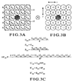
- Figs. 3A to 3C show a case wherein the interpolation point is set at an R pixel
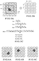
- Figs. 4A to 4C show a case wherein the interpolation point is set at a G pixel on an R pixel line.
- Fig. 3A shows a pixel array example
- Fig. 3B shows filter coefficients for calculating a compensation value
- Fig. 3C shows equations representing interpolation processing, compensation value calculation processing, and compensation processing.
- the interpolation unit 4 calculates the interpolated pixel values 5 (G 33 , R 33 , and B 33 ) at an interpolation point (X 33 ) set as the center by using the pixel values of predetermined pixels adjacent to the interpolation point X 33 among the pixels of the input image signal 1, as shown in Fig. 3A.
- Each interpolated pixel value 5 is calculated by the equation shown in Fig. 3C using the pixel values of peripheral pixels of the same color falling within an interpolation region 12 of 3 x 3 pixels which surrounds the interpolation point X 33 , i.e., is centered on the interpolation point X 33 .
- the compensation value calculation unit 6 generates the pixel compensation value 7 (HF 33 ) for compensating for the pixel value of each color data at the interpolation point by the equation shown in Fig. 3C using the pixel values of predetermined pixels around the interpolation point X 33 used by the interpolation unit 4, the filter coefficients shown in Fig. 3B, and a compensation scale factor (weighting factor) gf.
- Calculation of the pixel compensation value 7 uses predetermined pixels falling within a range, e.g., compensation region 13 of 5 x 5 pixels corresponding to the filter coefficients, that is wider than the interpolation region used for interpolation processing of the interpolation unit 4, and includes the interpolation region.
- the interpolated pixel value 5 calculated by the interpolation unit 4 does not contain any high spatial frequency component in the pixel region centered on the interpolation point.
- the pixel compensation value 7 contains a high spatial frequency component in the pixel region.
- the compensation unit 8 adds (or integrates) the pixel compensation value 7 to the interpolated pixel values 5, compensates for the interpolated pixel values 5 of respective color data, and calculates new pixel values 9 (G' 33 , R' 33 , and B' 33 ) of the respective color data at the interpolation point (X 33 ).
- Fig. 4A shows a pixel array example
- Fig. 4B shows filter coefficients for calculating a compensation value
- Fig. 4C shows equations representing interpolation processing, compensation value calculation processing, and compensation processing.
- the interpolation point is shifted by one pixel in the pixel line direction, compared to processing operation when the interpolation point is set at an R pixel, as shown in Figs. 3A to 3C.
- each interpolation point 11A is selected from the two-dimensional plane image 1A at an interval of n pixels in the pixel line direction i and pixel column direction j.
- the interpolation unit 4 calculates each interpolated pixel value 5 at the interpolation point 11A from the pixel values of pixels of the same color falling within the interpolation region 12A centered on the interpolation point 11A.
- the compensation value calculation unit 6 calculates the pixel compensation value 7 at the interpolation point 11A from the pixel values of a plurality of pixels falling within the compensation region 13A wider than and including the interpolation region 12A used by the interpolation unit 4.
- the compensation unit 8 compensates for each interpolated pixel value 5 using the pixel compensation value 7.
- a value which is omitted by interpolation using the interpolation region 12A in the interpolation unit 4 is compensated by the pixel compensation value 7 calculated from the compensation region 13A wider than and including the interpolation region 12A, thereby obtaining a new pixel value containing the high spatial frequency component.
- an intermediate image having all color data for each pixel of an original image need not be generated.
- a downsized image having all color data for each pixel can be attained with high image quality without performing a large number of processes.
- a high-quality image can be displayed at high speed without requiring high power consumption.
- the compensation value calculation unit 6 calculates the pixel compensation value 7 using only the pixel values of a plurality of pixels having color data which represents the luminance component of an image signal, e.g., using only the pixel values of G pixels for an image signal having a Bayer array, as shown in Figs. 3A to 3C and 4A to 4C.
- the compensation unit 8 can compensate for only luminance components for the pixel values of pixels of each color data without changing color balance.
- a pixel which represents a luminance component is the largest in number and has the highest frequency component, so that a new pixel value containing a higher frequency component can be obtained, compared to a pixel value interpolated by only pixels of the same color.
- Fig. 5A shows a pixel array example
- Fig. 5B shows filter coefficients for calculating a compensation value
- Fig. 5C shows equations representing interpolation processing, compensation value calculation processing, and compensation processing.
- the interpolation point is set at a pixel.
- the interpolation point is not limited to the same position as a pixel, and may be set at a position shifted from a pixel position, i.e., between pixels.
- an interpolation point a is set between pixels.
- the interpolation point a is set at a position shifted from the R pixel R 33 serving as the interpolation point X 33 in Fig. 3A to an upper right position and surrounded by four, R pixel R 33 , G pixel G 32 , G pixel G 43 , and B pixel B 42 .
- a compensation value calculation unit 6 generates a pixel compensation value 7 (HFa) for compensating for the pixel value of each color data at the interpolation point a by the equation shown in Fig. 5C using the pixel values of a plurality of pixels around the interpolation point a that fall within a range wider than and including the interpolation region used by the interpolation unit 4, the filter coefficients shown in Fig. 5B, and a compensation scale factor (weighting factor) gf.
- HFa pixel compensation value 7
- the interpolated pixel value 5 calculated by the interpolation unit 4 does not contain any high spatial frequency component in the pixel region centered on the interpolation point.
- the pixel compensation value 7 contains a high spatial frequency component corresponding to the pixel region and coefficients.
- a compensation unit 8 adds (or integrates) the pixel compensation value 7 to the interpolated pixel values 5, compensates for the interpolated pixel values 5 of the respective color data, and calculates new pixel values 9 (G'a, R'a, and B'a) of the respective color data at the interpolation point a .
- Figs. 6A to 6C show the setting position of the interpolation point.
- the interpolation point a is set at the upper right of the R pixel R 33 .
- the setting position of the interpolation point a may be set at the upper left, lower right, or lower left of the R pixel R 33 , as shown in Figs. 6A to 6C.
- the pixel array example in Fig. 5A is horizontally reversed (or rotated through 90°).
- the filter coefficients in Fig. 5B are horizontally reversed (or rotated through 90°).
- Figs. 6B and 6C R and B pixels in Figs. 5A and 6A are exchanged.
- the interpolated pixel values 5 are calculated by exchanging R and B.
- the interpolated pixel values 5 are calculated from pixels falling within the interpolation region of 2 x 2 pixels or 3 x 3 pixels including the interpolation point a
- the pixel compensation value 7 is calculated from predetermined pixels falling within the compensation region of 4 x 4 pixels wider than the interpolation region.
- the interpolation point is positioned at the upper right of an R pixel.
- a case wherein the interpolation point is positioned at the upper right of a G or B pixel corresponds to any one of the cases shown in Figs. 5A and 6A to 6C.
- the interpolation point a is set at the upper right of a G pixel on an R pixel line, the positional relationship between the target pixel and the interpolation point coincides with that in Fig. 6A. Processes for all cases can therefore be executed with the four patterns shown in Figs. 5A and 6A to 6C.
- the pixel compensation value 7 is calculated using only the pixel values of a plurality of pixels having color data which represents the luminance component of an image signal, e.g., using only the pixel values of G pixels for an image signal having a Bayer array. For this reason, the compensation unit 8 can compensate for only luminance components for the pixel values of pixels of each color data without changing color balance.
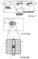
- Fig. 7 shows an image processing apparatus according to the third embodiment.
- the interpolation unit 4 and compensation value calculation unit 6 directly receive the image signal 1.
- a region value calculation unit 2 is adopted to receive and pre-process an image signal 1, and then the image signal 1 is distributed to an interpolation unit 4A and compensation value calculation unit 6A.
- the region value calculation unit 2 receives the image signal 1, and outputs the sums of the pixel values of pixels belonging to respective pixel regions, as region values 3 for the respective pixel regions set in advance on a sub-matrix made up of pixels to be processed including the interpolation point as the center.
- the region values 3 calculated by the region value calculation unit 2 are parallel-output in synchronism with reception of a pixel block.
- Processes executed in the interpolation unit 4A and compensation value calculation unit 6A are the same as in the interpolation unit 4 and compensation value calculation unit 6 in Fig. 1 except that the interpolation unit 4A and compensation value calculation unit 6A do not directly receive the image signal 1, but selectively use the region values 3 parallel-output from the region value calculation unit 2 to sequentially calculate and output interpolated pixel values 5 and a pixel compensation value 7 at the interpolation point on the corresponding sub-matrix.
- Figs. 8A and 8B show the basic operation in the third embodiment.
- Fig. 8A shows the two-dimensional plane image of an image signal
- Fig. 8B shows a setting example of each region.
- Figs. 9A to 9C show the operation of the region value calculation unit.
- Fig. 9A shows a compensation region
- Fig. 9B shows regions set in the compensation region
- Fig. 9C shows equations for calculating region values.
- the region value calculation unit 2 sequentially receives pixel values forming the image signal 1 by the number M of pixel lines (j direction), e.g., five pixel lines as the number of pixel lines necessary for calculating the pixel compensation value 7 in parallel with each other in units of single pixel columns as pixel blocks 21.
- a sub-matrix 22 equal in size to the compensation region is formed from the pixel blocks 21 corresponding to five pixel columns as M successively received pixel columns (i direction), e.g., the number of pixel columns necessary for calculating the pixel compensation value 7. Then, the sub-matrix 22 shifts by one pixel in the i direction on the two-dimensional plane image.
- the region value calculation unit 2 calculates the sums, i.e., region values 3 of the pixel values of pixels belonging the respective pixel regions on the basis of the equations in Fig. 9C. Then, the region value calculation unit 2 parallel-outputs the region values in synchronism with reception of the pixel block 21.
- the interpolation unit 4A and compensation value calculation unit 6A selectively use the parallel-output region values, and sequentially calculate and output interpolated pixel values and a pixel compensation value at the interpolation point on the corresponding sub-matrix.
- pixel regions are set based on equations used by the interpolation unit 4A and compensation value calculation unit 6A.
- Fig. 9B shows the pixel regions A to F when interpolation processing and pixel compensation value calculation processing in the first embodiment are employed. A case wherein the pixel regions A to F are set will be exemplified.
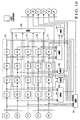
- Fig. 10 shows an arrangement of the region value calculation unit.
- reference numerals 121 to 125 denote shift registers each made up of four series-connected 1-pixel clock delays 211 to 214, 221 to 224, 231 to 234, 241 to 244, or 251 to 254.
- the shift registers 121 to 125 are arranged in parallel with each other for pixel values Vi1 to Vi5 of the pixel blocks 21.
- the "1-pixel clock delay" (to be referred to as a delay hereinafter) is a latch circuit for delaying and outputting an input pixel value in synchronism with a clock signal in the pixel line direction (i direction).
- the delays of the shift registers 121 to 125 output pixel values at pixel positions on the sub-matrix 22.
- adders 201 to 207 add all pixels belonging to the respective pixel regions and outputs from corresponding delays, thereby obtaining respective region values.
- the adder 201 adds outputs from the delays 221, 223, 241, and 243 corresponding to the region A in Fig. 9C to obtain a region value A.
- the region value calculation unit 2 calculates the region values 3 from the received sub-matrix 22, and parallel-outputs them.
- Fig. 11 shows an arrangement example of the interpolation unit and compensation value calculation unit.
- the interpolation unit 4A is constituted by R, B, and G interpolation units 41, 42, and 43 for performing interpolation processes concerning R, B, and G pixels, respectively.
- the interpolation units 41 to 43 parallel-calculate a plurality of interpolated pixel values corresponding to the position of the interpolation point using integrators (dividers) and adders.
- Corresponding interpolated pixel values are selected by selectors 41A to 43A based on O/E and R/B signals or only the O/E signal representing the position of an actual interpolation point, and output as interpolated pixel values 5 (R, B, and G) at the interpolation point.
- the R/B signal represents whether the interpolation point is on an R or B pixel line
- the O/E signal represents whether the interpolation point is at a G pixel.
- the compensation value calculation unit 6A also parallel-calculates a plurality of interpolated pixel values corresponding to the position of the interpolation point using integrators (dividers) and adders.
- a corresponding interpolated pixel value is selected by a selector 61 based on the O/E signal representing the position of an actual interpolation point, and output as a pixel compensation value 7 (HF) at the interpolation point.
- filter coefficients used to calculate a pixel compensation value coefficients which are the sums of powers of 2 and the sum of which is a power of 2 are used.
- the integrator (divider) used by the compensation value calculation unit 6A can be formed from a bit shift circuit, which greatly simplifies the circuit arrangement.
- Fig. 12 shows an arrangement of a compensation unit.
- reference numeral 81 denotes an integration unit made up of a plurality of integrators for integrating (dividing) the pixel compensation value 7 by a power value of 2. The respective integrators are parallel-connected.
- Reference numeral 82 denotes an adder for selectively adding at least one of outputs from the integrators of the integration unit 81 based on the compensation scale factor (weighting factor) gf.
- Reference numeral 84 denotes an adder for individually adding an output 83 from the adder 82 to the interpolated pixel values 5 (R, B, and G), and outputting the sums as new pixel values 9 (R', B', and C') at the interpolation point that are compensated with the pixel compensation value 7; and 85, a latch for holding outputs from the adder 84 in synchronism with the interpolated pixel position in accordance with a clock ⁇ n whose period corresponds to the interval of the interpolated pixel position, and outputting the new pixel values 9 forming an image 1/n times the input image signal 1.
- the interpolated pixel value 5 can be compensated by an intensity corresponding to gf.
- the integration unit 81 is constituted by a plurality of integrators for integrating power values of 2
- an arbitrary compensation scale factor gf can be integrated to the pixel compensation value 7 with a simple circuit arrangement. If the reference level of the pixel compensation value 7 changes in accordance with the position of the interpolation point, gf can be automatically switched in accordance with positional information of the interpolation point to adjust the reference level of the pixel compensation value 7.
- the third embodiment adopts the region value calculation unit 2.
- the region value calculation unit 2 calculates, as the region values 3 for respective pixel regions set in advance on the sub-matrix 22, the sums of the pixel values of pixels belonging to the respective pixel regions, and parallel-outputs the region values 3 in synchronism with reception of the pixel block 21.
- the interpolation unit 4A and compensation value calculation unit 6A selectively use the parallel-output region values, and sequentially calculate and output interpolated pixel values and a pixel compensation value at the interpolation point on the corresponding sub-matrix 22.
- the sub-matrix shifts on the two-dimensional plane image of the image signal 1 in synchronism with reception of the pixel block 21.
- a new interpolated pixel value compensated with the pixel compensation value 7 is attained as the interpolated pixel value of each color data at the interpolation point corresponding to the sub-matrix.
- the new interpolated pixel value is held and output in synchronism with an interpolated pixel selected from the input image signal 1 at an interval of n pixels in the pixel line direction and pixel column direction. This realizes pipeline processing synchronized with reception of the pixel block 21.
- An interpolated pixel value for a higher image quality can be calculated at a higher speed, compared to a case wherein interpolation processing is done by numerical calculation using a DSP or the like.
- the third embodiment has been described based on the first embodiment. Even based on the second embodiment, the third embodiment can attain the same effects as those described above by constituting the circuit in correspondence with the numbers of pixel lines and pixel columns necessary for compensation value calculation processing.
- the number of necessary pixels decreases, the number of latches for the buffer memory or delay decreases, and the necessary circuit area reduces.
- the decrease in the number of lines of data to be held in the buffer memory is very effective for an image sensing apparatus such as a recent digital still camera having a large number of pixels.
- the latch 85 is connected to the output of the adder 84.
- the latch 85 holds and outputs the outputs from the adder 84 in synchronism with an interpolated pixel selected from the input image signal 1 at an interval of n pixels in the pixel line direction and pixel column direction.
- the present invention is not limited to this.
- a latch for holding and outputting region values A to F based on the clock ⁇ n may be connected to the output of the region value calculation unit 2 (see Fig. 10)
- the new pixel values 9 can be obtained at an interval of n pixels.
- signals are output to circuits subsequent to the latch not every pixel but in units of n pixels.
- the processing operation speeds of these circuits can be set low, which reduces the power consumption.
- the power consumption amount can be reduced at maximum when latches are arranged at the input stages of the adders 201 to 207 of the region value calculation unit 2.
- pixel values not used for interpolation processing are reflected on compensated pixel values by not adding but subtracting a compensation value.
- an inverter 87 for inverting the polarity of an output 83 from an adder 82, and a selector 86 for selecting either one of an output from the inverter 87 and the output 83 from the adder 82 are arranged between the adder 82 and an adder 84.
- the selector 86 is controlled based on the comparison result of a comparator 88 for comparing m and n.
- the adder 84 adds a pixel compensation value 7 to an interpolated pixel value 5.
- n > m an input B to the selector 86 is selected as the output 89, and a signal prepared by inverting the output 83 from the adder 82 by the inverter 87 is output to the adder 84.
- the adder 84 subtracts the pixel compensation value 7 from the interpolated pixel value 5.
- pixel coefficients used for compensation are positive values, so that the same effects as those when a low-pass filter is applied to a compensation region can be obtained.
- the present invention adopts an interpolation unit for interpolating, for an interpolation point selected from an image signal at an interval of n pixels in the pixel line direction and pixel column direction, the pixel value of each color data at the interpolation point using the pixel values of pixels of the same color falling within an interpolation region of m x m pixels (m is an integer of 2 or more) centered on the interpolation point, and outputting the pixel value as an interpolated pixel value at the interpolation point for each color data, and a compensation value calculation unit for generating a pixel compensation value for compensating for the pixel value of the interpolation point using the pixel values of a plurality of pixels falling within a compensation region of M x M pixels (M is an integer equal to or larger than m and n) centered on the interpolation point that is wider than and includes the interpolation region.
- the interpolated pixel value of each color data at the interpolation point that is output from the interpolation unit is compensated using the pixel compensation value corresponding to the interpolation point that is obtained by the interpolation unit.
- the compensated pixel value is output as a new pixel value of each color data at the interpolation point.
- Interpolation processing using the pixels of the interpolation region and filter calculation processing for suppressing degradation of image quality caused by downsizing of an image can be executed at once. Unlike the prior art, an intermediate image having all color data for each pixel of an original image need not be generated. A downsized image having all color data for each pixel can be displayed at high speed with high image quality without requiring high power consumption.
Landscapes
- Engineering & Computer Science (AREA)
- Multimedia (AREA)
- Signal Processing (AREA)
- Physics & Mathematics (AREA)
- General Physics & Mathematics (AREA)
- Theoretical Computer Science (AREA)
- Image Processing (AREA)
- Color Television Image Signal Generators (AREA)
- Color Image Communication Systems (AREA)
Applications Claiming Priority (2)
| Application Number | Priority Date | Filing Date | Title |
|---|---|---|---|
| JP23355799A JP4361991B2 (ja) | 1999-08-20 | 1999-08-20 | 画像処理装置 |
| JP23355799 | 1999-08-20 |
Publications (3)
| Publication Number | Publication Date |
|---|---|
| EP1081937A2 true EP1081937A2 (de) | 2001-03-07 |
| EP1081937A3 EP1081937A3 (de) | 2003-11-19 |
| EP1081937B1 EP1081937B1 (de) | 2005-11-02 |
Family
ID=16956943
Family Applications (1)
| Application Number | Title | Priority Date | Filing Date |
|---|---|---|---|
| EP00117835A Expired - Lifetime EP1081937B1 (de) | 1999-08-20 | 2000-08-18 | Bildverarbeitungsvorrichtung zur Verringerung der Abtastfrequenz und zur Interpolation eines Bildsignals von einem Sensor mit Farbfilteranordnung |
Country Status (4)
| Country | Link |
|---|---|
| US (1) | US6654492B1 (de) |
| EP (1) | EP1081937B1 (de) |
| JP (1) | JP4361991B2 (de) |
| DE (1) | DE60023619T2 (de) |
Cited By (2)
| Publication number | Priority date | Publication date | Assignee | Title |
|---|---|---|---|---|
| WO2005055615A1 (en) * | 2003-12-05 | 2005-06-16 | Tandberg Telecom As | Improved calculation of interpolated pixel values |
| CN101867826A (zh) * | 2009-04-15 | 2010-10-20 | 佳能株式会社 | 图像处理设备和图像处理方法 |
Families Citing this family (15)
| Publication number | Priority date | Publication date | Assignee | Title |
|---|---|---|---|---|
| JP4065155B2 (ja) * | 2002-07-12 | 2008-03-19 | オリンパス株式会社 | 画像処理装置および画像処理プログラム |
| US7636095B2 (en) * | 2002-09-06 | 2009-12-22 | Ati Technologies, Inc. | Pixel delta interpolation method and apparatus |
| JP3942569B2 (ja) * | 2003-09-04 | 2007-07-11 | オリンパス株式会社 | 撮像装置および画像データの変換方法 |
| JP4128585B2 (ja) * | 2003-12-22 | 2008-07-30 | 三菱電機株式会社 | 画素信号処理装置及び画素信号処理方法 |
| US7502505B2 (en) | 2004-03-15 | 2009-03-10 | Microsoft Corporation | High-quality gradient-corrected linear interpolation for demosaicing of color images |
| US8165389B2 (en) * | 2004-03-15 | 2012-04-24 | Microsoft Corp. | Adaptive interpolation with artifact reduction of images |
| US7480417B2 (en) * | 2004-10-19 | 2009-01-20 | Microsoft Corp. | System and method for encoding mosaiced image data employing a reversible color transform |
| US7576783B2 (en) * | 2005-02-04 | 2009-08-18 | Hau Hwang | Confidence based weighting for color interpolation |
| JP4759293B2 (ja) * | 2005-03-15 | 2011-08-31 | キヤノン株式会社 | 撮像素子 |
| US8306362B2 (en) * | 2005-07-20 | 2012-11-06 | Omnivision Technologies, Inc. | Selective pixel binning and averaging based on scene illuminant |
| JP4735978B2 (ja) * | 2006-07-21 | 2011-07-27 | ソニー株式会社 | 画像処理装置、画像処理方法、及びプログラム |
| US20080123997A1 (en) * | 2006-11-29 | 2008-05-29 | Adams James E | Providing a desired resolution color image |
| US8594451B2 (en) * | 2007-03-30 | 2013-11-26 | Omnivision Technologies, Inc. | Edge mapping incorporating panchromatic pixels |
| CN101853488B (zh) * | 2010-06-03 | 2012-05-23 | 昆山龙腾光电有限公司 | 一种图像放大方法及装置 |
| JP2015201724A (ja) * | 2014-04-07 | 2015-11-12 | キヤノン株式会社 | 画像処理装置および画像処理方法 |
Family Cites Families (10)
| Publication number | Priority date | Publication date | Assignee | Title |
|---|---|---|---|---|
| US5323233A (en) * | 1990-07-31 | 1994-06-21 | Canon Kabushiki Kaisha | Image signal processing apparatus having a color filter with offset luminance filter elements |
| US5172227A (en) * | 1990-12-10 | 1992-12-15 | Eastman Kodak Company | Image compression with color interpolation for a single sensor image system |
| JPH04284087A (ja) * | 1991-03-13 | 1992-10-08 | Canon Inc | 電子スチルカメラ |
| US5481275A (en) * | 1992-11-02 | 1996-01-02 | The 3Do Company | Resolution enhancement for video display using multi-line interpolation |
| JP2931520B2 (ja) * | 1993-08-31 | 1999-08-09 | 三洋電機株式会社 | 単板式カラービデオカメラの色分離回路 |
| US5574572A (en) | 1994-09-07 | 1996-11-12 | Harris Corporation | Video scaling method and device |
| JP3164481B2 (ja) * | 1994-12-20 | 2001-05-08 | シャープ株式会社 | 撮像装置 |
| JP3392564B2 (ja) * | 1995-02-27 | 2003-03-31 | 三洋電機株式会社 | 単板式カラービデオカメラ |
| US6266373B1 (en) * | 1998-06-15 | 2001-07-24 | U.S. Philips Corporation | Pixel data storage system for use in half-pel interpolation |
| JP4317619B2 (ja) * | 1999-07-22 | 2009-08-19 | メディア・テック・ユーエスエイ・インコーポレーテッド | 画像処理装置 |
-
1999
- 1999-08-20 JP JP23355799A patent/JP4361991B2/ja not_active Expired - Lifetime
-
2000
- 2000-08-14 US US09/639,512 patent/US6654492B1/en not_active Expired - Lifetime
- 2000-08-18 EP EP00117835A patent/EP1081937B1/de not_active Expired - Lifetime
- 2000-08-18 DE DE60023619T patent/DE60023619T2/de not_active Expired - Fee Related
Cited By (3)
| Publication number | Priority date | Publication date | Assignee | Title |
|---|---|---|---|---|
| WO2005055615A1 (en) * | 2003-12-05 | 2005-06-16 | Tandberg Telecom As | Improved calculation of interpolated pixel values |
| US7616689B2 (en) | 2003-12-05 | 2009-11-10 | Tandberg Telecom As | Calculation of interpolated pixel values |
| CN101867826A (zh) * | 2009-04-15 | 2010-10-20 | 佳能株式会社 | 图像处理设备和图像处理方法 |
Also Published As
| Publication number | Publication date |
|---|---|
| JP2001086522A (ja) | 2001-03-30 |
| EP1081937B1 (de) | 2005-11-02 |
| DE60023619T2 (de) | 2006-08-10 |
| US6654492B1 (en) | 2003-11-25 |
| JP4361991B2 (ja) | 2009-11-11 |
| EP1081937A3 (de) | 2003-11-19 |
| DE60023619D1 (de) | 2005-12-08 |
Similar Documents
| Publication | Publication Date | Title |
|---|---|---|
| US6654492B1 (en) | Image processing apparatus | |
| EP1079604B1 (de) | Bildverarbeitungsgerät | |
| JP3190220B2 (ja) | 撮像装置 | |
| EP0641508B1 (de) | Methode und Vorrichtung zur Verbesserung der Schärfe einer einem kontinuierlichem Zoom unterworfenen Bildfolge | |
| KR100396898B1 (ko) | 이미지센서 출력데이터 처리장치 및 처리방법 | |
| KR100505681B1 (ko) | 베이어 패턴 컬러 신호에 대한 적응형 필터로 보간을수행하여 해상도를 높이는 보간기, 이를 구비한 디지털영상 신호 처리 장치, 및 그 방법 | |
| US4674125A (en) | Real-time hierarchal pyramid signal processing apparatus | |
| US5319451A (en) | Color signal processing apparatus using a common low pass filter for the luminance signal and the color signals | |
| US7499089B2 (en) | Color interpolation method in bayer array | |
| JP4350706B2 (ja) | 画像処理装置及び画像処理プログラム | |
| JP2002237998A (ja) | 画面補正方法及び撮像装置 | |
| US8154636B2 (en) | Image enhancement using hardware-based deconvolution | |
| EP1083753A2 (de) | Bildverarbeitungsvorrichtung | |
| US6701024B1 (en) | Image processing apparatus | |
| US5862268A (en) | Bilinear decimator with error compensation | |
| JP4133283B2 (ja) | 画像処理装置および画像処理方法、デジタルスチルカメラ | |
| EP1052845A2 (de) | Bildverarbeitungsvorrichtung | |
| CN103154999B (zh) | 图像信号处理装置、图像信号处理方法 | |
| JPH0715734A (ja) | 固体撮像素子の信号処理回路 | |
| US7149364B2 (en) | Mean filter device and filtering method | |
| EP0970582B1 (de) | Bilinearer dezimator mit fehlerkompensation | |
| KR100656644B1 (ko) | 영상압축에서의 움직임 보상을 위한 화면간 보간장치 | |
| JPH0993486A (ja) | ディジタル画像処理装置 | |
| JPH08279949A (ja) | 電子ズーム処理装置および電子ズーム処理方法 | |
| KR100459390B1 (ko) | 디지털스틸카메라의데시메이션회로 |
Legal Events
| Date | Code | Title | Description |
|---|---|---|---|
| PUAI | Public reference made under article 153(3) epc to a published international application that has entered the european phase |
Free format text: ORIGINAL CODE: 0009012 |
|
| AK | Designated contracting states |
Kind code of ref document: A2 Designated state(s): AT BE CH CY DE DK ES FI FR GB GR IE IT LI LU MC NL PT SE |
|
| AX | Request for extension of the european patent |
Free format text: AL;LT;LV;MK;RO;SI |
|
| PUAL | Search report despatched |
Free format text: ORIGINAL CODE: 0009013 |
|
| AK | Designated contracting states |
Kind code of ref document: A3 Designated state(s): AT BE CH CY DE DK ES FI FR GB GR IE IT LI LU MC NL PT SE |
|
| AX | Request for extension of the european patent |
Extension state: AL LT LV MK RO SI |
|
| RIC1 | Information provided on ipc code assigned before grant |
Ipc: 7H 04N 1/56 B Ipc: 7H 04N 9/04 B Ipc: 7H 04N 1/40 A |
|
| 17P | Request for examination filed |
Effective date: 20040428 |
|
| 17Q | First examination report despatched |
Effective date: 20040621 |
|
| AKX | Designation fees paid |
Designated state(s): DE FR GB IT NL |
|
| GRAP | Despatch of communication of intention to grant a patent |
Free format text: ORIGINAL CODE: EPIDOSNIGR1 |
|
| RTI1 | Title (correction) |
Free format text: IMAGE PROCESSING APPARATUS FOR DOWNSAMPLING AND INTERPOLATING AN IMAGE SIGNAL FROM A COLOUR FILTER ARRAY SENSOR |
|
| GRAS | Grant fee paid |
Free format text: ORIGINAL CODE: EPIDOSNIGR3 |
|
| GRAL | Information related to payment of fee for publishing/printing deleted |
Free format text: ORIGINAL CODE: EPIDOSDIGR3 |
|
| GRAS | Grant fee paid |
Free format text: ORIGINAL CODE: EPIDOSNIGR3 |
|
| GRAA | (expected) grant |
Free format text: ORIGINAL CODE: 0009210 |
|
| AK | Designated contracting states |
Kind code of ref document: B1 Designated state(s): DE FR GB IT NL |
|
| REG | Reference to a national code |
Ref country code: GB Ref legal event code: FG4D |
|
| REF | Corresponds to: |
Ref document number: 60023619 Country of ref document: DE Date of ref document: 20051208 Kind code of ref document: P |
|
| ET | Fr: translation filed | ||
| PGFP | Annual fee paid to national office [announced via postgrant information from national office to epo] |
Ref country code: FR Payment date: 20060822 Year of fee payment: 7 |
|
| PGFP | Annual fee paid to national office [announced via postgrant information from national office to epo] |
Ref country code: IT Payment date: 20060831 Year of fee payment: 7 |
|
| PLBE | No opposition filed within time limit |
Free format text: ORIGINAL CODE: 0009261 |
|
| STAA | Information on the status of an ep patent application or granted ep patent |
Free format text: STATUS: NO OPPOSITION FILED WITHIN TIME LIMIT |
|
| 26N | No opposition filed |
Effective date: 20060803 |
|
| PG25 | Lapsed in a contracting state [announced via postgrant information from national office to epo] |
Ref country code: NL Free format text: LAPSE BECAUSE OF NON-PAYMENT OF DUE FEES Effective date: 20070301 Ref country code: DE Free format text: LAPSE BECAUSE OF NON-PAYMENT OF DUE FEES Effective date: 20070301 |
|
| GBPC | Gb: european patent ceased through non-payment of renewal fee |
Effective date: 20060818 |
|
| NLV4 | Nl: lapsed or anulled due to non-payment of the annual fee |
Effective date: 20070301 |
|
| PG25 | Lapsed in a contracting state [announced via postgrant information from national office to epo] |
Ref country code: GB Free format text: LAPSE BECAUSE OF NON-PAYMENT OF DUE FEES Effective date: 20060818 |
|
| REG | Reference to a national code |
Ref country code: FR Ref legal event code: ST Effective date: 20080430 |
|
| PG25 | Lapsed in a contracting state [announced via postgrant information from national office to epo] |
Ref country code: FR Free format text: LAPSE BECAUSE OF NON-PAYMENT OF DUE FEES Effective date: 20070831 |
|
| PG25 | Lapsed in a contracting state [announced via postgrant information from national office to epo] |
Ref country code: IT Free format text: LAPSE BECAUSE OF NON-PAYMENT OF DUE FEES Effective date: 20070818 |