EP1083424A2 - Partikel-Erkennung und optisches System um die Substrat-Produktion zu erhöhen - Google Patents
Partikel-Erkennung und optisches System um die Substrat-Produktion zu erhöhen Download PDFInfo
- Publication number
- EP1083424A2 EP1083424A2 EP00307704A EP00307704A EP1083424A2 EP 1083424 A2 EP1083424 A2 EP 1083424A2 EP 00307704 A EP00307704 A EP 00307704A EP 00307704 A EP00307704 A EP 00307704A EP 1083424 A2 EP1083424 A2 EP 1083424A2
- Authority
- EP
- European Patent Office
- Prior art keywords
- substrate
- information
- chamber
- signal
- support member
- Prior art date
- Legal status (The legal status is an assumption and is not a legal conclusion. Google has not performed a legal analysis and makes no representation as to the accuracy of the status listed.)
- Withdrawn
Links
Images


Classifications
-
- G—PHYSICS
- G01—MEASURING; TESTING
- G01N—INVESTIGATING OR ANALYSING MATERIALS BY DETERMINING THEIR CHEMICAL OR PHYSICAL PROPERTIES
- G01N21/00—Investigating or analysing materials by the use of optical means, i.e. using sub-millimetre waves, infrared, visible or ultraviolet light
- G01N21/84—Systems specially adapted for particular applications
- G01N21/88—Investigating the presence of flaws or contamination
- G01N21/95—Investigating the presence of flaws or contamination characterised by the material or shape of the object to be examined
- G01N21/956—Inspecting patterns on the surface of objects
-
- H—ELECTRICITY
- H10—SEMICONDUCTOR DEVICES; ELECTRIC SOLID-STATE DEVICES NOT OTHERWISE PROVIDED FOR
- H10P—GENERIC PROCESSES OR APPARATUS FOR THE MANUFACTURE OR TREATMENT OF DEVICES COVERED BY CLASS H10
- H10P74/00—Testing or measuring during manufacture or treatment of wafers, substrates or devices
-
- G—PHYSICS
- G01—MEASURING; TESTING
- G01N—INVESTIGATING OR ANALYSING MATERIALS BY DETERMINING THEIR CHEMICAL OR PHYSICAL PROPERTIES
- G01N21/00—Investigating or analysing materials by the use of optical means, i.e. using sub-millimetre waves, infrared, visible or ultraviolet light
- G01N21/84—Systems specially adapted for particular applications
- G01N21/88—Investigating the presence of flaws or contamination
- G01N21/94—Investigating contamination, e.g. dust
-
- G—PHYSICS
- G01—MEASURING; TESTING
- G01N—INVESTIGATING OR ANALYSING MATERIALS BY DETERMINING THEIR CHEMICAL OR PHYSICAL PROPERTIES
- G01N21/00—Investigating or analysing materials by the use of optical means, i.e. using sub-millimetre waves, infrared, visible or ultraviolet light
- G01N21/84—Systems specially adapted for particular applications
- G01N21/88—Investigating the presence of flaws or contamination
- G01N21/95—Investigating the presence of flaws or contamination characterised by the material or shape of the object to be examined
- G01N21/9501—Semiconductor wafers
Definitions
- the present invention relates to a method and apparatus for detecting the presence of defects, such as particles on a substrate surface. More particularly, the invention utilizes a combination of a light source and a detector to illuminate a substrate surface and detect scattered energy therefrom.
- Semiconductor processing generally involves the deposition of material onto and removal ("etching") of material from substrates.
- Typical processes include chemical vapor deposition (CVD), physical vapor deposition (PVD), etching and others.
- CVD chemical vapor deposition
- PVD physical vapor deposition
- etching etching
- Sources of contamination include wear from mechanical motion, degradation of seals, contaminated gases, other contaminated substrates, flaking of deposits from processing chambers, nucleation of reactive gases, condensation during chamber pumpdown, arcing in plasma chambers and so forth.
- current semiconductor manufacturing routinely includes inspection of substrates for particles to identify "dirty" processes or equipment.
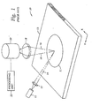
- FIG. 1 is a perspective view of an exemplary inspection apparatus 10.
- a substrate 11 is positioned on a stage 13 capable of moving in an X-Y plane.
- the stage 13 is also capable of rotation about an axis.
- a light source 12 emits light beam 14 onto the substrate 11 and irradiates the surface.
- the light beam 14 is focused as a spot by condenser lens 15 to define an inspected area of the substrate 11.
- Particles, device patterns, and other protrusions on the upper surface of the substrate 11 cause the incident light beam 14 to scatter in various directions, as shown by arrows 16, according to the light incidence angle and geometry of the protrusions.
- the scattered light 16 is received by a collector lens 18 and then transmitted to a detector 20 positioned in proximity to the substrate 11.
- the detector 20 is typically a Photo-Multiplier Tube (PMT), a charge-coupled device (CCD) or other light sensitive detector.
- the detector 20 converts the scattered light 16 into a signal corresponding to the detected protrusions on the substrate surface.
- the signal is routed to a processing unit 22 to generate data regarding various parameters of interest such as the size and location of the detected protrusions.
- Dark Field Illumination implies that only light scattered by protrusions on the substrate surface is detected and light which is merely reflected by the planar substrate surface is disregarded.
- the slit dimensions are adjusted to accommodate the width of the object under inspection so that the object need only be scanned in a single direction once.
- the light source is positioned to obliquely irradiate the reticle, thereby producing a non-uniform spot pattern.
- the light source is offset to one side of the reticle such that the reticle moves past the light source during a scan as opposed to toward or away from the light source. As a result, the light produces a more intense pattern on the portion of the reticle closer to the light source while a less intense pattern is produced farther away from the light source.
- the preferred inspection apparatus should be capable of being retrofitted to existing processing systems.
- the inspection apparatus should be positioned to allow inspection of each substrate before and/or after processing. Impact to throughput should be minimized by inspecting substrates "on-the-fly" during transfer between typical processing steps without the need for a separate inspection platform and stage.
- Another problem with particle detection systems is the noise produced by chip patterns formed on substrates.
- the patterns act as micro-mirrors causing the light to reflect in various directions.
- the patterns may produce misleading information, i.e. , the patterns may indicate the presence of foreign particles where none are found.
- various methods and apparatus have been implemented in the art.
- U.S. Pat. No. 5,463,419 entitled “Method and Apparatus for Analyzing the State of Generation of Foreign Particles in Semiconductor Fabrication Process," provides a method of detecting foreign particles on a substrate by "eliminating" the patterns formed on the substrate. For example, corresponding portions of adjacent chips are compared to determine differences. The chips are illununated with a light source to cause reflection of the light which is detected by detection equipment while the substrate is actuated by a conventional stage. The reflected distribution of light is then compared to determine the presence of foreign particles on the substrate. The portion of the resulting signals which are identical are erased leaving only differences in the signals. The differences are assumed to be the result of particles on the substrate.
- a preferred detection system would allow a quick decision to be made about whether an additional and more precise particle detection analysis is necessary.
- the system would also allow the substrate inspection to be performed on-the-fly and produce real-time data on each substrate undergoing processing, rather than just arbitrarily selected substrates from a batch.
- Such a preferred system would maximize the system throughput and reduce operating costs by eliminating the need for time-consuming inspection of small-scale particles and also the cost associated therewith.
- the present invention generally provides a particle detection apparatus in a processing system.
- a transmitter unit and a receiver unit are disposed on or near a chamber and cooperate to transmit and detect energy.
- the transmitter unit is positioned to transmit a signal onto a moving substrate surface.
- the receiver unit is positioned to collect a scattered portion of the signal and direct the same to a processing unit.
- a transmitter unit and a receiver unit are disposed on a semiconductor processing system and cooperate to transmit and detect energy, respectively.
- the transmitter unit is positioned to transmit a signal into a region of the processing system, such as a transfer chamber, and onto a substrate surface moving therethrough.
- the signal is transmitted onto a substrate moving through a cavity of the transfer chamber and preferably between the transfer chamber and an adjacent vacuum chamber.
- a robot preferably located in the transfer chamber or a front-end environment of the processing system, enables movement of the substrate.
- the receiver unit is disposed to collect a scattered portion of the signal and direct the same to a processing unit.
- the transmitter unit and the receiver unit are disposed in a region external to the processing system.
- a light source and one or more charge-coupled devices are disposed on or near a chamber and cooperate to transmit and detect energy, respectively.
- the laser source is positioned to transmit a signal onto a moving substrate surface.
- the CCD is disposed to collect a scattered portion of the signal and direct the signal to a processing unit.
- a signal is transmitted on a substrate moving in a first direction between a first vacuum chamber and a second vacuum chamber of a semiconductor processing system or rotationally within the first chamber.
- the first vacuum chamber is one of a transfer chamber or a front-end environment and the second vacuum chamber is one of a process chamber, a service chamber or a load lock chamber.
- a reflected portion of the signal is received by a receiver unit and subsequently directed to a processing unit for processing.
- the reflected portion of the signal is reflected by particles disposed on the substrate.
- the reflected portion of the signal is reflected by alphanumeric characters disposed on the substrate.
- a signal is transmitted on a substrate moving in a first direction between a first and second vacuum chamber of a semiconductor processing system or rotationally within the first chamber.
- the first vacuum chamber is one of a transfer chamber or a front-end environment and the second vacuum chamber is one of a process chamber, a service chamber or a load lock chamber.
- a reflected portion of the signal is received by a receiver unit and subsequently directed to a processing unit for processing.
- the processing unit is adapted to read a computer-readable program product to generate information pertaining to the substrate.
- the program product is adapted to provide substrate positional information, substrate reflectivity information, specular information, substrate defect information, substrate damage information, particle contamination information for the substrate support member and a substrate disposed thereon, alphanumeric character information, robot behavior information, calibration information for a robot, a transmitter unit and/or a receiver unit, and any combination thereof.
- a method of determining the center and/or orientation of a substrate is provided.
- a substrate is positioned in a chamber having a receiver unit and transmitter unit disposed therein.
- the surface of the substrate is illuminated with radiation from the transmitter unit and an image representative of at least an edge portion of the substrate is captured by the receiver unit.
- the image is analyzed to determine at least one of the center or orientation of the substrate.
- the substrate surface illuminated may be the backside of the substrate or the upper surface of the substrate in facing relation to the receiver unit.
- Figure 11 is perspective view of a prior art inspection apparatus.
- Figure 2 is a partial perspective view of a processing system.
- Figures 3A-C are top views of the processing system of Figure 2 showing various positions of a substrate disposed on a blade during rotation of the blade.
- Figure 4 is a top view of the processing system of Figure 2 showing a substrate disposed on a blade during retraction of the blade.
- Figure 5 is a plan view of a typical cluster tool for semiconductor processing.
- Figure 6 is a graphical representation of specular reflections on a patterned substrate illuminated by a light source.
- Figure 7 is a comparative graphical representation of specular reflections on patterned substrates.
- the present invention generally provides a particle detection apparatus in a processing system.
- a transmitter unit and a receiver unit are disposed on or near a chamber and cooperate to transmit and detect energy.
- the transmitter unit is positioned to transmit a signal onto a substrate surface moving between vacuum chambers. Particles disposed on the substrate surface cause a scattering of a portion of the signal.
- the receiver unit is positioned to collect and measure the scattered portion of the signal and direct the same to a processing unit.
- the transmitter unit comprises a light source and the receiver unit comprises a charged-coupled device (CCD).
- CCD charged-coupled device
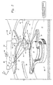
- FIG 2 is a perspective cutaway of a processing system 40 of the present invention comprising a transfer chamber 42 and a vacuum chamber 44 mounted thereon (see Fig. 3A).
- the transfer chamber 42 and the vacuum chamber 44 are selectively communicable through an aperture 46 which can be sealed by a conventional apparatus such as a slit valve door (not shown).
- the aperture 46 is sized to accommodate the transfer of substrates therethrough.
- a robot 50 is centrally disposed in the transfer chamber 42 and comprises a blade 48 coupled to the robot hub 51 by frog-leg type linkage 39. The robot 50 enables rotational and radial movement of the blade 48 along a transfer plane, thereby shuttling substrates between various positions.
- the transfer chamber 42 and the vacuum chamber 44 are preferably components of a cluster tool 100 such as the one shown in Figure 5 and described in detail below.
- the vacuum chamber 44 may be a load lock chamber providing an interfacing chamber between a front-end environment and the transfer chamber 42, while the transfer chamber 42 provides a vacuum environment communicable with various peripheral chambers.
- the vacuum chamber 44 may be a process chamber.
- a transmitter unit 56 and a receiver unit 58 are externally mounted to a lid 52 of the transfer chamber 42.
- the transmitter unit 56 includes a light source 60 and beam-shaping optics 62 and is positioned to emit a signal 54 into the cavity 41 of the transfer chamber 42 via a view port 64.
- the view port 64 comprises an opening formed in the lid 52 and is hermetically sealed with plate 66 made of a material transparent to the signal 54 of the light source 60.
- the plate 66 may comprise PyrexTM, for example.
- the signal 54 propagates parallel to the x-axis shown in Figure 2 and is directed onto an upper surface of a substrate 37 rotating through the cavity 41 of the transfer chamber 42.
- the signal defines a light pattern 53 upon falling on the substrate 37.
- the spot size of the light pattern 53 may be varied according the substrate size by adjusting the beam shaping optics 62 and the position of the light source 60.
- the light source 60 can be, for example, a laser source or a broad spectrum light source. In general, the light source 60 is selected according scattering intensity, brightness and cost. Where a laser source is used, the laser source is preferably operable at about 808nm. However, other laser sources, such as 650nm or 680nm wavelength laser sources, may also be used.
- the spot size of the light pattern 53 is substantially determined by the beam-shaping optics 62 and the position of the transmitter unit 56.
- the beam-shaping optics 62 is selected to provide a spot size according to the dimensions of the substrate.
- the spot size of the light pattern 53 is preferably at least 220 ⁇ m (width) x 300 mm (length, y-axis) on the upper surface of a substrate.
- Typical sources of catastrophic process chamber contamination such as flaking (also known as chamber excursions), provide hundreds of particles that may settle on the processing surface of a substrate.
- Successful particle detection requires only that a portion of the contaminants be detected to confirm the presence of a contaminated substrate.
- monitoring at least 60% of the processing surface ensures a substantial probability of detecting a contaminated substrate.
- the receiver unit 58 is shown mounted in a view port 70 formed in the lid 52 and defines an optical path 61 toward the substrate 37 moving through the cavity 41.
- the receiver unit 58 is secured above an energy transparent plate 72 made of a material selected according to the operating wavelength of the signal 54 and preferably comprises of the same material as the plate 66 disposed in view port 64.
- the material for the plates 66, 72 is selected to accommodate a 808nm signal.
- the receiver unit 58 is positioned to receive a scattered portion 74 of the signal 54 from the substrate 37 during operation.
- the scattered portion 64 is represented by a multiplicity of arrows oriented at various angles relative to the upper surface of the substrate 37 and indicates the presence of an obstruction, such as particulate contamination disposed on the upper surface of the substrate 37.
- a reflected portion 69 of the signal 54 propagates at angle relative to the substrate 37 substantially equal to the angle of incidence ⁇ .
- the reflected portion 69 represents the portion of the signal 54 substantially unobstructed upon intercepting the upper surface of the substrate 37.
- the receiver unit 58 includes an optics assembly 80, comprising one or more lens, and a detector 82.
- the detector 82 of the receiver unit 58 preferably comprises a charge-coupled device (CCD) line camera.
- CCD line camera is a preferred detector due to its high immunity to out-of-substrate noise and its ability to provide particle coordinates on a substrate. By using a line CCD the vertical coordinate of each detected particle can be determined.
- CCD detectors are preferred, other detectors, including time delay integration (TDI) detectors, or PMT's may be used to advantage. Where a TDI detector is used the spot is adjusted to correspond to the TDI size as is known in the art.
- TDI time delay integration
- the transmitter unit 56 and the receiver unit 58 comprise an Optical Sensor Assembly (OSA).
- OSA Optical Sensor Assembly
- EPIj Electronic Processing and Interface Unit
- the EPI 86 is electrically coupled to the transmitter unit 56 by an input cable 88 and provides command signals thereto and is electrically coupled to the receiver unit 58 by an output cable 90 to receive output signals therefrom.
- the microprocessor/controller for the processing system 40 is preferably separate from the EPI 86, in one embodiment the EPI 86 may serve as the control unit for the processing system 40, thereby eliminating the need for an additional control unit.
- the EPI 86 may be operated using a computer program product comprising a computer code, which can be run on a conventional computer.
- the computer program can be written in any conventional computer readable programming language such as, for example, 68000 assembly language, C, C++, Pascal or Java.
- Suitable program code is entered into a single file, or multiple files, using a conventional text editor, and stored or embodied in a computer usable medium, such as a memory system of the computer. If the entered code text is in a high level language, the code is compiled, and the resultant compiler code is then linked with an object code of precompiled windows library routines. To execute the linked compiled object code, the system user invokes the object code, causing the computer system to load the code in memory from which the CPU reads and executes the code to perform the tasks identified in the program.
- the EPI 86 Upon initiation by a user, the EPI 86 continues to monitor substrates which enter the field of view of the receiver unit 58. If the EPI 86 detects the presence of a contaminated substrate, the user may be alerted by a warning message displayed on a display unit (not shown). Additionally or alternatively, the microprocessor/controller of the processing system 40 can be instructed by the EPI 86 to transfer the substrate to a particular location for eventual disposal, cleaning or further inspection.
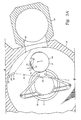
- Figures 3A-C are top views of the processing system 40 showing the blade 48 and substrate 37 in various positions during rotation through the transfer chamber 42.
- Figure 3A shows the blade 48 immediately after initiating counter-clockwise rotation so that the leading edge 92 of the substrate 37 is positioned in the path of the signal 54.
- a portion of the light pattern 53 represented by the shaded area, is shown intercepting the leading edge 92 of the substrate 37.
- the light pattern 53 scans the upper surface of the substrate 37.
- the light pattern 53 illuminates particles 75 on the substrate 37 which causes scattering of the signal 54.
- the size of the particles 75 are typically in the micron range but are shown greatly exaggerated for clarity.
- the scattered portion 74 of the signal 54 is then collected by the receiver unit 58. Where the detector 82 is a CCD, the scattered portion 64 is focused by the receiver optics 80, imaged onto the elements of the CCD, converted into an electrical signal and transmitted to the EPI 86 for processing.
- Figures 3A-C may represent a substrate being transferred from a load lock chamber to a processing chamber.
- Figures 3A-C may represent a processed chamber being transferred to a cooldown chamber or being returned to a load lock.
- Figures 2 and 3A-C show the preferred positioning and operation for the transmitter unit 56 and receiver unit 58
- the transmitter unit 56 and receiver unit 58 may be positioned at any point on the processing system 40 where the signal 54 may be directed onto the upper surface of a moving substrate and scattered light may be detected by the receiver unit 58.
- particle detection is performed during retraction or extension of the robot 50 as describe with reference to Figure 4.
- Figure 4 is a top of the processing system 40 showing the blade 48 and substrate 37 disposed thereon during the retraction of the blade 48 from the vacuum chamber 44 into the transfer chamber 42 via the aperture 46.
- the signal 54 preferably intercepts the substrate 37 in extreme proximity to the aperture 46 as shown in Figure 3A. Such a positioning ensures exposure of substantially the entire upper surface of the substrate after full retraction of the blade 48, thereby maximizing the surface area of the substrate 37 which is scanned by the signal 54.
- the shaded portion of the light pattern 53 indicates the portion of the signal 54 incident on the substrate 37.
- the substrate 37 is moved through the path of the signal 54, thereby exposing the upper surface of the substrate 37 to the signal 54.
- Particles 75 disposed on the upper surface of the substrate 37 cause the signal 54 to scatter, shown by arrows 74.
- the scattered portion of the signal 54 is collected by the receiver unit 58, converted into an electrical signal and transmitted to the EPI 86 for processing.
- the light pattern 53 is preferably radially outward of the trailing edge 98 of the substrate 37 so that the full surface area of the substrate 37 has been exposed to the light pattern 53.
- a pair of transmitter units 56 and receiver units 58 may be used in combination to monitor a substrate during linear motion and rotational motion, respectively. Such an arrangement can improve the accuracy of detection.
- a person skilled in the art will recognize other embodiments.
- additional methods may be employed to enhance detection confidence.
- the robot blade 48 may be dithered, or oscillated, so that a given particle can be moved into the field of view of another CCD detector element in the array of elements. Detection by multiple elements provides additional certainty of the existence and location of the particle.
- Determination of the location of a particle on the substrate is made by identifying particular features on the substrate or blade.
- the EPI may be programmed to detect the leading edge, i.e. , the substrate curvature which first enters the field-of-view of the receiver unit, and lagging edge, i.e. , the last curvature to be detected by the receiver unit, during linear or rotational movement of the substrate.
- the substrate edges provide reference points which may then be used to generate one of two coordinates, i.e., X and Y because the acquisition rate of the CCD detector is known.
- the acquisition rate refers to the frequency of image generation during the movement of the substrate in the field-of-view of the CCD detector.
- the processed output of the CCD detector is a "photograph" of the complete substrate surface.
- the remaining coordinate is determined by where the particle is detected on the detector array of the CCD detector.
- a cluster tool is a modular system comprising multiple chambers which perform various functions including substrate center-finding and orientation, degassing, annealing, deposition and/or etching.
- the multiple chambers are mounted to a central transfer chamber which houses a robot adapted to shuttle substrates between the chambers.
- the transfer chamber is typically maintained at a vacuum condition and provides an intermediate stage for shuttling substrates from one chamber to another and/or to a load lock chamber positioned at a front end of the cluster tool.
- the centralized position of the transfer chamber provides an ideal location for a particle detection system.
- FIG. 5 is a plan view of a typical cluster tool 100 for semiconductor processing wherein the present invention may be used to advantage.
- Two such platforms are the Centura® and the Endura® both available from Applied Materials, Inc., of Santa Clara, California.
- the details of one such staged-vacuum substrate processing system is disclosed in United States Patent No. 5,186,718, entitled “Staged-Vacuum Wafer Processing System and Method,” Tepman et al., issued on February 16, 1993, which is incorporated herein by reference.
- the exact arrangement and combination of chambers may be altered for purposes of performing specific steps of a fabrication process.
- the cluster tool 100 generally comprises a plurality of chambers and robots and is preferably equipped with a microprocessor controller 102 programmed to carry out the various processing methods performed in the cluster tool 100.
- a front-end environment 104 is shown positioned in selective communication with a pair of load lock chambers 106.
- a pod loader 108 disposed in the front-end environment 104 is capable of linear and rotational movement to shuttle cassettes of substrates between the load locks 106 and a plurality of pods 105 which are mounted on the front-end environment 104.
- the load locks 106 provide a first vacuum interface between the front-end environment 104 and a transfer chamber 110.
- Two load locks 106 are provided to increase throughput by alternatively communicating with the transfer chamber 110 and the front-end environment 104.
- a second load lock 106 communicates with the front-end environment 104.
- a robot 113 is centrally disposed in the transfer chamber 110 to transfer substrates from the load locks 106 to one of the various processing chambers 114 and service chambers 116.
- the processing chambers 114 may perform any number of processes such as physical vapor deposition, chemical vapor deposition, and etching while the service chambers 116 are adapted for degassing, orientation, cooldown and the like.
- a number of view ports 120 provide visual access into the transfer chamber 110.
- the view ports 120 provide suitable locations for the transmitter unit 56 and the receiver unit 58.
- Arrows 122, 124 indicate points where inspection of a substrate may be preformed.
- Arrows 122 represent points where the robot blade 126 is rotated and arrows 124 represent points where the robot blade 126 is extended or retracted.
- the transmitter unit 56 and receiver unit 58 may be positioned in the view ports 120 accordingly as described with reference to Figures 2-4.
- the transmitter unit 56 and receiver unit 58 may be secured above the view port 20 in a position having field of view of the robot blade 126 entering or exiting the load lock 106.
- the use of more than one transmitter unit 56 receiver unit 58 pair is also contemplated by the present invention.
- arrows 107 indicate the movement of substrates through other locations in the cluster tool 100 which provide additional inspection sites.
- the foregoing embodiments provide a detection apparatus and method capable of detecting the presence of particles on substrates on-the-fly and in situ. In situ, on-the-fly detection eliminates the need for conventional stand-alone inspection platforms comprising dedicated actuating mechanisms such as the stage 13 shown in Figure 1.
- the present invention uses to advantage components typically included in any conventional processing system, such as the robot 50 (shown in Figures 2-4), to enable a stageless inspection system. Particle detection is performed at various positions in a processing system during normal and necessary operation sequences without transferring the substrates to a separate stand-alone inspection platform, thereby minimizing the impact on throughput.
- each substrate entering or exiting the process system can be inspected, thereby achieving a significant improvement over prior art wherein only periodic sampling was possible due to the negative effect on overhead time.
- the use of conventional features such as view ports and transfer robots facilitates retrofitting the present invention to existing systems without the need for expensive re-machining procedures.
- the foregoing has been directed toward particle detection on unpatterned substrates having substantially smooth planar surfaces.
- light from the light source 60 shown in Figure 2
- Patterned substrates however include topological variances that can cause scattering of incident light, thereby falsely indicating the presence of a particle.
- the invention utilizes a unique signature produced by illuminating each substrate in order to differentiate between substrates.
- the unique signature is the result of the patterns formed on the substrate. Because the topology due to patterns of substrates that undergo a particular process is substantially repetitive, the signature will be unique for each of the substrates.
- the unique signature may be stored in a memory and used to compare surface conditions of substrates during production.
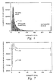
- Figure 6 represents a scan of 3 million data points showing the specular "signature" 150 for a calibration substrate scanned according to the techniques described above.
- the number of occurrences (y-axis), or readings by the detection equipment, at a particular intensity (x-axis) are plotted.
- two different test substrates were scanned in a similar manner resulting in two separate and distinct spectral signatures.
- the signatures for the two test substrates were compared to the signature 150 for the calibration substrate.
- the graphs 152, 154 shown in Figure 7 are the result of subtracting the number of occurrences at a given intensity for the calibration substrate from the number of occurrences at the same given intensity for the two test substrates.
- a first graph 152 represents the difference in the recorded output of the detection equipment between the first test substrate and the calibration substrate and shows little variation.
- a second graph 154 represents the difference in the recorded output of the detection equipment between the second test substrate and the calibration substrate and shows a significant variation, indicating a difference in the surface conditions of the compared substrates.
- the invention provides an efficient and effective method of comparing substrate surface conditions on-the-fly in a processing system.
- the invention is a viable method of determining whether production should be halted and a particular substrate should be examined more carefully for contamination or defects. Only selected substrates need undergo additional particle detection, thereby minimizing the impact to throughput.
- a preferred device In addition to particle detection, a preferred device would be capable of performing other functions typically performed in a processing chamber and inspection chamber in order to increase throughput and decrease operating cost.
- substrate characteristics such as discontinuity, (the presence of fractures and other structural defects) are important to identify potential problems which may affect the efficient operation of a system and lead to increased cost of operation due to damaged substrates.
- substrate centerfinding and orientation are often necessary steps during processing to generate positional information regarding substrates. In conventional systems such procedures are performed at designated locations in the processing system. Thus, a substrate must be shuttled to the designated locations in order to undergo each procedure, thereby decreasing throughput. Further, because such tests are typically performed only periodically on an arbitrary substrate, many substrates may be damaged before a problem is identified.
- a "gate-keeper" apparatus and method capable of examining a substrate for selected characteristics which include particles, orientation, centerfinding, reflectivity, substrate type, discontinuity, etc.
- a substrate for selected characteristics which include particles, orientation, centerfinding, reflectivity, substrate type, discontinuity, etc.
- an inspection can be performed prior to entry into a process chamber as well as exit from the process chamber, thereby determining real time pre- and post-processing conditions of the substrate.
- Robot behavior of interest includes acceleration, speed, repeatability, stability, etc.
- a system adapted to monitor such robot characteristics would provide an apparatus and method to ensure consistent robot behavior regardless of the particular system in which the robot is implemented.
- the inspection device described herein can be adapted to perform numerous other inventive uses needed in processing systems such as those just described, e.g., the determination of selected substrate characteristics including reflectivity, substrate type, discontinuity, orientation and centerfinding, as well as performing calibration of robots and the inspection equipment and monitoring robot behavior.
- substrate characteristics including reflectivity, substrate type, discontinuity, orientation and centerfinding
- the following discussion provides various embodiments for the present invention but is not intended to be exclusive, as those skilled in the art will readily recognize other possible embodiments.
- the invention determines the substrate type.
- the pattern of substrates provides a unique signature. Accordingly, the invention may be used to recognize substrates based on their pattern by scanning the substrate in the manner described above and transmitting the received signal to the EPI 86 for processing. The scanned pattern is then compared to stored signatures to determine the substrate type.
- Such an application provides the ability to detect a substrate that may have been misrouted through the system. For example, the OSA could detect and reject a substrate with photoresist which have been routed to a physical vapor deposition (PVD) chamber, thereby preventing potential damage to a process chamber and the substrate.
- recognition of the substrate pattern can be used to automatically change the process recipe according to the substrate type.
- the invention can be used to determine process uniformity, smoothness and substrate damage or defects, such as discontinuity (structural defects of the substrate due to thermal migration, for example, which may lead to portions of the substrate breaking off).
- the OSA and EPI 86 can be employed to generate a map of the substrate topology. The map can then be analyzed for texture characteristics such as planarity and uniformity.
- any substrate damage or defect, such as chips or fractures may be detected and mapped. Analysis can be enhanced by use of a color CCD detector.
- Another substrate characteristic which may be determined is the reflectivity of the substrate.
- Information regarding reflectivity can be used to determine whether certain process conditions have been successfully achieved, such as the endpoint of an etch process. Because the endpoint information is available in near real-time, i.e. , substantially contemporaneously with the end of the process, and proximate the processing chamber, an under-processed substrate may be immediately returned for additional processing. Conventionally, substrates are taken to a remote location for endpoint examination. A subsequent determination that a substrate is under-processed typically results in the substrate being discarded because the time involved in returning the substrate for additional processing is cost prohibitive.
- the invention provides for Optical Character Recognition (OCR).
- OCR refers to the detection and processing of alphanumeric characters through video imaging. Substrates are often identified by characters which are typically inscribed on the substrate surface.
- the transmitter unit 56 and the receiver unit 58 of the present invention provide an apparatus capable of illuminating and detecting the characters and then directing a signal to the EPI 86 for processing.
- a substrate is scanned in the manner described above.
- the signal 54 will strike the characters on the substrate and be reflected according to the geometry of the characters.
- the reflection is unique to the particular arrangement and configuration of the characters.
- the resulting signal can be compared to stored data representing previously scanned characters.
- the invention is used to determine a substrate's orientation and center. Orientation and center-finding are necessary to ensure proper positioning of the substrate in a chamber for particular processes. For example, etching involves the use of a mask to cover certain portions of the substrate surface. In order to position the mask on the appropriate portions of the substrate the orientation of the substrate must first be determined.
- the patterned surface of a properly oriented substrate on the blade provides a unique signature (as described above with reference to Figure 6) which can be stored in a computer system such as the EPI 86.
- the present invention can be used to verify the signature. As a substrate is moved into the optical path 61 of receiver unit 58, the receiver unit 58 determines whether the signature is correct. If the signature is verified the conventional orientation task can be bypassed, thereby increasing throughput.
- Substrate center-finding currently employs the use of one or more sensors to determine the center of a substrate.
- Use of the present invention enables substrate center-finding capability, thereby eliminating the need for additional sensors.
- the components of the invention may be located outside of the vacuum environment of a processing system, thereby eliminating outgassing problems associated with conventional arrangements.
- a substrate is illuminated and scanned by the OSA (i.e. , the transmitter unit 56 and the receiver unit 58) during the retraction, extension, and/or rotation of the blade.
- the OSA i.e. , the transmitter unit 56 and the receiver unit 58
- the receiver unit 58 ceases to detect a signal.
- the time between initial detection of a signal 54 and ceasing detection is recorded. For a known robot speed, the recorded time may be used to calculate the diameter of the substrate. If the substrate is determined not to be centered relative to a calibrated value, an adjustment is made to the destination coordinate of the robot 50 to correct the offset. It is understood that the particular method of calculating the substrate center is not limiting of the invention and people skilled in the art will recognize other possibilities.
- detection of the leading and lagging edges of a substrate may be associated with the encoder value of the robot 50 at the time of detection.
- the encoder values can then be compared to calibrated values for substrates of the same diameter to determine any offset that must be accommodated.
- a substrate's orientation and center can be found while the substrate is positioned in a chamber, such as a cool down chamber, a degas chamber, or any other chamber of a processing system such as the one shown in Figure 5.
- Center finding and orientation can be simultaneously done by positioning the substrate in the field of view of the receiver unit 58.
- the receiver unit 58 may be mounted in a view port of the chamber or in any other position wherein the receiver unit 58 can capture a substantial portion of the substrate in its field of view.
- the chamber acts both as an area for analysis of the substrate as well as performing a processing function such as cooling or degassing. As a result, analysis can proceed without affecting the throughput of the processing system.
- the transmitter unit 56 is adapted to provide annular illumination about the perimeter of the substrate.
- the transmitter unit 56 may be a light-ring taking the form of a fiber optic-based light-ring, such as those commercially available from Fostee of Auburn, New York, and especially configured for machine vision and microscopy application.
- the transmitter unit 56 is disposed at an upper end of the chamber opposite the substrate being examined.
- the side of the substrate facing the receiver unit 58 may be illuminated by the transmitter unit 56.
- the substrate is positioned against a uniform background in the chamber.
- the transmitter unit 56 then illuminates the surface of the substrate and the uniform background.
- the illumination provides an image which is captured by the receiver unit 58.
- the image is then transmitted to the EPI 86 for processing.
- Analysis of the image by the EPI 86 is accomplished by identifying a contrast in optical density. A change in contrast can be identified by comparing the optical density of one area of the image to optical density of another area of the image.
- analysis of the image taken by the receiver unit 58 will indicate a marked density contrast between the substrate and the uniform background.
- the dimension and shape of the substrate can be determined.
- analysis of the entire image provided by the receiver unit 58 will map the substrate perimeter indicating the position of an orientation notch. In this manner, the center and the orientation of the substrate can be found simultaneously.
- Optical density contrast refers to the change in contrast of the image received by the ESI 86 due to illumination of varying surfaces. Different surfaces (in the case the substrate and the background surface) produce different spectral results when illuminated, as described above with regard to spectral signatures. Such spectral variations can be analyzed by the EPI 86 to determine the dimensions of the substrate being illuminated.
- the transmitter unit 56 may be placed to illuminate the back side of the substrate. Accordingly, the transmitter unit 56 is sized to have an inner diameter slightly less than the diameter of the substrate and the outer diameter slightly greater than the diameter of the substrate. As a result, the illuminating radiation of the transmitter unit 56 is provided to a perimeter portion of the back side of the wafer. While the substrate blocks a portion of the illuminating radiation from the receiver unit 58, a portion of the radiation outside the diameter of the substrate is visible to the receiver unit 58, thereby enhancing optical density contrast at the substrate edge. The resulting image provides a relatively darker area corresponding to the area occupied by the substrate.
- the receiver unit 58 is preferably a two-dimensional CCD pixel array camera having lateral and vertical fields of view that span multiple pixels. In this manner, the acquired images provide multiple pixel rows and columns for quantification of a substrate's dimensions.
- a contrast analysis can be implemented using well known machine vision techniques and commercially available systems for executing the same.
- machine vision systems capable of implementing contrast analysis techniques are available from Cognex Corporation of Matick, Massachusetts.
- An example of a suitable machine vision system is the Cognex MVS 8000 series system, which includes a set of PC-based machine vision hardware and software tools. With such a system, the images can be analyzed on a pixel by pixel basis to evaluate optical density differences.
- the invention provides an apparatus and method for generating real-time information about selected characteristics of a substrate.
- Substrate inspection is preferably performed before and after processing.
- a preferred operation of the invention may be understood with reference to Figure 5.
- the invention Upon transfer of a substrate from the transfer chamber 110 into a process chamber 114 or service chamber 116 by the robot 113, the invention preferably operates to scan the substrate in the manner described above. The result of the scan then produces information regarding substrate type, orientation, centerfinding, discontinuity, specular signature and presence of particles. Following processing, these same characteristics may be determined during the retraction of the substrate from the processing or service chamber. Additionally, a determination may be made regarding the process results. For example, the reflected signal from the substrate scan may be used to generate information on process uniformity and the process endpoint in the manner described above.
- the invention provides real or near real-time pre- and post-processing information regarding characteristics of a substrate. Because the information is real-time an immediate cost efficient decision can be made about how to handle the substrate. Further, because each substrate may be inspected, as opposed to selected substrates from a batch, the information can be used to rectify identified problems with minimal damage to substrates and the processing environment.
- the invention is also adapted for calibration and health monitoring.
- the invention may be used to calibrate the detection devices. Because the illumination and detection optics of the invention will not be uniform, the operation must be normalized. Normalization will be accomplished in the following way.
- OSA the transmitter unit 56 and the receiver unit 58
- a substrate will be placed upside down on a robot blade. The robot blade will then move the substrate under the receiver unit 58.
- RMS root-mean-square
- the substrate is removed and the solid portion of the robot blade (i.e. , excluding holes and edges) is then scanned in a similar fashion.
- the peak-to-peak and average for each detector element is then compared to the normalized correction factors to determine the blade correction factors.
- the blade can act as a resident calibration reference.
- the OSA can monitor the empty blade during normal operation to determine if the optics 62, 80 are functioning properly. If the optics 62, 80 are contaminated, or a detector element of the detector 82 degrades, it will be detected by the foregoing background test.
- contamination disposed on the surface of the blade 48 is also detected by the test described in the foregoing embodiment. Contamination on the blade 48 indicates that the backsides of substrates are being scratched at some point during the handling of the substrate. Thus, if contamination is detected on the blade, the system can be halted for inspection, thereby preventing further contamination to the processing environment.
- the OSA facilitates robot calibration.
- the processing system robots such as the transfer chamber robot 50, periodically require calibration in order to ensure proper orientation and alignment.
- the OSA is mounted at a fixed location on a processing system, the OSA can provide a point of reference for the transfer chamber robot calibration.
- the blade features can be detected to verify the robot position and proportional, integral and differential (PID) values.
- PID proportional, integral and differential
- Sufficient variance between the detected position values and the calibrated position values stored by the EPI 86 indicates misalignment of the blade. The misalignment can be corrected by "homing" the robot according to the stored values.
- the invention also enables monitoring of robot behavior.
- the blade edge nearest to the center of rotation will enter into the optical path 61 first.
- This edge will then enter the field-of-views (FOVs) of each detector element successively at a rate which is determined by the blade velocity.
- FOVs field-of-views
- the collected data can be used to manually or automatically set the PID parameters of the robot.
- the invention may be used to detect the presence of a substrate on a robot blade as well as determining whether the substrate is in a blade clamp used to secure the substrate during the movement of the blade.
- a blade clamp used to secure the substrate during the movement of the blade.
- the invention facilitates the integration of numerous functions currently achieved by different components in a typical cluster tool.
- the program product is software readable by the EPI and includes code to generate at least substrate positional information, substrate reflectivity information, specular information, substrate defect information, substrate damage information, particle contamination information for smooth and patterned substrates, particle contamination information for the robot blade, alphanumeric character information, robot behavior information, calibration information for the robot and the detection devices and any combination thereof. It is understood that the foregoing list is merely illustrative and other functions may be performed by the invention.
Landscapes
- Physics & Mathematics (AREA)
- Health & Medical Sciences (AREA)
- Life Sciences & Earth Sciences (AREA)
- Chemical & Material Sciences (AREA)
- Analytical Chemistry (AREA)
- Biochemistry (AREA)
- General Health & Medical Sciences (AREA)
- General Physics & Mathematics (AREA)
- Immunology (AREA)
- Pathology (AREA)
- Investigating Materials By The Use Of Optical Means Adapted For Particular Applications (AREA)
- Testing Or Measuring Of Semiconductors Or The Like (AREA)
Applications Claiming Priority (2)
| Application Number | Priority Date | Filing Date | Title |
|---|---|---|---|
| US09/391,341 US6707544B1 (en) | 1999-09-07 | 1999-09-07 | Particle detection and embedded vision system to enhance substrate yield and throughput |
| US391341 | 1999-09-07 |
Publications (2)
| Publication Number | Publication Date |
|---|---|
| EP1083424A2 true EP1083424A2 (de) | 2001-03-14 |
| EP1083424A3 EP1083424A3 (de) | 2001-04-18 |
Family
ID=23546218
Family Applications (1)
| Application Number | Title | Priority Date | Filing Date |
|---|---|---|---|
| EP00307704A Withdrawn EP1083424A3 (de) | 1999-09-07 | 2000-09-07 | Partikel-Erkennung und optisches System um die Substrat-Produktion zu erhöhen |
Country Status (4)
| Country | Link |
|---|---|
| US (2) | US6707544B1 (de) |
| EP (1) | EP1083424A3 (de) |
| JP (1) | JP2001144153A (de) |
| KR (1) | KR100727168B1 (de) |
Cited By (29)
| Publication number | Priority date | Publication date | Assignee | Title |
|---|---|---|---|---|
| WO2002035217A3 (en) * | 2000-10-06 | 2002-08-15 | Applied Materials Inc | Methods for continuous embedded process monitoring and optical inspection of substrates using specular signature analysis |
| WO2002029390A3 (en) * | 2000-10-06 | 2003-04-17 | Applied Materials Inc | Method and apparatus to provide for automated process verification and hierarchical substrate examination |
| US6630995B1 (en) | 1999-09-07 | 2003-10-07 | Applied Materials, Inc. | Method and apparatus for embedded substrate and system status monitoring |
| WO2003075342A3 (en) * | 2002-03-01 | 2004-01-29 | Applied Materials Inc | Methodology for repeatable post etch cd in a production tool |
| WO2004001841A3 (en) * | 2002-06-20 | 2004-02-12 | Applied Materials Inc | Method and system for realtime critical dimention microloading control |
| US6693708B1 (en) | 1999-09-07 | 2004-02-17 | Applied Materials, Inc. | Method and apparatus for substrate surface inspection using spectral profiling techniques |
| US6697517B1 (en) | 1999-09-07 | 2004-02-24 | Applied Magerials, Inc. | Particle detection and embedded vision system to enhance substrate yield and throughput |
| US6707545B1 (en) | 1999-09-07 | 2004-03-16 | Applied Materials, Inc. | Optical signal routing method and apparatus providing multiple inspection collection points on semiconductor manufacturing systems |
| US6721045B1 (en) | 1999-09-07 | 2004-04-13 | Applied Materials, Inc. | Method and apparatus to provide embedded substrate process monitoring through consolidation of multiple process inspection techniques |
| US6813032B1 (en) | 1999-09-07 | 2004-11-02 | Applied Materials, Inc. | Method and apparatus for enhanced embedded substrate inspection through process data collection and substrate imaging techniques |
| US6909102B1 (en) | 2004-01-21 | 2005-06-21 | Varian Semiconductor Equipment Associates, Inc. | Ion implanter system, method and program product including particle detection |
| US6911399B2 (en) | 2003-09-19 | 2005-06-28 | Applied Materials, Inc. | Method of controlling critical dimension microloading of photoresist trimming process by selective sidewall polymer deposition |
| WO2005091342A3 (en) * | 2004-03-18 | 2005-11-17 | Axcelis Tech Inc | In-situ monitoring on a spinning-disk ion implanter |
| US7012684B1 (en) | 1999-09-07 | 2006-03-14 | Applied Materials, Inc. | Method and apparatus to provide for automated process verification and hierarchical substrate examination |
| US7265382B2 (en) | 2002-11-12 | 2007-09-04 | Applied Materials, Inc. | Method and apparatus employing integrated metrology for improved dielectric etch efficiency |
| US7498106B2 (en) | 2002-03-01 | 2009-03-03 | Applied Materials, Inc. | Method and apparatus for controlling etch processes during fabrication of semiconductor devices |
| US7601272B2 (en) | 2005-01-08 | 2009-10-13 | Applied Materials, Inc. | Method and apparatus for integrating metrology with etch processing |
| EP1419363A4 (de) * | 2001-07-02 | 2010-09-08 | Tevet Process Control Technolo | Verfahren und vorrichtung zum produktionslinien-screening |
| US7846848B2 (en) | 2005-01-08 | 2010-12-07 | Applied Materials, Inc. | Cluster tool with integrated metrology chamber for transparent substrates |
| CN103018261A (zh) * | 2012-11-29 | 2013-04-03 | 华中科技大学 | 一种rfid天线的外观缺陷检测系统及其方法 |
| EP1642113B1 (de) * | 2003-07-09 | 2014-04-09 | P.M.L. - Particles Monitoring Technologies Ltd. | Verfahren zur messung der partikelgrösse und -konzentration |
| CN103792197A (zh) * | 2014-01-28 | 2014-05-14 | 北京京东方显示技术有限公司 | 一种检测装置及检测方法 |
| CN109975802A (zh) * | 2019-04-04 | 2019-07-05 | 浙江大学 | 基于毫米波的反射变换成像系统及缺陷检测方法 |
| US10921229B2 (en) | 2011-12-01 | 2021-02-16 | Particle Measuring Systems, Inc. | Detection scheme for particle size and concentration measurement |
| US20210291374A1 (en) * | 2020-03-17 | 2021-09-23 | Applied Materials, Inc. | Calibration of an electronics processing system |
| US11237095B2 (en) | 2019-04-25 | 2022-02-01 | Particle Measuring Systems, Inc. | Particle detection systems and methods for on-axis particle detection and/or differential detection |
| US11781965B2 (en) | 2017-10-26 | 2023-10-10 | Particle Measuring Systems, Inc. | System and method for particles measurement |
| US11823937B2 (en) | 2019-08-19 | 2023-11-21 | Applied Materials, Inc. | Calibration of an aligner station of a processing system |
| US11988593B2 (en) | 2019-11-22 | 2024-05-21 | Particle Measuring Systems, Inc. | Advanced systems and methods for interferometric particle detection and detection of particles having small size dimensions |
Families Citing this family (55)
| Publication number | Priority date | Publication date | Assignee | Title |
|---|---|---|---|---|
| TW525213B (en) * | 2000-02-16 | 2003-03-21 | Hitachi Ltd | Process monitoring methods in a plasma processing apparatus, monitoring units, and a sample processing method using the monitoring units |
| JP2001291054A (ja) * | 2000-04-07 | 2001-10-19 | Nec Corp | 半導体ウエハのid認識装置及びid認識ソータシステム |
| JP2001304842A (ja) * | 2000-04-25 | 2001-10-31 | Hitachi Ltd | パターン検査方法及びその装置並びに基板の処理方法 |
| US6891627B1 (en) | 2000-09-20 | 2005-05-10 | Kla-Tencor Technologies Corp. | Methods and systems for determining a critical dimension and overlay of a specimen |
| US6673637B2 (en) | 2000-09-20 | 2004-01-06 | Kla-Tencor Technologies | Methods and systems for determining a presence of macro defects and overlay of a specimen |
| US7130029B2 (en) | 2000-09-20 | 2006-10-31 | Kla-Tencor Technologies Corp. | Methods and systems for determining an adhesion characteristic and a thickness of a specimen |
| US6694284B1 (en) | 2000-09-20 | 2004-02-17 | Kla-Tencor Technologies Corp. | Methods and systems for determining at least four properties of a specimen |
| US6812045B1 (en) | 2000-09-20 | 2004-11-02 | Kla-Tencor, Inc. | Methods and systems for determining a characteristic of a specimen prior to, during, or subsequent to ion implantation |
| US7349090B2 (en) | 2000-09-20 | 2008-03-25 | Kla-Tencor Technologies Corp. | Methods and systems for determining a property of a specimen prior to, during, or subsequent to lithography |
| US6782337B2 (en) | 2000-09-20 | 2004-08-24 | Kla-Tencor Technologies Corp. | Methods and systems for determining a critical dimension an a presence of defects on a specimen |
| US7106425B1 (en) | 2000-09-20 | 2006-09-12 | Kla-Tencor Technologies Corp. | Methods and systems for determining a presence of defects and a thin film characteristic of a specimen |
| US6919957B2 (en) | 2000-09-20 | 2005-07-19 | Kla-Tencor Technologies Corp. | Methods and systems for determining a critical dimension, a presence of defects, and a thin film characteristic of a specimen |
| WO2002025708A2 (en) | 2000-09-20 | 2002-03-28 | Kla-Tencor-Inc. | Methods and systems for semiconductor fabrication processes |
| DE10103253A1 (de) * | 2001-01-25 | 2002-08-01 | Leica Microsystems | Verfahren und Anordnung zum Transportieren und Inspizieren von Halbleitersubstraten |
| US20020196336A1 (en) * | 2001-06-19 | 2002-12-26 | Applied Materials, Inc. | Method and apparatus for substrate imaging |
| KR100452317B1 (ko) * | 2001-07-11 | 2004-10-12 | 삼성전자주식회사 | 포토리소그래피 공정시스템 및 그 방법 |
| US7024031B1 (en) * | 2001-10-23 | 2006-04-04 | August Technology Corp. | System and method for inspection using off-angle lighting |
| US7225047B2 (en) | 2002-03-19 | 2007-05-29 | Applied Materials, Inc. | Method, system and medium for controlling semiconductor wafer processes using critical dimension measurements |
| US7233841B2 (en) * | 2002-04-19 | 2007-06-19 | Applied Materials, Inc. | Vision system |
| US7085622B2 (en) * | 2002-04-19 | 2006-08-01 | Applied Material, Inc. | Vision system |
| JP4008291B2 (ja) * | 2002-06-10 | 2007-11-14 | 大日本スクリーン製造株式会社 | パターン検査装置、パターン検査方法およびプログラム |
| KR20040040737A (ko) * | 2002-11-07 | 2004-05-13 | 삼성전자주식회사 | 반도체 웨이퍼 검사 방법 및 장치 |
| US7525659B2 (en) * | 2003-01-15 | 2009-04-28 | Negevtech Ltd. | System for detection of water defects |
| US6919101B2 (en) * | 2003-02-04 | 2005-07-19 | Tegal Corporation | Method to deposit an impermeable film on porous low-k dielectric film |
| US7177487B2 (en) * | 2003-04-21 | 2007-02-13 | Baxter International Inc. | Determination of particle size by image analysis |
| US10086511B2 (en) | 2003-11-10 | 2018-10-02 | Brooks Automation, Inc. | Semiconductor manufacturing systems |
| US8812150B2 (en) * | 2003-11-10 | 2014-08-19 | Brooks Automation, Inc. | Semiconductor manufacturing process modules |
| US8313277B2 (en) * | 2003-11-10 | 2012-11-20 | Brooks Automation, Inc. | Semiconductor manufacturing process modules |
| US8696298B2 (en) * | 2003-11-10 | 2014-04-15 | Brooks Automation, Inc. | Semiconductor manufacturing process modules |
| KR101027562B1 (ko) * | 2003-12-31 | 2011-04-06 | 동부일렉트로닉스 주식회사 | 쿨다운챔버의 파손웨이퍼검출장치 및 검출방법 |
| KR100598381B1 (ko) | 2004-06-18 | 2006-07-07 | 삼성전자주식회사 | 인-라인 타입의 자동 웨이퍼결함 분류장치 및 그 제어방법 |
| KR100717553B1 (ko) * | 2004-11-18 | 2007-05-15 | 가부시키가이샤 탑콘 | 입자 모니터링 장치 및 진공 처리 장치 |
| WO2006055984A2 (en) * | 2004-11-22 | 2006-05-26 | Applied Materials, Inc. | Substrate processing apparatus using a batch processing chamber |
| US20070196011A1 (en) * | 2004-11-22 | 2007-08-23 | Cox Damon K | Integrated vacuum metrology for cluster tool |
| US7396412B2 (en) * | 2004-12-22 | 2008-07-08 | Sokudo Co., Ltd. | Coat/develop module with shared dispense |
| US7798764B2 (en) | 2005-12-22 | 2010-09-21 | Applied Materials, Inc. | Substrate processing sequence in a cartesian robot cluster tool |
| DE602006013409D1 (de) * | 2005-01-17 | 2010-05-20 | Biophos Ag | Verfahren und vorrichtung zur messung dynamischer partikelparameter |
| PL1910823T3 (pl) | 2005-07-26 | 2016-04-29 | Bayer Healthcare Llc | Sposób i system do sprawdzania elektromechanicznego biosensora |
| WO2007061383A1 (en) * | 2005-11-25 | 2007-05-31 | Agency For Science, Technology & Research | Determination of field distribution |
| KR100738809B1 (ko) * | 2006-02-01 | 2007-07-12 | 동부일렉트로닉스 주식회사 | 웨이퍼 표면 검사 시스템 및 그 제어방법 |
| US8031931B2 (en) * | 2006-04-24 | 2011-10-04 | Applied Materials South East Asia Pte. Ltd. | Printed fourier filtering in optical inspection tools |
| JP2009544024A (ja) * | 2006-07-17 | 2009-12-10 | ビオフォス アクチエンゲゼルシャフト | 画像相関によるモバイル粒子分析装置 |
| JP5064835B2 (ja) * | 2007-02-28 | 2012-10-31 | 株式会社アルバック | 基板搬送装置 |
| DE102007036814A1 (de) * | 2007-08-03 | 2009-02-12 | Vistec Semiconductor Systems Gmbh | Koordinaten-Messmaschine zum Vermessen von Strukturen auf einem Substrat |
| US8260461B2 (en) * | 2007-08-30 | 2012-09-04 | Applied Materials, Inc. | Method and system for robot calibrations with a camera |
| US8224607B2 (en) | 2007-08-30 | 2012-07-17 | Applied Materials, Inc. | Method and apparatus for robot calibrations with a calibrating device |
| KR101037724B1 (ko) * | 2009-03-04 | 2011-05-30 | (주)한국시스톰 | 웨이퍼 손상 방지 시스템 및 방법 |
| CN102378909B (zh) | 2009-04-30 | 2014-07-02 | 威尔科克斯联营公司 | 检查方法和检查装置 |
| TWI408766B (zh) * | 2009-11-12 | 2013-09-11 | 日立全球先端科技股份有限公司 | Vacuum processing device |
| US10648927B2 (en) * | 2015-05-15 | 2020-05-12 | Taiwan Semiconductor Manufacturing Company Ltd. | Method and apparatus for monitoring edge bevel removal area in semiconductor apparatus and electroplating system |
| WO2017205391A1 (en) * | 2016-05-23 | 2017-11-30 | Applied Materials, Inc. | Particle detection for substrate processing |
| US9725302B1 (en) * | 2016-08-25 | 2017-08-08 | Applied Materials, Inc. | Wafer processing equipment having exposable sensing layers |
| KR102374612B1 (ko) * | 2019-08-22 | 2022-03-15 | 삼성디스플레이 주식회사 | 레이저 장치 및 레이저 가공 방법 |
| KR20220162896A (ko) * | 2021-06-01 | 2022-12-09 | 삼성디스플레이 주식회사 | 레이저 가공 장치 및 레이저 가공 방법 |
| EP4359775A4 (de) * | 2021-06-24 | 2025-05-14 | LAM Research Corporation | Inline-maschinensichtsystem zur teileverfolgung eines substratverarbeitungssystems |
Family Cites Families (77)
| Publication number | Priority date | Publication date | Assignee | Title |
|---|---|---|---|---|
| JPS57132044A (en) | 1981-02-10 | 1982-08-16 | Hitachi Metals Ltd | Discriminating method of surface defect |
| US4499595A (en) | 1981-10-01 | 1985-02-12 | General Electric Co. | System and method for pattern recognition |
| US4441124A (en) | 1981-11-05 | 1984-04-03 | Western Electric Company, Inc. | Technique for inspecting semiconductor wafers for particulate contamination |
| EP0119198A4 (de) * | 1982-09-20 | 1986-07-08 | Contrex Inc | Selbsttätiges halbleiter-oberflächenkontrollgerät und verfahren. |
| EP0146005B1 (de) | 1983-11-26 | 1991-08-28 | Kabushiki Kaisha Toshiba | Apparat zum Nachweis von Oberflächenfehlern |
| US4920385A (en) | 1984-02-14 | 1990-04-24 | Diffracto Ltd. | Panel surface flaw inspection |
| IL79097A0 (en) | 1985-06-17 | 1986-09-30 | Visionetics Corp | Automatic optical inspection of printed circuit boards |
| US4893932A (en) | 1986-05-02 | 1990-01-16 | Particle Measuring Systems, Inc. | Surface analysis system and method |
| US4772126A (en) | 1986-10-23 | 1988-09-20 | Inspex Incorporated | Particle detection method and apparatus |
| US4880348A (en) * | 1987-05-15 | 1989-11-14 | Roboptek, Inc. | Wafer centration device |
| US4898471A (en) | 1987-06-18 | 1990-02-06 | Tencor Instruments | Particle detection on patterned wafers and the like |
| US4989973A (en) | 1988-10-03 | 1991-02-05 | Nissan Motor Co., Ltd. | Surface condition estimating apparatus |
| US4977330A (en) | 1989-02-13 | 1990-12-11 | Batchelder Tom W | In-line photoresist thickness monitor |
| US4941980A (en) | 1989-02-17 | 1990-07-17 | Opal, Inc. | System for measuring a topographical feature on a specimen |
| US4969748A (en) | 1989-04-13 | 1990-11-13 | Peak Systems, Inc. | Apparatus and method for compensating for errors in temperature measurement of semiconductor wafers during rapid thermal processing |
| US5127726A (en) | 1989-05-19 | 1992-07-07 | Eastman Kodak Company | Method and apparatus for low angle, high resolution surface inspection |
| US5186718A (en) | 1989-05-19 | 1993-02-16 | Applied Materials, Inc. | Staged-vacuum wafer processing system and method |
| NL8902471A (nl) | 1989-10-05 | 1991-05-01 | Philips Nv | Tweetraps positioneerinrichting. |
| US5058178A (en) | 1989-12-21 | 1991-10-15 | At&T Bell Laboratories | Method and apparatus for inspection of specular, three-dimensional features |
| JP2843424B2 (ja) * | 1990-06-26 | 1999-01-06 | 株式会社日立製作所 | 半導体製造工程の量産立上げ及び量産ラインの異物検査方法及びその装置 |
| US5233191A (en) | 1990-04-02 | 1993-08-03 | Hitachi, Ltd. | Method and apparatus of inspecting foreign matters during mass production start-up and mass production line in semiconductor production process |
| US5274434A (en) | 1990-04-02 | 1993-12-28 | Hitachi, Ltd. | Method and apparatus for inspecting foreign particles on real time basis in semiconductor mass production line |
| JPH04152545A (ja) * | 1990-10-17 | 1992-05-26 | Hitachi Ltd | 異物検査方法 |
| JPH04179141A (ja) * | 1990-11-09 | 1992-06-25 | Nec Yamagata Ltd | ウェーハにおける文字読取り装置 |
| IL99823A0 (en) | 1990-11-16 | 1992-08-18 | Orbot Instr Ltd | Optical inspection method and apparatus |
| JPH08250385A (ja) * | 1995-03-14 | 1996-09-27 | Hitachi Ltd | 半導体生産方法及びそのシステム |
| US5463459A (en) | 1991-04-02 | 1995-10-31 | Hitachi, Ltd. | Method and apparatus for analyzing the state of generation of foreign particles in semiconductor fabrication process |
| US5317656A (en) | 1991-05-17 | 1994-05-31 | Texas Instruments Incorporated | Fiber optic network for multi-point emissivity-compensated semiconductor wafer pyrometry |
| US5177559A (en) | 1991-05-17 | 1993-01-05 | International Business Machines Corporation | Dark field imaging defect inspection system for repetitive pattern integrated circuits |
| US5563702A (en) | 1991-08-22 | 1996-10-08 | Kla Instruments Corporation | Automated photomask inspection apparatus and method |
| US5486919A (en) | 1992-04-27 | 1996-01-23 | Canon Kabushiki Kaisha | Inspection method and apparatus for inspecting a particle, if any, on a substrate having a pattern |
| US5737122A (en) | 1992-05-01 | 1998-04-07 | Electro Scientific Industries, Inc. | Illumination system for OCR of indicia on a substrate |
| JPH05322781A (ja) * | 1992-05-19 | 1993-12-07 | Sony Corp | 表面異物検査装置 |
| EP0597637B1 (de) | 1992-11-12 | 2000-08-23 | Applied Materials, Inc. | System und Verfahren für automatische Positionierung eines Substrats in einem Prozessraum |
| US5861952A (en) | 1992-11-16 | 1999-01-19 | Canon Kabushiki Kaisha | Optical inspection method and apparatus including intensity modulation of a light beam and detection of light scattered at an inspection position |
| US5637881A (en) | 1993-04-01 | 1997-06-10 | High Yield Technology, Inc. | Method to detect non-spherical particles using orthogonally polarized light |
| US5808735A (en) | 1993-06-17 | 1998-09-15 | Ultrapointe Corporation | Method for characterizing defects on semiconductor wafers |
| US5479252A (en) | 1993-06-17 | 1995-12-26 | Ultrapointe Corporation | Laser imaging system for inspection and analysis of sub-micron particles |
| US5416594A (en) | 1993-07-20 | 1995-05-16 | Tencor Instruments | Surface scanner with thin film gauge |
| DE69322775T2 (de) | 1993-08-12 | 1999-07-22 | International Business Machines Corp., Armonk, N.Y. | Verfahren zur Inspektion vom Verbindungskugel-Satz eines intergrierten Schaltungsmoduls |
| US5663569A (en) | 1993-10-14 | 1997-09-02 | Nikon Corporation | Defect inspection method and apparatus, and defect display method |
| US5578832A (en) | 1994-09-02 | 1996-11-26 | Affymetrix, Inc. | Method and apparatus for imaging a sample on a device |
| US5563798A (en) | 1994-04-05 | 1996-10-08 | Applied Materials, Inc. | Wafer positioning system |
| US5465152A (en) | 1994-06-03 | 1995-11-07 | Robotic Vision Systems, Inc. | Method for coplanarity inspection of package or substrate warpage for ball grid arrays, column arrays, and similar structures |
| US5864394A (en) | 1994-06-20 | 1999-01-26 | Kla-Tencor Corporation | Surface inspection system |
| US5883710A (en) | 1994-12-08 | 1999-03-16 | Kla-Tencor Corporation | Scanning system for inspecting anomalies on surfaces |
| US5774222A (en) | 1994-10-07 | 1998-06-30 | Hitachi, Ltd. | Manufacturing method of semiconductor substrative and method and apparatus for inspecting defects of patterns on an object to be inspected |
| EP0718624A3 (de) | 1994-12-19 | 1997-07-30 | At & T Corp | Vorrichtung und Verfahren zur Beleuchtung durchsichtiger und halbtransparenter Materialien |
| JPH08178857A (ja) | 1994-12-21 | 1996-07-12 | Nikon Corp | 大型基板用異物検査装置 |
| US5805278A (en) | 1995-02-09 | 1998-09-08 | Inspex, Inc. | Particle detection method and apparatus |
| JPH08264606A (ja) * | 1995-03-27 | 1996-10-11 | Hitachi Ltd | 真空中処理基板検査装置 |
| US5903342A (en) | 1995-04-10 | 1999-05-11 | Hitachi Electronics Engineering, Co., Ltd. | Inspection method and device of wafer surface |
| US5659172A (en) | 1995-06-21 | 1997-08-19 | Opal Technologies Ltd. | Reliable defect detection using multiple perspective scanning electron microscope images |
| JP3140664B2 (ja) | 1995-06-30 | 2001-03-05 | 松下電器産業株式会社 | 異物検査方法及び装置 |
| US5644393A (en) | 1995-10-19 | 1997-07-01 | Hitachi Electronics Engineering Co., Ltd. | Extraneous substance inspection method and apparatus |
| KR970030586A (ko) * | 1995-11-14 | 1997-06-26 | 오노 시게오 | 웨이퍼 검사장치 |
| US5818576A (en) | 1995-11-28 | 1998-10-06 | Hitachi Electronics Engineering Co., Ltd. | Extraneous substance inspection apparatus for patterned wafer |
| US5694214A (en) | 1996-01-08 | 1997-12-02 | Hitachi Electronics Engineering Co., Ltd. | Surface inspection method and apparatus |
| JPH09196859A (ja) | 1996-01-23 | 1997-07-31 | Nec Corp | 表面欠陥検査装置 |
| US5822213A (en) | 1996-03-29 | 1998-10-13 | Lam Research Corporation | Method and apparatus for determining the center and orientation of a wafer-like object |
| US6012966A (en) | 1996-05-10 | 2000-01-11 | Canon Kabushiki Kaisha | Precision polishing apparatus with detecting means |
| US5905850A (en) * | 1996-06-28 | 1999-05-18 | Lam Research Corporation | Method and apparatus for positioning substrates |
| US5912732A (en) | 1996-07-05 | 1999-06-15 | Kabushiki Kaisha Topcon | Surface detecting apparatus |
| US5781693A (en) | 1996-07-24 | 1998-07-14 | Applied Materials, Inc. | Gas introduction showerhead for an RTP chamber with upper and lower transparent plates and gas flow therebetween |
| IL119213A (en) | 1996-09-06 | 2000-08-31 | Orbot Instr Ltd | Universal chuck for holding plates of various sizes |
| KR19980027352A (ko) * | 1996-10-15 | 1998-07-15 | 김광호 | 웨이퍼 개별 데이터 관리 시스템 |
| US5940175A (en) | 1996-11-01 | 1999-08-17 | Msp Corporation | Method and apparatus for surface inspection in a chamber |
| US5801824A (en) | 1996-11-25 | 1998-09-01 | Photon Dynamics, Inc. | Large area defect monitor tool for manufacture of clean surfaces |
| US5889593A (en) | 1997-02-26 | 1999-03-30 | Kla Instruments Corporation | Optical system and method for angle-dependent reflection or transmission measurement |
| US5909276A (en) | 1997-03-31 | 1999-06-01 | Microtherm, Llc | Optical inspection module and method for detecting particles and defects on substrates in integrated process tools |
| AU8472898A (en) | 1997-06-30 | 1999-01-19 | Semiconductor Technologies & Instruments, Inc. | Method and apparatus for inspecting a workpiece |
| KR19990027324A (ko) | 1997-09-29 | 1999-04-15 | 윤종용 | 웨이퍼 인식 시스템을 구비하는 멀티 챔버 시스템과 이를 이용한 웨이퍼 가공방법 |
| US5900633A (en) | 1997-12-15 | 1999-05-04 | On-Line Technologies, Inc | Spectrometric method for analysis of film thickness and composition on a patterned sample |
| US6208751B1 (en) | 1998-03-24 | 2001-03-27 | Applied Materials, Inc. | Cluster tool |
| US6020957A (en) | 1998-04-30 | 2000-02-01 | Kla-Tencor Corporation | System and method for inspecting semiconductor wafers |
| US6327374B1 (en) | 1999-02-18 | 2001-12-04 | Thermo Radiometrie Oy | Arrangement and method for inspection of surface quality |
| US6707544B1 (en) | 1999-09-07 | 2004-03-16 | Applied Materials, Inc. | Particle detection and embedded vision system to enhance substrate yield and throughput |
-
1999
- 1999-09-07 US US09/391,341 patent/US6707544B1/en not_active Expired - Fee Related
-
2000
- 2000-04-10 US US09/546,644 patent/US6697517B1/en not_active Expired - Fee Related
- 2000-09-07 EP EP00307704A patent/EP1083424A3/de not_active Withdrawn
- 2000-09-07 KR KR1020000053137A patent/KR100727168B1/ko not_active Expired - Fee Related
- 2000-09-07 JP JP2000271829A patent/JP2001144153A/ja active Pending
Cited By (41)
| Publication number | Priority date | Publication date | Assignee | Title |
|---|---|---|---|---|
| US6813032B1 (en) | 1999-09-07 | 2004-11-02 | Applied Materials, Inc. | Method and apparatus for enhanced embedded substrate inspection through process data collection and substrate imaging techniques |
| US6630995B1 (en) | 1999-09-07 | 2003-10-07 | Applied Materials, Inc. | Method and apparatus for embedded substrate and system status monitoring |
| US7012684B1 (en) | 1999-09-07 | 2006-03-14 | Applied Materials, Inc. | Method and apparatus to provide for automated process verification and hierarchical substrate examination |
| US6693708B1 (en) | 1999-09-07 | 2004-02-17 | Applied Materials, Inc. | Method and apparatus for substrate surface inspection using spectral profiling techniques |
| US6697517B1 (en) | 1999-09-07 | 2004-02-24 | Applied Magerials, Inc. | Particle detection and embedded vision system to enhance substrate yield and throughput |
| US6707544B1 (en) | 1999-09-07 | 2004-03-16 | Applied Materials, Inc. | Particle detection and embedded vision system to enhance substrate yield and throughput |
| US6707545B1 (en) | 1999-09-07 | 2004-03-16 | Applied Materials, Inc. | Optical signal routing method and apparatus providing multiple inspection collection points on semiconductor manufacturing systems |
| US6721045B1 (en) | 1999-09-07 | 2004-04-13 | Applied Materials, Inc. | Method and apparatus to provide embedded substrate process monitoring through consolidation of multiple process inspection techniques |
| WO2002029390A3 (en) * | 2000-10-06 | 2003-04-17 | Applied Materials Inc | Method and apparatus to provide for automated process verification and hierarchical substrate examination |
| WO2002035217A3 (en) * | 2000-10-06 | 2002-08-15 | Applied Materials Inc | Methods for continuous embedded process monitoring and optical inspection of substrates using specular signature analysis |
| EP1419363A4 (de) * | 2001-07-02 | 2010-09-08 | Tevet Process Control Technolo | Verfahren und vorrichtung zum produktionslinien-screening |
| US6858361B2 (en) | 2002-03-01 | 2005-02-22 | David S. L. Mui | Methodology for repeatable post etch CD in a production tool |
| WO2003075342A3 (en) * | 2002-03-01 | 2004-01-29 | Applied Materials Inc | Methodology for repeatable post etch cd in a production tool |
| US7498106B2 (en) | 2002-03-01 | 2009-03-03 | Applied Materials, Inc. | Method and apparatus for controlling etch processes during fabrication of semiconductor devices |
| US6924088B2 (en) | 2002-06-20 | 2005-08-02 | Applied Materials, Inc. | Method and system for realtime CD microloading control |
| WO2004001841A3 (en) * | 2002-06-20 | 2004-02-12 | Applied Materials Inc | Method and system for realtime critical dimention microloading control |
| US7265382B2 (en) | 2002-11-12 | 2007-09-04 | Applied Materials, Inc. | Method and apparatus employing integrated metrology for improved dielectric etch efficiency |
| EP1642113B1 (de) * | 2003-07-09 | 2014-04-09 | P.M.L. - Particles Monitoring Technologies Ltd. | Verfahren zur messung der partikelgrösse und -konzentration |
| US6911399B2 (en) | 2003-09-19 | 2005-06-28 | Applied Materials, Inc. | Method of controlling critical dimension microloading of photoresist trimming process by selective sidewall polymer deposition |
| US6909102B1 (en) | 2004-01-21 | 2005-06-21 | Varian Semiconductor Equipment Associates, Inc. | Ion implanter system, method and program product including particle detection |
| WO2005091342A3 (en) * | 2004-03-18 | 2005-11-17 | Axcelis Tech Inc | In-situ monitoring on a spinning-disk ion implanter |
| US7601272B2 (en) | 2005-01-08 | 2009-10-13 | Applied Materials, Inc. | Method and apparatus for integrating metrology with etch processing |
| US7846848B2 (en) | 2005-01-08 | 2010-12-07 | Applied Materials, Inc. | Cluster tool with integrated metrology chamber for transparent substrates |
| US12313514B2 (en) | 2011-12-01 | 2025-05-27 | Particle Measuring Systems, Inc. | Detection scheme for particle size and concentration measurement |
| US10921229B2 (en) | 2011-12-01 | 2021-02-16 | Particle Measuring Systems, Inc. | Detection scheme for particle size and concentration measurement |
| CN103018261B (zh) * | 2012-11-29 | 2015-03-04 | 华中科技大学 | 一种rfid天线的外观缺陷检测系统及其方法 |
| CN103018261A (zh) * | 2012-11-29 | 2013-04-03 | 华中科技大学 | 一种rfid天线的外观缺陷检测系统及其方法 |
| CN103792197A (zh) * | 2014-01-28 | 2014-05-14 | 北京京东方显示技术有限公司 | 一种检测装置及检测方法 |
| US12399102B2 (en) | 2017-10-26 | 2025-08-26 | Particle Measuring Systems, Inc. | System and method for particles measurement |
| US11781965B2 (en) | 2017-10-26 | 2023-10-10 | Particle Measuring Systems, Inc. | System and method for particles measurement |
| CN109975802A (zh) * | 2019-04-04 | 2019-07-05 | 浙江大学 | 基于毫米波的反射变换成像系统及缺陷检测方法 |
| US11237095B2 (en) | 2019-04-25 | 2022-02-01 | Particle Measuring Systems, Inc. | Particle detection systems and methods for on-axis particle detection and/or differential detection |
| US11946852B2 (en) | 2019-04-25 | 2024-04-02 | Particle Measuring Systems, Inc. | Particle detection systems and methods for on-axis particle detection and/or differential detection |
| US12615997B2 (en) | 2019-08-19 | 2026-04-28 | Applied Materials, Inc. | Calibration of an aligner station of a processing system |
| US11823937B2 (en) | 2019-08-19 | 2023-11-21 | Applied Materials, Inc. | Calibration of an aligner station of a processing system |
| US11988593B2 (en) | 2019-11-22 | 2024-05-21 | Particle Measuring Systems, Inc. | Advanced systems and methods for interferometric particle detection and detection of particles having small size dimensions |
| WO2021188581A1 (en) * | 2020-03-17 | 2021-09-23 | Applied Materials, Inc. | Calibration of an electronics processing system |
| US12115683B2 (en) | 2020-03-17 | 2024-10-15 | Applied Materials, Inc. | Calibration of an electronics processing system |
| US11766782B2 (en) | 2020-03-17 | 2023-09-26 | Applied Materials, Inc. | Calibration of an electronics processing system |
| US11759954B2 (en) * | 2020-03-17 | 2023-09-19 | Applied Materials, Inc. | Calibration of an electronics processing system |
| US20210291374A1 (en) * | 2020-03-17 | 2021-09-23 | Applied Materials, Inc. | Calibration of an electronics processing system |
Also Published As
| Publication number | Publication date |
|---|---|
| JP2001144153A (ja) | 2001-05-25 |
| EP1083424A3 (de) | 2001-04-18 |
| KR20010030320A (ko) | 2001-04-16 |
| KR100727168B1 (ko) | 2007-06-13 |
| US6697517B1 (en) | 2004-02-24 |
| US6707544B1 (en) | 2004-03-16 |
Similar Documents
| Publication | Publication Date | Title |
|---|---|---|
| US6707544B1 (en) | Particle detection and embedded vision system to enhance substrate yield and throughput | |
| US6813032B1 (en) | Method and apparatus for enhanced embedded substrate inspection through process data collection and substrate imaging techniques | |
| US6721045B1 (en) | Method and apparatus to provide embedded substrate process monitoring through consolidation of multiple process inspection techniques | |
| US6630995B1 (en) | Method and apparatus for embedded substrate and system status monitoring | |
| US6707545B1 (en) | Optical signal routing method and apparatus providing multiple inspection collection points on semiconductor manufacturing systems | |
| US7012684B1 (en) | Method and apparatus to provide for automated process verification and hierarchical substrate examination | |
| US6693708B1 (en) | Method and apparatus for substrate surface inspection using spectral profiling techniques | |
| US6882416B1 (en) | Methods for continuous embedded process monitoring and optical inspection of substrates using specular signature analysis | |
| EP1016126B1 (de) | Optisches inspektionsmodul und verfahren zur detektion von teilchen und defekten auf substraten in integrierten prozesswerkzeugen | |
| US9529279B2 (en) | Method and apparatus for inspecting a substrate | |
| JP5097335B2 (ja) | プロセス変動のモニタシステムおよび方法 | |
| KR100871495B1 (ko) | 자동 프로세스 검증 및 계층적 기판 검사를 위한 방법 및장치 | |
| JP2000068361A (ja) | 半導体の製造装置及びウェ―ハのアライメント状態を決定する方法 | |
| JP2000315712A (ja) | 半導体デバイスの生産方法 | |
| JP4876744B2 (ja) | 検査装置 | |
| JPH11274256A (ja) | 試料検査装置 | |
| KR100255253B1 (ko) | 반도체의 생산방법 및 그 제조 설비 |
Legal Events
| Date | Code | Title | Description |
|---|---|---|---|
| PUAI | Public reference made under article 153(3) epc to a published international application that has entered the european phase |
Free format text: ORIGINAL CODE: 0009012 |
|
| PUAL | Search report despatched |
Free format text: ORIGINAL CODE: 0009013 |
|
| AK | Designated contracting states |
Kind code of ref document: A2 Designated state(s): AT BE CH CY DE DK ES FI FR GB GR IE IT LI LU MC NL PT SE |
|
| AX | Request for extension of the european patent |
Free format text: AL;LT;LV;MK;RO;SI |
|
| RIC1 | Information provided on ipc code assigned before grant |
Free format text: 7G 01N 21/94 A, 7G 01N 21/95 B, 7G 01N 21/88 B, 7G 01N 21/956 B |
|
| AK | Designated contracting states |
Kind code of ref document: A3 Designated state(s): AT BE CH CY DE DK ES FI FR GB GR IE IT LI LU MC NL PT SE |
|
| AX | Request for extension of the european patent |
Free format text: AL;LT;LV;MK;RO;SI |
|
| 17P | Request for examination filed |
Effective date: 20011001 |
|
| AKX | Designation fees paid |
Free format text: BE DE GB NL |
|
| 17Q | First examination report despatched |
Effective date: 20040219 |
|
| STAA | Information on the status of an ep patent application or granted ep patent |
Free format text: STATUS: THE APPLICATION IS DEEMED TO BE WITHDRAWN |
|
| 18D | Application deemed to be withdrawn |
Effective date: 20050517 |