EP1083436A1 - Procédé et circuit de test de la présence de multiples tensions d'alimentations dans un circuit integré - Google Patents
Procédé et circuit de test de la présence de multiples tensions d'alimentations dans un circuit integré Download PDFInfo
- Publication number
- EP1083436A1 EP1083436A1 EP99830559A EP99830559A EP1083436A1 EP 1083436 A1 EP1083436 A1 EP 1083436A1 EP 99830559 A EP99830559 A EP 99830559A EP 99830559 A EP99830559 A EP 99830559A EP 1083436 A1 EP1083436 A1 EP 1083436A1
- Authority
- EP
- European Patent Office
- Prior art keywords
- voltage
- signal
- ramp
- capacitor
- supply voltages
- Prior art date
- Legal status (The legal status is an assumption and is not a legal conclusion. Google has not performed a legal analysis and makes no representation as to the accuracy of the status listed.)
- Granted
Links
- 238000000034 method Methods 0.000 title claims abstract description 17
- 239000003990 capacitor Substances 0.000 claims abstract description 42
- 238000012544 monitoring process Methods 0.000 claims abstract description 8
- 230000003750 conditioning effect Effects 0.000 claims description 2
- 230000003247 decreasing effect Effects 0.000 claims 1
- 238000010586 diagram Methods 0.000 description 5
- 230000001105 regulatory effect Effects 0.000 description 3
- 230000007704 transition Effects 0.000 description 2
- 238000012795 verification Methods 0.000 description 2
- 238000001914 filtration Methods 0.000 description 1
- 230000000873 masking effect Effects 0.000 description 1
- 230000000630 rising effect Effects 0.000 description 1
- 230000001052 transient effect Effects 0.000 description 1
Images


Classifications
-
- G—PHYSICS
- G01—MEASURING; TESTING
- G01R—MEASURING ELECTRIC VARIABLES; MEASURING MAGNETIC VARIABLES
- G01R31/00—Arrangements for testing electric properties; Arrangements for locating electric faults; Arrangements for electrical testing characterised by what is being tested not provided for elsewhere
- G01R31/40—Testing power supplies
-
- G—PHYSICS
- G05—CONTROLLING; REGULATING
- G05F—SYSTEMS FOR REGULATING ELECTRIC OR MAGNETIC VARIABLES
- G05F1/00—Automatic systems in which deviations of an electric quantity from one or more predetermined values are detected at the output of the system and fed back to a device within the system to restore the detected quantity to its predetermined value or values, i.e. retroactive systems
- G05F1/10—Regulating voltage or current
- G05F1/46—Regulating voltage or current wherein the variable actually regulated by the final control device is DC
- G05F1/468—Regulating voltage or current wherein the variable actually regulated by the final control device is DC characterised by reference voltage circuitry, e.g. soft start, remote shutdown
Definitions
- the invention relates to integrated digital circuits and in particular to the procedures for monitoring the correct presence of all supplies, a function referred to as "power monitor”.
- supply voltage sources are externally provided, others are implemented internally by as many voltage regulators that are referred to one or the other of the externally generated supply voltages.
- this signal is acknowledged at the end of the charging process of a capacitor charged with a relatively low constant current such to prevent the functional circuits to produce false switchings because of an insufficient supply voltage at the turn-on of the IC.
- Such a capacitor must be chargeable in a time interval of one or more milliseconds, it must be of a relatively high value and is commonly an external capacitor connected to a dedicated pin of the IC.
- the main object of the invention is provision of a method and a respective power monitor circuit to generate a NPOR signal representing the state of the power supplies while using a single external capacitor charged with a constant current by a suitable current generator integrated in the device that is used to implement a soft start function of the IC.
- the end of the turn-on procedure is established by the reaching on the capacitor of a second pre-established voltage which causes a transition from low to high of a so-called NPOR signal, which will remain high as long said signal of assertion of the correctness of the values of all the power supply voltages is absent for a period of time greater than a pre-established minimum time interval.
- the system of the invention has been successfully tested in an IC having a plurality of regulators on board.
- a first supply voltage 12V and a second supply voltage 5V are applied to respective pins from external sources.
- a third supply voltage 3.3V is generated internally and powers a regulator generating a fourth regulated supply voltage 2.5V and a regulator generating a fifth negative supply voltage -5V.
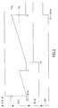
- FIG. 3 The basic diagram of a circuit according to the present invention is depicted in Fig. 3, while Figures 1 and 2 diagrammatically illustrate the algorithm of the invention for two different situations which may occur at the turn-on of the IC.
- both the soft start function and the power monitor function are implemented, according to the present invention, by using a single external capacitor C, thus requiring only one pin of the device.
- the capacitor C is charged by the current generator I towards a certain voltage, generically indicated as Vreg.
- the transistor Ml is biased in a conduction state thus maintaining discharged the external capacitor C.
- the block PULSE GEN Upon the rising of a first logic signal 5/12ok, asserting the application of the externally provided supply voltages to the device, the block PULSE GEN sets the register FF1, whose output Q is coupled to the control node of the transistor Ml, causing its turn-off.
- the PULSE GEN block besides setting the flip-flop FF1, resets the flip-flop FF2, whose output Q is coupled to an input of an AND gate the output of which is coupled to the control terminal of a second transistor M2 electrically connected in parallel to the capacitor C, keeping it in an off state.
- the external capacitor C starts charging towards Vreg with a constant current established by the charge current generator I.
- the voltage on the capacitor C is input to the block RAMP GEN which generates a direct replica and eventually a second replica of the charge ramp of the voltage on the capacitor C whose level is shifted and whose sign is inverted.
- the two ramps so generated namely: RAMP_RISE and RAMP_FALL, implement the "soft start" of the internal regulators.
- the initial soft start interval ends when on the external capacitor C a certain pre-established voltage of intermediate value is reached, typically the band-gap voltage Vbg.
- the generator RAMP GEN generates a first ramp RAMP_RISE, who is substantially a replica of the voltage ramp developing on the external capacitor C, starting from zero up to the value of the band-gap voltage Vbg, and a second ramp RAMP_FALL falling from a shifted level of 2*Vbg down to the Vbg level.
- the soft start interval ends when the voltage on the capacitor C attains the value Vbg, event which is sensed by the comparator COMP at the instant t 1 , whose output sets the second flip-flop FF2 with a minimum delay (t 1 + delay).
- the power monitor algorithm of the invention discriminates between two distinct situations that may occur at the instant t 1 or more precisely at the instant t 1 plus a minimum switching delay of the comparator COMP which establishes the end of the soft start ramp.
- a second signal DC_ok is produced in a conventional manner in the IC to assert or deny the condition that all the power supplies, that is the externally provided supply voltages (5V and 12V) and the internally generated supply voltages (3.3V, 2.5V and -5V), have a correct value.
- Such a second assertion signal (flag) DC_ok is applied to a first input of a NAND gate, to the second input of which is coupled to the output Q of the second flip-flop FF2.
- the output of the NAND gate is coupled to a second input of an inverting AND gate whose output controls the second transistor M2.
- the transistor M2 is kept in cut-off state, thus allowing the ramp charge of the capacitor C to continue until a second pre-established level is eventually reached, commonly a multiple of Vbg, in the example 2*Vbg.
- a second pre-established level commonly a multiple of Vbg, in the example 2*Vbg.
- Such second threshold is sufficiently high to cause the triggering of the Schmitt trigger ST whose output, by resetting the first flip-flop FF1, turns on the transistor M1 which immediately discharges the external capacitor C, ending the turn-on process and the enablement of the power monitor function by forcing the NPOR output to a high logic level.
- the block DEGLITCH has the function of masking undue transitions of the NPOR signal during the normal operation of the IC that could occur because of spurious switchings of the DC_ok signal of infinitesimal duration which may be caused by accidental transient phenomena, noise coming from the mains, etc.
- the output of the NAND gate is applied to an input of the block DEGLITCH, who discriminates the duration of eventual switchings from the high to low state of the signal DC_ok, in practice filtering out spurious switchings having a duration shorter than a minimum pre-established time interval.
- the capacitor is kept discharged until the signal DC_ok switches to a high logic level at the instant t 3 , which causes the turning-off of the transistor M2 and the start anew of the charge ramp on the external capacitor C.
- the stated objective is fully accomplished, being the soft start and power monitor requirements perfectly satisfied by the system of the invention, using a single external capacitor C.
Landscapes
- Physics & Mathematics (AREA)
- General Physics & Mathematics (AREA)
- Control Of Voltage And Current In General (AREA)
- Semiconductor Integrated Circuits (AREA)
Priority Applications (3)
| Application Number | Priority Date | Filing Date | Title |
|---|---|---|---|
| EP99830559A EP1083436B1 (fr) | 1999-09-08 | 1999-09-08 | Procédé et circuit de test de la présence de multiples tensions d'alimentations dans un circuit integré |
| DE69925593T DE69925593D1 (de) | 1999-09-08 | 1999-09-08 | Verfahren und Schaltungsanordnung zum Testen der Anwesenheit von mehreren Versorgungsspannungen in einer integrierten Schaltung |
| US09/657,436 US6320439B1 (en) | 1999-09-08 | 2000-09-07 | Method and circuit of soft start and of power monitor for IC with multiple supplies |
Applications Claiming Priority (1)
| Application Number | Priority Date | Filing Date | Title |
|---|---|---|---|
| EP99830559A EP1083436B1 (fr) | 1999-09-08 | 1999-09-08 | Procédé et circuit de test de la présence de multiples tensions d'alimentations dans un circuit integré |
Publications (2)
| Publication Number | Publication Date |
|---|---|
| EP1083436A1 true EP1083436A1 (fr) | 2001-03-14 |
| EP1083436B1 EP1083436B1 (fr) | 2005-06-01 |
Family
ID=8243574
Family Applications (1)
| Application Number | Title | Priority Date | Filing Date |
|---|---|---|---|
| EP99830559A Expired - Lifetime EP1083436B1 (fr) | 1999-09-08 | 1999-09-08 | Procédé et circuit de test de la présence de multiples tensions d'alimentations dans un circuit integré |
Country Status (3)
| Country | Link |
|---|---|
| US (1) | US6320439B1 (fr) |
| EP (1) | EP1083436B1 (fr) |
| DE (1) | DE69925593D1 (fr) |
Families Citing this family (5)
| Publication number | Priority date | Publication date | Assignee | Title |
|---|---|---|---|---|
| US6813170B2 (en) | 2002-08-19 | 2004-11-02 | Semtech Corporation | Multiple output power supply having soft start protection for load over-current or short circuit conditions |
| US8145934B1 (en) | 2009-07-31 | 2012-03-27 | Western Digital Technologies, Inc. | Soft start sequencer for starting multiple voltage regulators |
| US8692593B1 (en) * | 2012-09-14 | 2014-04-08 | Nxp B.V. | Zero or ultra-low DC current consumption power-on and brown-out detector |
| US10209279B2 (en) | 2015-06-24 | 2019-02-19 | Allegro Microsystems, Llc | Methods and apparatus for monitoring a level of a regulated source |
| CN111949060A (zh) * | 2020-08-14 | 2020-11-17 | 电子科技大学 | 一种缓启动电路 |
Citations (5)
| Publication number | Priority date | Publication date | Assignee | Title |
|---|---|---|---|---|
| US5063303A (en) * | 1991-02-08 | 1991-11-05 | Racal Data Communications Inc. | Soft start circuit |
| US5264782A (en) * | 1992-08-10 | 1993-11-23 | International Business Machines Corporation | Dropout recovery circuit |
| EP0709949A2 (fr) * | 1994-10-24 | 1996-05-01 | Telefonica De Espana, S.A. | Convertisseur continu-continu pour alimentation |
| US5710701A (en) * | 1995-07-31 | 1998-01-20 | Deli Usa, L.P. | Method and apparatus for power supply testing |
| EP0871037A1 (fr) * | 1997-04-07 | 1998-10-14 | Siemens Aktiengesellschaft | Dispositif pour surveiller un circuit électronique |
Family Cites Families (1)
| Publication number | Priority date | Publication date | Assignee | Title |
|---|---|---|---|---|
| FR2755317B1 (fr) * | 1996-10-25 | 1999-01-15 | Sgs Thomson Microelectronics | Regulateur de tension a generation interne d'un signal logique |
-
1999
- 1999-09-08 EP EP99830559A patent/EP1083436B1/fr not_active Expired - Lifetime
- 1999-09-08 DE DE69925593T patent/DE69925593D1/de not_active Expired - Lifetime
-
2000
- 2000-09-07 US US09/657,436 patent/US6320439B1/en not_active Expired - Lifetime
Patent Citations (5)
| Publication number | Priority date | Publication date | Assignee | Title |
|---|---|---|---|---|
| US5063303A (en) * | 1991-02-08 | 1991-11-05 | Racal Data Communications Inc. | Soft start circuit |
| US5264782A (en) * | 1992-08-10 | 1993-11-23 | International Business Machines Corporation | Dropout recovery circuit |
| EP0709949A2 (fr) * | 1994-10-24 | 1996-05-01 | Telefonica De Espana, S.A. | Convertisseur continu-continu pour alimentation |
| US5710701A (en) * | 1995-07-31 | 1998-01-20 | Deli Usa, L.P. | Method and apparatus for power supply testing |
| EP0871037A1 (fr) * | 1997-04-07 | 1998-10-14 | Siemens Aktiengesellschaft | Dispositif pour surveiller un circuit électronique |
Also Published As
| Publication number | Publication date |
|---|---|
| DE69925593D1 (de) | 2005-07-07 |
| US6320439B1 (en) | 2001-11-20 |
| EP1083436B1 (fr) | 2005-06-01 |
Similar Documents
| Publication | Publication Date | Title |
|---|---|---|
| US4788462A (en) | Power-On-Reset (POR) circuit | |
| JP4540610B2 (ja) | 半導体集積回路装置及びそれを用いた電源電圧監視システム | |
| US11114880B2 (en) | Current regulating circuit and power supply management circuit including the same | |
| US7141958B2 (en) | Power supply apparatus and power supply control device | |
| US5426776A (en) | Microprocessor watchdog circuit | |
| US20050127984A1 (en) | Power supply circuit having a plurality of voltage conversion circuits | |
| EP1083436B1 (fr) | Procédé et circuit de test de la présence de multiples tensions d'alimentations dans un circuit integré | |
| CN217469914U (zh) | 上电复位电路 | |
| US20040217785A1 (en) | Reset circuits | |
| KR100662689B1 (ko) | 히스테리시스 콤퍼레이터 및 그것을 이용한 리세트 신호발생 회로 | |
| CN115149499B (zh) | 电子保护装置及其控制方法、芯片及电子设备 | |
| JPH01258459A (ja) | 電池を電源とした集積回路 | |
| US5818206A (en) | Method and apparatus for automatically detecting device specifications and providing a corresponding operating voltage | |
| US11563430B2 (en) | Transistor diagnostic circuit | |
| US6661263B2 (en) | Voltage sequencing arrangements providing first and second voltages sequenced to each other in time | |
| US7501716B2 (en) | Power supply apparatus | |
| KR100345956B1 (ko) | 강제동작기능 부착의 제어장치 및 반도체 집적회로장치 | |
| JP2003223229A (ja) | 安定化電源装置およびそれを用いた電子機器 | |
| JP2025079596A (ja) | 半導体集積回路及び電子機器 | |
| JP2022182787A (ja) | 立ち上がり遅延回路 | |
| CN111900783B (zh) | 过功率保护电路、充电器及过功率保护方法 | |
| JPH03198622A (ja) | システムリセット回路 | |
| JPH06209567A (ja) | Dc/dcコンバータの突入電流防止回路 | |
| JP2879845B2 (ja) | 半導体装置 | |
| WO2025094354A1 (fr) | Circuit électrique et appareil électronique |
Legal Events
| Date | Code | Title | Description |
|---|---|---|---|
| PUAI | Public reference made under article 153(3) epc to a published international application that has entered the european phase |
Free format text: ORIGINAL CODE: 0009012 |
|
| AK | Designated contracting states |
Kind code of ref document: A1 Designated state(s): DE FR GB IT |
|
| AX | Request for extension of the european patent |
Free format text: AL;LT;LV;MK;RO;SI |
|
| 17P | Request for examination filed |
Effective date: 20010807 |
|
| AKX | Designation fees paid |
Free format text: DE FR GB IT |
|
| GRAP | Despatch of communication of intention to grant a patent |
Free format text: ORIGINAL CODE: EPIDOSNIGR1 |
|
| GRAS | Grant fee paid |
Free format text: ORIGINAL CODE: EPIDOSNIGR3 |
|
| GRAA | (expected) grant |
Free format text: ORIGINAL CODE: 0009210 |
|
| AK | Designated contracting states |
Kind code of ref document: B1 Designated state(s): DE FR GB IT |
|
| REG | Reference to a national code |
Ref country code: GB Ref legal event code: FG4D |
|
| REF | Corresponds to: |
Ref document number: 69925593 Country of ref document: DE Date of ref document: 20050707 Kind code of ref document: P |
|
| PG25 | Lapsed in a contracting state [announced via postgrant information from national office to epo] |
Ref country code: DE Free format text: LAPSE BECAUSE OF FAILURE TO SUBMIT A TRANSLATION OF THE DESCRIPTION OR TO PAY THE FEE WITHIN THE PRESCRIBED TIME-LIMIT Effective date: 20050902 |
|
| PLBE | No opposition filed within time limit |
Free format text: ORIGINAL CODE: 0009261 |
|
| STAA | Information on the status of an ep patent application or granted ep patent |
Free format text: STATUS: NO OPPOSITION FILED WITHIN TIME LIMIT |
|
| 26N | No opposition filed |
Effective date: 20060302 |
|
| EN | Fr: translation not filed | ||
| PGFP | Annual fee paid to national office [announced via postgrant information from national office to epo] |
Ref country code: IT Payment date: 20070913 Year of fee payment: 9 |
|
| PG25 | Lapsed in a contracting state [announced via postgrant information from national office to epo] |
Ref country code: FR Free format text: LAPSE BECAUSE OF NON-PAYMENT OF DUE FEES Effective date: 20050930 |
|
| PG25 | Lapsed in a contracting state [announced via postgrant information from national office to epo] |
Ref country code: FR Free format text: LAPSE BECAUSE OF NON-PAYMENT OF DUE FEES Effective date: 20050601 |
|
| PG25 | Lapsed in a contracting state [announced via postgrant information from national office to epo] |
Ref country code: IT Free format text: LAPSE BECAUSE OF NON-PAYMENT OF DUE FEES Effective date: 20080908 |
|
| PGFP | Annual fee paid to national office [announced via postgrant information from national office to epo] |
Ref country code: GB Payment date: 20100826 Year of fee payment: 12 |
|
| GBPC | Gb: european patent ceased through non-payment of renewal fee |
Effective date: 20110908 |
|
| PG25 | Lapsed in a contracting state [announced via postgrant information from national office to epo] |
Ref country code: GB Free format text: LAPSE BECAUSE OF NON-PAYMENT OF DUE FEES Effective date: 20110908 |