EP1085583A2 - Halbleiteranordnungen mit Quantenwelleninterferenzschichten - Google Patents
Halbleiteranordnungen mit Quantenwelleninterferenzschichten Download PDFInfo
- Publication number
- EP1085583A2 EP1085583A2 EP00118585A EP00118585A EP1085583A2 EP 1085583 A2 EP1085583 A2 EP 1085583A2 EP 00118585 A EP00118585 A EP 00118585A EP 00118585 A EP00118585 A EP 00118585A EP 1085583 A2 EP1085583 A2 EP 1085583A2
- Authority
- EP
- European Patent Office
- Prior art keywords
- layer
- quantum
- layers
- wave
- wave interference
- Prior art date
- Legal status (The legal status is an assumption and is not a legal conclusion. Google has not performed a legal analysis and makes no representation as to the accuracy of the status listed.)
- Withdrawn
Links
- 239000004065 semiconductor Substances 0.000 title claims description 33
- 238000005253 cladding Methods 0.000 claims abstract description 29
- 125000005842 heteroatom Chemical group 0.000 claims abstract description 5
- 239000000969 carrier Substances 0.000 claims description 75
- 230000005540 biological transmission Effects 0.000 claims description 34
- 238000005381 potential energy Methods 0.000 claims description 16
- 230000000694 effects Effects 0.000 claims description 7
- 230000005669 field effect Effects 0.000 claims description 6
- 230000005641 tunneling Effects 0.000 claims description 3
- 229910001218 Gallium arsenide Inorganic materials 0.000 abstract description 18
- 230000004888 barrier function Effects 0.000 abstract description 4
- 238000002310 reflectometry Methods 0.000 description 8
- 239000000758 substrate Substances 0.000 description 8
- 239000010931 gold Substances 0.000 description 6
- 230000000644 propagated effect Effects 0.000 description 6
- 238000010586 diagram Methods 0.000 description 5
- JBRZTFJDHDCESZ-UHFFFAOYSA-N AsGa Chemical compound [As]#[Ga] JBRZTFJDHDCESZ-UHFFFAOYSA-N 0.000 description 4
- 229910052782 aluminium Inorganic materials 0.000 description 3
- 229910052733 gallium Inorganic materials 0.000 description 3
- GYHNNYVSQQEPJS-UHFFFAOYSA-N Gallium Chemical compound [Ga] GYHNNYVSQQEPJS-UHFFFAOYSA-N 0.000 description 2
- XAGFODPZIPBFFR-UHFFFAOYSA-N aluminium Chemical compound [Al] XAGFODPZIPBFFR-UHFFFAOYSA-N 0.000 description 2
- 239000013065 commercial product Substances 0.000 description 2
- 238000000151 deposition Methods 0.000 description 2
- 230000008021 deposition Effects 0.000 description 2
- -1 gallium arsenide (GaAs) compound Chemical group 0.000 description 2
- 229910052732 germanium Inorganic materials 0.000 description 2
- GNPVGFCGXDBREM-UHFFFAOYSA-N germanium atom Chemical compound [Ge] GNPVGFCGXDBREM-UHFFFAOYSA-N 0.000 description 2
- PCHJSUWPFVWCPO-UHFFFAOYSA-N gold Chemical compound [Au] PCHJSUWPFVWCPO-UHFFFAOYSA-N 0.000 description 2
- 229910052737 gold Inorganic materials 0.000 description 2
- 229910021478 group 5 element Inorganic materials 0.000 description 2
- 229910052738 indium Inorganic materials 0.000 description 2
- 230000006698 induction Effects 0.000 description 2
- 238000000034 method Methods 0.000 description 2
- 230000004048 modification Effects 0.000 description 2
- 238000012986 modification Methods 0.000 description 2
- 230000003287 optical effect Effects 0.000 description 2
- 238000005036 potential barrier Methods 0.000 description 2
- 230000001902 propagating effect Effects 0.000 description 2
- 230000004044 response Effects 0.000 description 2
- 239000007787 solid Substances 0.000 description 2
- 230000003321 amplification Effects 0.000 description 1
- 229910052787 antimony Inorganic materials 0.000 description 1
- RBFQJDQYXXHULB-UHFFFAOYSA-N arsane Chemical compound [AsH3] RBFQJDQYXXHULB-UHFFFAOYSA-N 0.000 description 1
- 229910052785 arsenic Inorganic materials 0.000 description 1
- RQNWIZPPADIBDY-UHFFFAOYSA-N arsenic atom Chemical compound [As] RQNWIZPPADIBDY-UHFFFAOYSA-N 0.000 description 1
- 229910000070 arsenic hydride Inorganic materials 0.000 description 1
- 230000003542 behavioural effect Effects 0.000 description 1
- 230000008901 benefit Effects 0.000 description 1
- 229910052797 bismuth Inorganic materials 0.000 description 1
- 229910052796 boron Inorganic materials 0.000 description 1
- 238000006243 chemical reaction Methods 0.000 description 1
- 238000005229 chemical vapour deposition Methods 0.000 description 1
- 150000001875 compounds Chemical class 0.000 description 1
- 230000008878 coupling Effects 0.000 description 1
- 238000010168 coupling process Methods 0.000 description 1
- 238000005859 coupling reaction Methods 0.000 description 1
- 238000000354 decomposition reaction Methods 0.000 description 1
- 239000002019 doping agent Substances 0.000 description 1
- 238000002474 experimental method Methods 0.000 description 1
- BHEPBYXIRTUNPN-UHFFFAOYSA-N hydridophosphorus(.) (triplet) Chemical compound [PH] BHEPBYXIRTUNPN-UHFFFAOYSA-N 0.000 description 1
- 230000006872 improvement Effects 0.000 description 1
- 239000012535 impurity Substances 0.000 description 1
- APFVFJFRJDLVQX-UHFFFAOYSA-N indium atom Chemical compound [In] APFVFJFRJDLVQX-UHFFFAOYSA-N 0.000 description 1
- 239000000463 material Substances 0.000 description 1
- 229910052751 metal Inorganic materials 0.000 description 1
- 239000002184 metal Substances 0.000 description 1
- 229910052757 nitrogen Inorganic materials 0.000 description 1
- 238000003199 nucleic acid amplification method Methods 0.000 description 1
- 239000002245 particle Substances 0.000 description 1
- 229910052698 phosphorus Inorganic materials 0.000 description 1
- 230000000630 rising effect Effects 0.000 description 1
- 229910052716 thallium Inorganic materials 0.000 description 1
Images





Classifications
-
- H—ELECTRICITY
- H10—SEMICONDUCTOR DEVICES; ELECTRIC SOLID-STATE DEVICES NOT OTHERWISE PROVIDED FOR
- H10H—INORGANIC LIGHT-EMITTING SEMICONDUCTOR DEVICES HAVING POTENTIAL BARRIERS
- H10H20/00—Individual inorganic light-emitting semiconductor devices having potential barriers, e.g. light-emitting diodes [LED]
- H10H20/80—Constructional details
- H10H20/81—Bodies
- H10H20/814—Bodies having reflecting means, e.g. semiconductor Bragg reflectors
-
- H—ELECTRICITY
- H10—SEMICONDUCTOR DEVICES; ELECTRIC SOLID-STATE DEVICES NOT OTHERWISE PROVIDED FOR
- H10F—INORGANIC SEMICONDUCTOR DEVICES SENSITIVE TO INFRARED RADIATION, LIGHT, ELECTROMAGNETIC RADIATION OF SHORTER WAVELENGTH OR CORPUSCULAR RADIATION
- H10F77/00—Constructional details of devices covered by this subclass
- H10F77/40—Optical elements or arrangements
- H10F77/413—Optical elements or arrangements directly associated or integrated with the devices, e.g. back reflectors
-
- H—ELECTRICITY
- H10—SEMICONDUCTOR DEVICES; ELECTRIC SOLID-STATE DEVICES NOT OTHERWISE PROVIDED FOR
- H10H—INORGANIC LIGHT-EMITTING SEMICONDUCTOR DEVICES HAVING POTENTIAL BARRIERS
- H10H20/00—Individual inorganic light-emitting semiconductor devices having potential barriers, e.g. light-emitting diodes [LED]
- H10H20/80—Constructional details
- H10H20/81—Bodies
- H10H20/816—Bodies having carrier transport control structures, e.g. highly-doped semiconductor layers or current-blocking structures
-
- H—ELECTRICITY
- H01—ELECTRIC ELEMENTS
- H01S—DEVICES USING THE PROCESS OF LIGHT AMPLIFICATION BY STIMULATED EMISSION OF RADIATION [LASER] TO AMPLIFY OR GENERATE LIGHT; DEVICES USING STIMULATED EMISSION OF ELECTROMAGNETIC RADIATION IN WAVE RANGES OTHER THAN OPTICAL
- H01S5/00—Semiconductor lasers
- H01S5/20—Structure or shape of the semiconductor body to guide the optical wave ; Confining structures perpendicular to the optical axis, e.g. index or gain guiding, stripe geometry, broad area lasers, gain tailoring, transverse or lateral reflectors, special cladding structures, MQW barrier reflection layers
- H01S5/2004—Confining in the direction perpendicular to the layer structure
-
- H—ELECTRICITY
- H01—ELECTRIC ELEMENTS
- H01S—DEVICES USING THE PROCESS OF LIGHT AMPLIFICATION BY STIMULATED EMISSION OF RADIATION [LASER] TO AMPLIFY OR GENERATE LIGHT; DEVICES USING STIMULATED EMISSION OF ELECTROMAGNETIC RADIATION IN WAVE RANGES OTHER THAN OPTICAL
- H01S5/00—Semiconductor lasers
- H01S5/20—Structure or shape of the semiconductor body to guide the optical wave ; Confining structures perpendicular to the optical axis, e.g. index or gain guiding, stripe geometry, broad area lasers, gain tailoring, transverse or lateral reflectors, special cladding structures, MQW barrier reflection layers
- H01S5/2004—Confining in the direction perpendicular to the layer structure
- H01S5/2009—Confining in the direction perpendicular to the layer structure by using electron barrier layers
-
- H—ELECTRICITY
- H01—ELECTRIC ELEMENTS
- H01S—DEVICES USING THE PROCESS OF LIGHT AMPLIFICATION BY STIMULATED EMISSION OF RADIATION [LASER] TO AMPLIFY OR GENERATE LIGHT; DEVICES USING STIMULATED EMISSION OF ELECTROMAGNETIC RADIATION IN WAVE RANGES OTHER THAN OPTICAL
- H01S5/00—Semiconductor lasers
- H01S5/20—Structure or shape of the semiconductor body to guide the optical wave ; Confining structures perpendicular to the optical axis, e.g. index or gain guiding, stripe geometry, broad area lasers, gain tailoring, transverse or lateral reflectors, special cladding structures, MQW barrier reflection layers
- H01S5/2004—Confining in the direction perpendicular to the layer structure
- H01S5/2009—Confining in the direction perpendicular to the layer structure by using electron barrier layers
- H01S5/2013—MQW barrier reflection layers
-
- Y—GENERAL TAGGING OF NEW TECHNOLOGICAL DEVELOPMENTS; GENERAL TAGGING OF CROSS-SECTIONAL TECHNOLOGIES SPANNING OVER SEVERAL SECTIONS OF THE IPC; TECHNICAL SUBJECTS COVERED BY FORMER USPC CROSS-REFERENCE ART COLLECTIONS [XRACs] AND DIGESTS
- Y02—TECHNOLOGIES OR APPLICATIONS FOR MITIGATION OR ADAPTATION AGAINST CLIMATE CHANGE
- Y02E—REDUCTION OF GREENHOUSE GAS [GHG] EMISSIONS, RELATED TO ENERGY GENERATION, TRANSMISSION OR DISTRIBUTION
- Y02E10/00—Energy generation through renewable energy sources
- Y02E10/50—Photovoltaic [PV] energy
- Y02E10/547—Monocrystalline silicon PV cells
Definitions
- the present invention relates to a gallium arsenide (GaAs) compound group semiconductor device having quantum-wave interference layers which reflect carriers, i.e., electrons or holes, effectively.
- the present invention also relates to a gallium arsenide (GaAs) semiconductor device having quantum-wave interference layers which transmit carriers, i.e., electrons or holes, effectively.
- the present invention relates to a light-emitting device such as a laser or a light-emitting diode with a structure which confines carriers in an active layer so as to improve its luminous efficiency.
- a semiconductor device has been known to have a double hetero junction structure whose active layer is formed between n-type and p-type cladding layers.
- the cladding layers function as potential barriers for effectively confining carriers, or electrons and holes, within the active layer.
- the inventor of the present invention conducted a series of experiments and found that, although it can be understood that Takagi et al. used a band gap energy alternative to a kinetic energy, the suggested thickness of the first and the second layers by Takagi et al. were too small to confine electrons, and that preferable thicknesses of the first and second layers are 4 to 6 times larger than those suggested by Takagi et al. So a problem still persisted in inadequacy of reflecting carriers.
- the inventor of the present invention concerned a characteristic of electrons as a wave and considered that the quantum-wave interference layer functions as a transmission layer of carriers, by analogy with the multiple reflection of the light. That is, when each thickness of layers in the multiple layer structure is about an order of the wavelength of a quantum-wave of carriers, an interference effect of quantum-wave is considered to occur with respect to a conduction of carriers in the multiple layer structure.
- the interference effect caused a conduction as a wave.
- the inventor of the present invention considered that not a conduction of particle in a classical theory but a resonance of waves, an interference, or other phenomenon is occurred by an interference effect of electrons. This wave behavioral characteristic of electrons improves a mobility and a propagation velocity.
- a first object of the present invention is to provide a semiconductor device with a new structure, having a quantum-wave interference layer with a large reflectivity to carriers which functions as a reflection layer or a quantum-wave interference layer with a high transmittivity and a high mobility to carriers which functions as a transmission layer.
- a first characteristic group of this invention is described as follows.
- a first aspect of the present invention is a semiconductor device constituted by a quantum-wave interference layer having plural periods of a pair of a first layer made of Al x Ga 1-x As and a second layer made of Al y Ga 1-y As (0 ⁇ x ⁇ y ⁇ 1), the second layer having a wider band gap than the first layer.
- Each thickness of the first and the second layers is determined by multiplying by an odd number one fourth of a quantum-wave wavelength of carriers in each of the first and the second layers.
- a second aspect of the present invention is to form each thickness of the first and the second layers by multiplying by an odd number one fourth of quantum-wave wavelength of carriers in each of the first and the second layers existing at the level near the lowest energy level of the second layer.
- h, m RW , m RB , E R , V R , and n RW , n RB represent Plank's constant, the effective mass of carriers in the first layer, the effective mass of carriers in the second layer, the kinetic energy of the carriers at the level near the lowest energy level of the second layer, the potential energy of the second layer relative to the first layer, and odd numbers, respectively.
- Carriers injected into the second layer are preferably existing around the lowest energy of the second layer.
- a fourth aspect of the present invention is the first quantum-wave interference layer having a plurality of partial quantum-wave interference layers I Rk with arbitrary periods T Rk including a first layer having a thickness of D RWk and a second layer having a thickness of D RBk and arranged in series.
- E Rk , m RWk , m RBk , and n RWk , n RBk represent plural kinetic energy levels of carriers flowing into the second layer, effective mass of carriers with kinetic energy E Rk +V R in the first layer, effective mass of carriers with kinetic energy E Rk in the second layer, and arbitrary odd numbers, respectively.
- the plurality of the partial quantum-wave interference layers I Rk are arranged in series from I R1 to I Rj , where j is a maximum number of k required to from a quantum-wave interference layer as a whole.
- a fifth aspect of the present invention is a semiconductor device having a first quantum-wave interference layer with a plurality of partial quantum-wave interference layers arranged in series with arbitrary periods.
- Each of the plurality of partial quantum-wave interference layers is constructed with serial pairs of the first and second layers.
- the widths of the first and second layers of the serial parts are represented by (D RB1 , D RW1 ), ..., (D RBk , D RWk ), ..., (D RBj , D RWj ).
- (D RBk , D RWk ) is a pair of widths of the first and second layers and is defined as Eqs 2-1 and 2-2, respectively.
- a sixth aspect of the present invention is to form a ⁇ R layer, which varies an energy band sharply, at an interface between the first and the second layers.
- a thickness of the ⁇ R layer is substantially thinner than that of the first and the second layers.
- a seventh aspect of the present invention is to provide a quantum-wave interference layer which functions as a reflection layer of carriers.
- An eighth aspect of the present invention is to constitute a quantum-wave incident facet in the quantum-wave interference layer by a second layer with enough thickness for preventing conduction of carriers by a tunneling effect.
- Ninth to fifteenth aspects of the present invention in a second characteristic group correspond to the first to seventh aspects of the present invention in the first characteristic group, respectively.
- a quantum-wave interference layer (second kind) shown in the second characteristic group has a different structure from that of the quantum-wave interference layer (first kind) shown in the first characteristic group. While the first kind of quantum-wave interference layer has a first layer and a second layer, each thickness of which is determined by multiplying by an odd number one fourth of a quantum-wave wavelength of carriers in each of the first and the second layers, the second kind of quantum-wave interference layer has a first layer and a second layer, each thickness of which is determined by multiplying by an even number one fourth of a quantum-wave wavelength of carriers in each of the first and the second layers.
- a ninth aspect of the present invention which corresponds to the first aspect of the present invention, is a semiconductor device constituted by a quantum-wave interference layer having plural periods of a pair of a first layer made of Al x Ga 1-x As and a second layer made of Al y Ga 1-y As (0 ⁇ x ⁇ y ⁇ 1), the second layer having a wider band gap than the first layer.
- Each thickness of the first and the second layers is determined by multiplying by an even number one fourth of a quantum-wave wavelength of carriers in each of the first and the second layers.
- a tenth aspect of the present invention which corresponds to the second aspect of the present invention, is to form each thickness of the first and the second layers by multiplying by an even number one fourth of quantum-wave wavelength of carriers in each of the first and the second layers existing at the level near the lowest energy level of the second layer.
- h, m TW , m TB , E T , V T , and n TW , n TB represent Plank's constant, the effective mass of carriers in the first layer, the effective mass of carriers in the second layer, the kinetic energy of the carriers at the level near the lowest energy level of the second layer, the potential energy of the second layer relative to the first layer, and even numbers, respectively.
- Carriers injected into the second layer are preferably existing around the lowest energy of the second layer.
- a twelfth aspect of the present invention which corresponds to the fourth aspect of the present invention, is a quantum-wave interference layer having a plurality of partial quantum-wave interference layers I Tk with arbitrary periods T Tk including a first layer having a thickness of D TWk and a second layer having a thickness of D TBk and arranged in series.
- E Tk , m TWk , m TBk , and n TWk , n TBk represent plural kinetic energy levels of carriers flowing into the second layer, effective mass of carriers with kinetic energy E Tk +V T in the first layer, effective mass of carriers with kinetic energy E Tk in the second layer, and arbitrary even numbers, respectively.
- the plurality of the partial quantum-wave interference layers I Tk are arranged in series from I T1 to I Tj , where j is a maximum number of k required to from a quantum-wave interference layer as a whole.
- a thirteenth aspect of the present invention which corresponds to the fifth aspect of the present invention, is a semiconductor device having a quantum-wave interference layer with a plurality of partial quantum-wave interference layers arranged in series with arbitrary periods.
- Each of the plurality of partial quantum-wave interference layers is constructed with serial pairs of the first and second layers.
- the widths of the first and second layers of the serial parts are represented by (D TB1 , D TW1 ), ..., (D TBk , D TWk ), ..., (D TBj , D TWj ).
- (D TBk , D TWk ) is a pair of widths of the first and second layers and is defined as Eqs 4-1 and 4-2, respectively.
- a fourteenth aspect of the present invention which corresponds to the sixth aspect of the present invention, is to form a ⁇ T layer, which varies an energy band sharply, at an interface between the first and the second layers.
- a thickness of the ⁇ T layer is substantially thinner than that of the first and the second layers.
- a fifteenth aspect of the present invention which corresponds to the seventh aspect of the present invention, is to provide a quantum-wave interference layer which functions as a transmission layer of carriers.
- a sixteenth aspect of the present invention is a semiconductor device constituted by an n-type layer, a p-type layer, and an active layer that is formed between the n-type layer and the p-type layer, and wherein at least one of the n-type layer and the p-type layer is at least one or both of two kinds of the quantum-wave interference layer, i.e., reflection type ( ⁇ /4) and transmission type ( ⁇ /2).
- Carriers, or electrons and holes to reflect or transmit can be selected arbitrary and corresponding two kinds of quantum-wave interference layer may be used for electrons and holes. Two kinds of quantum-wave interference layer may be used at the same time for either one of electrons and holes, alternatively, for both of electrons and holes.
- a seventeenth aspect of the present invention is to provide a light-emitting device having the quantum-wave interference layer in at least one of an n-type cladding layer and a p-type cladding layer.
- the quantum-wave interference layer which functions as a reflection layer, is used.
- An eighteenth aspect of the present invention is a field effect transistor including the quantum-wave interference layer which is described in the first or the second characteristic groups of the present invention. That is, at least one of the reflection-type and the transmission-type quantum-wave interference layers is formed positioned adjacent to a channel.
- a nineteenth aspect of the present invention is a photovoltaic device having a pn junction structure including an n-layer and a p-layer. At least one of the n-layer and the p-layer is made of the reflection-type quantum-wave interference layer for reflecting minor carriers.
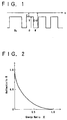
- FIG. 1 shows a conduction band of a multiple layer structure with plural periods of a first layer W and a second layer B as a unit.
- a band gap of the second layer B is wider than that of the first layer W.
- Electrons conduct from left to right as shown by an arrow in FIG. 1. Among the electrons, those that exist at the level near the lowest energy level of a conduction band in the second layer B are most likely to contribute to conduction.
- the electrons near the bottom of conduction band of the second layer B has a kinetic energy E.
- the electrons in the first layer W have a kinetic energy E+V which is accelerated by potential energy V due to the band gap between the first layer W and the second layer B.
- electrons that move from the first layer W to the second layer B are decelerated by potential energy V and return to the original kinetic energy E in the second layer B.
- kinetic energy of electrons in the conduction band is modulated by potential energy due to the multiple layer structure.
- the wave length of the electron quantum-wave is calculated by Eqs. 1-1 and 1-2 using kinetic energy of the electron.
- the kinetic energy E of the conducting electrons in the second layer B exists near the bottom of the conduction band, the relation of Eq. 9 is satisfied and the reflectivity R at the interface between the second layer B and the first layer W becomes 52 % or more. Consequently, the multiple quantum well layer structure can reflect quantum wave of electrons effectively.
- Thicknesses of the first layer W and the second layer B are determined for selectively transmitting one of holes and electrons, because of a difference in potential energy between the valence and the conduction bands, and a difference in effective mass of holes and electrons in the first layer W and the second layer B.
- the optimum thickness of the first and the second layers for reflecting electrons is not optimum for reflecting holes.
- Eqs. 1-1 and 1-2 refer to a structure of the quantum-wave interference layer for reflecting electrons selectively. The thickness for selectively reflecting electrons is designed based on a difference in potential energy of the conduction band and effective mass of electrons. Consequently, the quantum-wave interference layer has a high reflectivity for electrons, but not for holes.
- the thickness for selectively reflecting holes is designed based on a difference in potential energy of the valence band and effective mass of holes, realizing another type of quantum-wave interference layer which can reflect holes and transmits electrons.
- the principle of the second kinds of quantum-wave interference layer in the second characteristic group of the present invention is explained hereinafter.
- a quantum-wave wavelength for example, a half of a quantum-wave wavelength
- a standing wave rises in a quantum-wave interference layer, and a resonant conduction is occurred. That is, when a quantum-wave period of the standing wave and a potential period of the quantum-wave interference layer is corresponded to each other, a scattering of the carrier in each layer is suppressed, and a conduction of a high mobility is realized.
- Thicknesses of the first layer W and the second layer B are determined for selectively transmitting one of holes and electrons, because of a difference in potential energy between the valence and the conduction bands, and a difference in effective mass of holes and electrons in the first layer W and the second layer B.
- the optimum thickness of the first and the second layers for transmitting electrons is not optimum for transmitting holes.
- Eqs. 3-1 and 3-2 refer to a structure of the quantum-wave interference layer for transmitting electrons selectively. The thickness for selectively transmitting electrons is designed based on a difference in potential energy of the conduction band and effective mass of electrons. Consequently, the quantum-wave interference layer has a high transmittivity (or a high mobility) for electrons, but not for holes.
- the thickness for selectively transmitting holes is designed based on a difference in potential energy of the valence band and effective mass of holes, realizing another type of quantum-wave interference layer as a hole transmission layer, which has a high mobility for holes and which has an ordinary mobility for electrons.
- FIGS. 3A-3H illustrate the relationship between reflection of quantum-wave of electrons in a potential of quantum-well structure and a period of potential representing a conduction band of a multiple quantum well (MQW).
- FIGS. 3A-3D show the relationship when the period, i.e., width of the second layer B or the first layer W, of the potential is equal to an odd number multiplied by one fourth of the wavelength of propagated election quantum-wave. This type of the potential is named as ⁇ /4 type potential hereinafter.
- FIGS. 3E-3H show when the period of the potential is equal to a natural number multiplied by a half of the wavelength of propagated electron quantum-wave.
- FIGS. 3A-3H Electrons existing around the bottom of a conduction band of the second layer B conduct from left to right as shown by an arrow in FIGS. 3A and 3E. And in FIGS. 3B and 3F, the electrons reach the interface between the first layer W and the second layer B.
- the propagating quantum-wave of electrons represented by QW1, QW2 and QW4 and the reflecting quantum-wave of electrons represented by QW3 and QW5 cancels with each other, as shown in FIG. 3D.
- the quantum-wave of electrons represented by the QW1, QW2 and QW4 propagates from left to right, and the quantum-wave of electrons represented by the QW3 and QW5, generated by the reflection at two interfaces, propagates from right to left.
- a multiple quantum well having a potential which is formed in a period, i.e., the width of the first layer W and the second layer B, determined by multiplying by an odd number one fourth of quantum-wave wavelength of propagated electrons, cancels the quantum-wave of electrons.
- the multiple quantum well functions as a reflection layer which does not propagate electrons.
- the quantum-wave of electrons can become a standing wave.
- a transmission wave QW2 and a reflection wave QW3 having a phase corresponding to that of the transmission wave QW2 are generated with respect to an incident wave QW1 as shown in FIG. 3G.
- a transmission wave QW4 and a reflection wave QW5 having a phase opposite to that of the transmission wave QW4 are generated as shown in FIG. 3H.
- the propagating quantum-wave of electrons represented by QW1, QW2 and QW4 and the reflecting quantum-wave of electrons represented by QW5 intensifies to each other, as shown in FIG. 3H.
- the reflection waves QW3 and QW5 can be considered to cancel with each other and the quantum-wave of electrons which is propagated from left to right in FIG. 3E can be a standing wave.
- the quantum-wave of electrons can become a standing wave and a transmission layer having a high transmittivity (or a high mobility) for electrons can be realized.
- a multiple quantum well having a potential which is formed in a period determined by multiplying by a natural number half of quantum-wave wavelength of holes, can be applied to the relationship described above.
- a semiconductor device in which both quantum-wave interference layers for electrons and holes in the first and the second characteristic groups, i.e., reflection-type and transmission-type, respectively, are formed as described above is obtained.
- electrons or holes are injected from the second kinds of quantum-wave interference layer, i.e., transmission-type, to the first kinds of quantum-wave interference layer, i.e., reflection-type, electrons or holes, which are not interrupted and flows with a high transmittivity in the second kind of quantum-wave interference layer, reach the first quantum-wave interference layer and are reflected effectively.
- carriers electros or holes
- a main part to drive the device can be formed between the second and the first kinds of quantum-wave interference layers.
- a plurality of partial quantum-wave interference layers I Rk as a quantum-wave interference layer may be formed corresponding to each of a plurality of kinetic energy levels E Rk .
- Each of the partial quantum-wave interference layers I Rk has T Rk periods of a first layer W and a second layer B as a unit whose respective thicknesses (D RWk , D RBk ) are determined by Eqs. 2-1 and 2-2.
- the plurality of the partial quantum-wave interference layer I Rk is arranged in series with respect to the number k of kinetic energy levels E Rk . That is, the quantum-wave interference layer is formed by a serial connection of I R1 , I R2 , ..., and I Rj . As shown in FIG.
- Each of the partial quantum-wave interference layers I Tk has T Tk periods of a first layer W and a second layer B as a unit whose respective thicknesses (D TWk , D TBk ) are determined by Eqs. 4-1 and 4-2.
- the plurality of the partial quantum-wave interference layer I Tk is arranged in series with respect to the number k of kinetic energy levels E Tk . That is, the quantum-wave interference layer is formed by a serial connection of I T1 , I T2 , ..., and I Tj .
- This quantum-wave interference layer becomes to have a high transmittivity (or a high mobility) with carriers.
- (D RWk , D RBk ), I Rk , and T Rk are not distinguished from (D TWk , D TBk ), I Tk , and T Tk , respectively, and each of them is represented by D Wk , D Bk , I k and T k .
- a plurality of partial quantum-wave interference layers as a quantum-wave interference layer may be formed with an arbitrary period.
- Each of the partial quantum-wave interference layers I R1 , I R2 , ... is made of serial pairs of the first layer W and the second layer B with widths (D RWk , D RBk ) determined by Eqs. 2-1 and 2-2. That is, the partial quantum-wave interference layer, e.g., I R1 , is constructed with serial layers of width (D RW1 , D RB1 ), ..., (D RWk , D RBk ), ..., (D RWj , D RBj ).
- the partial quantum-wave interference layer is constructed with serial layers of width (D TW1 , D TB1 ), ..., (D TWk , D TBk ), ..., (D TWj , D TBj ).
- This quantum-wave interference layer becomes to have a high transmittivity (or a high mobility) with carriers.
- (D RWk , D RBk ), I Rk , and T Rk are not distinguished from (D TWk , D TBk ), I Tk , and T Tk , respectively, and each of them is represented by D Wk , D Bk , I k and T k .
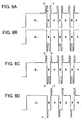
- FIGS. 6A-6D illustrate to form a ⁇ R layer (disclosed as a ⁇ layer in FIGS. 6A-6D) at the interface between the first layer W and the second layer B.
- the ⁇ R layer has a relatively thinner thickness than both of the first layer W and the second layer B and sharply varies an energy band.
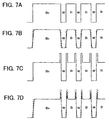
- the potential energy V of an energy band becomes larger substantially and the value x of Eq. 7 becomes smaller, as shown in FIGS. 6A-6D. This is shown in FIGS. 7A-7D.
- FIGS. 7A-7D Without forming a ⁇ R layer as shown in FIG.
- the ⁇ R layer may be formed on both ends of the every first layer W as shown in FIGS. 6A to 6D.
- the ⁇ R layers are formed so that an energy level higher than that of the second layer B may be formed.
- the ⁇ R layers are formed so that a band having lower bottom than that of the first layer W may be formed.
- the ⁇ R layers are formed so that the energy level higher than that of the second layer B and the energy level lower than that of the first layer W may be formed.
- the ⁇ R layer can be formed on only either one end of every layer as shown in FIG. 6D.
- a ⁇ T layer can be formed at the interface between the first layer W and the second layer B of the quantum-wave interference layer shown in the second characteristic group of the present invention.
- the ⁇ T layer which has a relatively thinner thickness than both of the first layer W and the second layer B of the second quantum-wave interference layer and sharply varies an energy band has the same effect as that of the ⁇ R layer formed at the interface between the first layer W and the second layer B of the first quantum-wave interference layer.
- the ⁇ T layer may be formed in one of a plural quantum-wave interference layers or may be formed in all of the layers.
- the layer is represented by B 0 .
- the quantum-wave interference layer described above can function as a reflection layer or a transmission layer of carriers, carriers are effectively accumulated in an emission layer when they are formed in a light-emitting device.
- the quantum-wave interference layer as a reflection layer is formed in a cladding layer of a device having a hetero junction structure, the efficiencies of carrier confining and light-emitting are improved.
- a quantum-wave interference layer is formed in p-type or n-type layer of a photovoltaic device with a pn junction structure. Minor carriers generated around the junction can be prevented from drifting to a reverse direction. As a result, opto-electric conversion efficiency can be improved.
- FIG. 8 is a sectional view of a light-emitting diode (LED) 100 in which a quantum-wave interference layer is formed in a p-type cladding layer.
- the LED 100 has a substrate 10 made of gallium arsenide (GaAs).
- An n-Al 0.5 Ga 0.5 As layer as an n-type cladding layer 12 having a thickness generally of 1 ⁇ m and an electron concentration of 1 x 10 18 /cm 3 , is formed on the buffer layer 11.
- the substrate 10 has a diameter of 2.0 inches and the normal direction of its main surface is offset toward the [011] axis by 15 degree from the (100) plane.
- the light-emitting diode 100 was manufactured by gas source molecular beam epitaxial deposition (GS-MBE) which is an epitaxial growth method under extremely high vacuum condition.
- GS-MBE is different from a conventional MBE which supplies group III and V elements both from solid state sources.
- group III elements such as indium (In), gallium (Ga), and aluminum (Al) are supplied from a solid source and group V elements such as arsenic (As) and phosphorous (P) are supplied by heat decomposition of gas material such as AsH 3 and PH 3 .
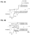
- FIGS. 9A and 9B the n-type cladding layer 12, the emission layer 13, and the electron reflection layer (eR) 14, or a quantum-wave interference layer, are shown.
- FIG. 9A shows an energy level of conduction and valence bands on the condition that no external voltage is applied to the LED 100
- FIG. 9B shows the energy level on the condition that the external voltage is applied thereto.
- the electron reflection layer (eR) 14, or a quantum-wave interference layer has a multiple quantum layer structure with 20 periods of a p-GaAs well layer as a first layer W and a p-Al 0.5 Ga 0.5 As barrier layer as a second layer B.
- Thicknesses of the first layer W and the second layer B are respectively determined according to Eqs. 1-1 and 1-2. Accordingly, electrons injected from the n-type cladding layer 12 into the emission layer 13 are reflected effectively by the electron reflection layer (eR) 14 and confined into the emission layer 13. Although the valence band of the electron reflection layer (eR) 14 also has a multiple period of energy level, holes are designed not to be reflected thereby. The respective thickness of the first layer W and the second layer B in the electron reflection layer (eR) 14 is designed to reflect electrons only. Therefore, holes injected from the p-type cladding layer 15 pass through the electron reflection layer (eR) 14 thus reaching the emission layer 13 easily and being confined therein by the n-type cladding layer 12.
- Luminous intensity was measured by varying the respective thickness of the first layer W and the second layer B.
- FIG. 10 shows a result when the thickness of the second layer B was fixed at 7nm and that of the first layer W was varied. As shown in FIG. 10, a peak of luminous intensity was obtained when the thickness of the first layer W was 5nm. Then, luminous intensity was measured fixing the thickness of the first layer W at 5nm and varying that of the second layer B, the result being shown in FIG. 11. When the second layer B has a thickness of 11nm, luminous intensity showed its peak.
- the LED 100 with the electron reflection layer (eR) 14 was found to have a maximum luminous intensity when the first layer W had a thickness of 5nm and the second layer B had a thickness of 11nm.
- the maximum luminous intensity was eightfold of that of a LED without the electron reflection layer (eR) 14.
- the quantum-wave interference layer comprising a p-GaAs layer and a p-Al 0.5 Ga 0.5 As layer can be an optimum electron reflection layer when the p-GaAs layer and the p-Al 0.5 Ga 0.5 As layer have thicknesses of 5nm and 11nm, respectively. So a quantum-wave interference layer comprising 10nm in thickness of a p-GaAs layer and 22nm in thickness of an n-Al 0.5 Ga 0.5 As layer may function as an electron transmission layer.
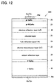
- FIG. 12 shows a light-emitting diode (LED) 200 having this electron transmission layer and the electron reflection layer as described in Example 1.
- LED light-emitting diode
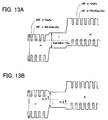
- the light-emitting device 200 also has a hole reflection layer (hR), whose energy diagrams are shown in FIGS. 13A and 13B.
- hR hole reflection layer
- thicknesses of a first layer hW and a second layer hB of the hole reflection layer (hR) were fixed at 1.0nm and 1.2nm, respectively.
- the light-emitting device 200 has a substrate 20 made of gallium arsenide (GaAs).
- the n-GaAs layer has a thickness of 55nm and an electron concentration of 2 x 10 18 /cm 3
- the n- Al 0.5 Ga 0.5 As layer has a thickness of 63nm and an electron concentration of 2 x 10 18 /cm 3 .
- An electron transmission layer (eT) 23 which has a thickness of about 0.6 ⁇ m and has a multiple layer structure comprising 20 pairs of an n-GaAs layer and an n-Al 0.5 Ga 0.5 As layer, is formed on the optical reflection layer 22.
- the n-GaAs layer has a thickness of 10nm and an electron concentration of 1 x 10 18 /cm 3
- the n- Al 0.5 Ga 0.5 As layer has a thickness of 22nm and an electron concentration of 1 x 10 18 /cm 3 .
- a hole reflection layer (hR) 24 which has a thickness of about 20nm and has a multiple layer structure comprising 10 pairs of an n-GaAs layer and an n-Al 0.5 Ga 0.5 As layer, is formed on the electron transmission layer (eT) 23.
- the n-GaAs layer has a thickness of 1nm and an electron concentration of 1 x 10 18 /cm 3
- the n-Al 0.5 Ga 0.5 As layer has a thickness of 1.2nm and an electron concentration of 1 x 10 18 /cm 3 .
- An emission 25 having a multiple layer structure is formed on the hole reflection layer (hR) 24.
- the following layers are laminated in the emission layer 25 on the hole reflection layer (hR) 24 in sequence: a non-doped i-Al 0.5 Ga 0.5 As layer having a thickness of 50nm; a non-doped i-Ga 0.89 In 0.11 As layer having a thickness of 14.5nm; a non-doped i-Al 0.5 Ga 0.5 As layer having a thickness of 3nm; a non-doped i-Ga 0.89 In 0.11 As layer having a thickness of 14.5mn; a non-doped i-Al 0.5 Ga 0.5 As layer having a thickness of 3nm; a non-doped i-Ga 0.89 In 0.11 As layer having a thickness of 14.5nm; and a non-doped i-Al 0.5 Ga 0.5 As layer having a thickness of 50nm.
- the i-Ga 0.89 In 0.11 As layer is a well layer and the i-Al 0.5 Ga 0.5 As layer is a barrier layer. Accordingly, the emission layer 25 has a multiple quantum well (MQW) structure, and has a thickness of about 0.15 ⁇ m.
- MQW multiple quantum well
- An electron reflection layer (eR) 26 which has a thickness of about 0.3 ⁇ m and has a multiple layer structure comprising 20 pairs of a p-GaAs layer and a p-Al 0.5 Ga 0.5 As layer, is formed on the emission layer 25.
- the p-GaAs layer has a thickness of 5nm and a hole concentration of 1 x 10 18 /cm 3
- the p-Al 0.5 Ga 0.5 As layer has a thickness of 11nm and a hole concentration of 1 x 10 18 /cm 3 .
- the substrate 20 has a diameter of 2.0 inches and the normal direction of its main surface is offset toward the [011] axis by 15 degree from the (100) plane.
- the light-emitting diode 200 was manufactured by gas source molecular beam epitaxial deposition (GS-MBE), the same method that the light-emitting diode 100 was manufactured by.
- the light-emitting diode 200 can be manufactured by metal organic chemical vapor deposition (MOCVD).
- FIG. 14 shows characteristics of the light-emitting diode. Its luminous wavelength is 908nm and half-width is 12nm. A temperature dependency of luminous wavelength and half-width of the light-emitting diode 200 in a range from 20°C to 80°C was measured. The temperature dependency of luminous wavelength is from 0.06nm/°C to 0.09nm/°C and a temperature dependency of half-width is less than 0.03nm/°C. The temperature dependencies of luminous wavelength and half-width in the light-emitting diode 200 are considerably improved compared with those in a general commercial product, whose temperature dependencies of luminous wavelength and half-width are 0.2nm/°C and 0.15nm/°C, respectively.
- a photocoupler formed by coupling the light-emitting diode 200 and a photodiode has a frequency response characteristics of 100 to 200MHz, which is much more larger than a frequency response characteristics of a commercial product, 20MHz.
- a quantum-wave interference layer for electrons is formed as a reflection layer 14.
- the electron reflection layer is not necessarily needed when the light-emitting diode 100 has a hole reflection layer.
- a light-emitting diode which has a hole reflection layer (hR) formed on the n-type (or the negative electrode) side of the emission layer 13 and a p-cladding layer 15 formed on the p-type (or the positive electrode side) of the emission layer 13, does not necessarily have a quantum-wave interference layer for electrons.
- hR hole reflection layer
- a quantum-wave interference layer for holes improves effectivity of the diode.
- two kinds of quantum-wave interference layers are formed for electrons in the light-emitting diode 200.
- the two kinds of quantum-wave interference layers function as the electron transmission layer 23 and the electron reflection layer 26, and the emission layer 25 and the hole reflection layer 24 are formed between the two kinds of quantum-wave interference layers for electrons.
- the hole reflection layer 24 is not necessarily needed.
- a diode can be formed to have the emission layer 25, the electron transmission layer 23 formed on the n-type (or the negative electrode) side of the emission layer 25, and the electron reflection layer 26 formed on the p-type (or the positive electrode) side of the emission layer 25 and a quantum-wave interference layer for holes is not existed.
- a pair of quantum-wave interference layers as an electron transmission layer and an electron reflection layer, respectively, improves effectivity of a light-emitting diode as in the present invention.
- the light-emitting diode of the present invention comprises an emission layer, a hole reflection layer formed on the negative electrode side of the emission layer and a hole transmission layer formed on the positive side of the emission layer.
- the light-emitting diode can comprise both quantum-wave interference layers for holes, or a hole transmission layer and a hole reflection layer, and either one of an electron transmission layer and an electron reflection layer. Order of disposition between the electron transmission layer and the hole reflection layer or between the electron reflection layer and the hole transmission layer is arbitrary.
- diodes without ⁇ layers are shown. Because ⁇ layers can vary band gap energy at a potential interface sharply, interference effect of quantum-wave can be more improved by forming ⁇ layers.
- the layer having a multiple period structure can be made of binary, ternary and quaternary compounds such as Al x Ga y In 1-x-y P or Al x Ga y In 1-x-y As, selecting arbitrary composition ratio within the range of 0 ⁇ x ⁇ 1, 0 ⁇ y ⁇ 1, and 0 ⁇ x+y ⁇ 1 .
- a light-emitting diode was used to show the effectivity of this invention.
- a quantum-wave interference layer which comprises multiple periods of a pair of an Al x Ga 1-x As first layer and an Al y Ga 1-y As second layer whose band width is larger than that of the first layer (0 ⁇ x ⁇ y ⁇ 1), as a reflection layer or a transmission layer of electrons or holes is not necessarily limited to a light-emitting diode, and can be applied to an arbitrary semiconductor device such as a photodiode, a light-receiving device (e.g., a solar battery), a bipolar or a field-effect transistor, a variable capacity device, and an arbitrary semiconductor device.
- a quantum-wave interference layer which comprises an Al x Ga 1-x As first layer and an Al y Ga 1-y As second layer whose band width is larger than that of the first layer (0 ⁇ x ⁇ y ⁇ 1), can be formed in a photovoltaic device having a pn junction structure.
- an electron reflection layer which reflects electrons is formed in a p-layer
- a hole reflection layer which reflects holes is formed in an n-layer.
- a light-receiving device having a pin type, pp - n type or pn - n type and pn type, it is effective to form a quantum-wave interference layer in at least one of an n-layer, a p - -layer, an n - -layer and a p-layer. Effectivity of such a light-receiving device can be also improved when plural quantum-wave interference layers comprising multiple periods of a pair of a first layer made of Al x Ga 1-x As and a second layer made of Al y Ga 1-y As, whose band width is larger than that of the first layer, are formed through a middle layer which has the same band width as that of the first layer or the second layer.
- a quantum-wave interference layer comprising multiple periods of a pair of a first layer made of Al x Ga 1-x As and a second layer made of Al y Ga 1-y As, whose band width is larger than that of the first layer, can be formed in a base region of a bipolar transistor and a channel region of a field effect transistor.
- doping arbitrary impurities, or adding dopants into the first layer made of Al x Ga 1-x As and a second layer made of Al y Ga 1-y As can be applied.
- a part of the composition elements, or aluminum (Al), gallium (Ga) and arsenide (As) can be replaced with other elements in the same group.
- group III composition elements such as Al and Ga can be replaced with other group III elements, e.g., B, In and Tl.
- group V composition elements such as As can be replaced with other group V elements, e.g., N, P, Sb and Bi.
- the electron reflection layer (eR) 14 has a multiple quantum layer structure with 20 periods of a p-GaAs well layer as a first layer W and a p-Al 0.5 Ga 0.5 As barrier layer as a second layer B. Each thickness of the first and the second layers is determined by one fourth of a quantum-wave wavelength of electrons in each of the first and the second layers. As a result, luminous intensity of the light-emitting diode is improved.
Landscapes
- Led Devices (AREA)
- Light Receiving Elements (AREA)
- Semiconductor Lasers (AREA)
Applications Claiming Priority (2)
| Application Number | Priority Date | Filing Date | Title |
|---|---|---|---|
| JP24165299 | 1999-08-27 | ||
| JP24165299A JP2001068793A (ja) | 1999-08-27 | 1999-08-27 | 量子波干渉層を有した半導体素子 |
Publications (1)
| Publication Number | Publication Date |
|---|---|
| EP1085583A2 true EP1085583A2 (de) | 2001-03-21 |
Family
ID=17077513
Family Applications (1)
| Application Number | Title | Priority Date | Filing Date |
|---|---|---|---|
| EP00118585A Withdrawn EP1085583A2 (de) | 1999-08-27 | 2000-08-25 | Halbleiteranordnungen mit Quantenwelleninterferenzschichten |
Country Status (2)
| Country | Link |
|---|---|
| EP (1) | EP1085583A2 (de) |
| JP (1) | JP2001068793A (de) |
Families Citing this family (1)
| Publication number | Priority date | Publication date | Assignee | Title |
|---|---|---|---|---|
| DE102011116367A1 (de) * | 2011-10-19 | 2013-04-25 | Bluepoint Medical Gmbh & Co. Kg | Vorrichtung zur hoch aufgelösten Bestimmung der Konzentration von Substanzen in fluiden Medien |
-
1999
- 1999-08-27 JP JP24165299A patent/JP2001068793A/ja active Pending
-
2000
- 2000-08-25 EP EP00118585A patent/EP1085583A2/de not_active Withdrawn
Also Published As
| Publication number | Publication date |
|---|---|
| JP2001068793A (ja) | 2001-03-16 |
Similar Documents
| Publication | Publication Date | Title |
|---|---|---|
| US6175123B1 (en) | Semiconductor devices with quantum-wave interference layers | |
| EP0731510B1 (de) | Halbleitervorrichtung mit einem Miniband | |
| US6664561B2 (en) | Light-receiving device with quantum-wave interference layers | |
| EP1085583A2 (de) | Halbleiteranordnungen mit Quantenwelleninterferenzschichten | |
| KR20000070646A (ko) | 광전자 반도체 소자 | |
| EP1085581A2 (de) | Halbleiteranordnung mit Quantenwelleninterferenzschichten | |
| US6420727B1 (en) | Light-emitting semiconductor device with quantum-wave interference layers | |
| EP1085582A2 (de) | Lichtemittierende Halbleiteranordnung mit Quantenwelleninterferenzschichten | |
| US6188082B1 (en) | Diodes with quantum-wave interference layers | |
| US6818916B2 (en) | Light-receiving device with quantum-wave interference layers | |
| US6552412B2 (en) | Semiconductor device with quantum-wave interference layers | |
| US6479842B1 (en) | Field effect transistor with a quantum-wave interference layer | |
| US6486490B1 (en) | Light-emitting device with a quantum-wave interference layer | |
| EP0996166A2 (de) | Halbleiteranordnungen mit einer Mehrfach-Quantenbarrierestruktur | |
| EP0935294A1 (de) | Bauelement mit variabler Kapazität und mit Quantenwellen-Interferenz-Schichten | |
| EP0967658A2 (de) | Halbleiteranordnung mit Quanten-Wellen-Interferenz-Schichten | |
| US6337508B1 (en) | Transistor with a quantum-wave interference layer | |
| JP3544160B2 (ja) | 量子波干渉層を有した受光素子 | |
| EP1011147A2 (de) | Transistoren mit einer Quantenwelleninterferenzschicht | |
| EP0996169A2 (de) | Halbleiteranordnung mit einer Begrenzungsschicht | |
| JP2000114601A (ja) | 量子波干渉層を有した半導体素子及び半導体素子を構成する量子波干渉層の設計方法 |
Legal Events
| Date | Code | Title | Description |
|---|---|---|---|
| PUAI | Public reference made under article 153(3) epc to a published international application that has entered the european phase |
Free format text: ORIGINAL CODE: 0009012 |
|
| AK | Designated contracting states |
Kind code of ref document: A2 Designated state(s): AT BE CH CY DE DK ES FI FR GB GR IE IT LI LU MC NL PT SE |
|
| AX | Request for extension of the european patent |
Free format text: AL;LT;LV;MK;RO;SI |
|
| STAA | Information on the status of an ep patent application or granted ep patent |
Free format text: STATUS: THE APPLICATION IS DEEMED TO BE WITHDRAWN |
|
| 18D | Application deemed to be withdrawn |
Effective date: 20040302 |