EP1087460A2 - Dispositif pour la répartition et la synthèse de puissance et équipement mobile de communication l'utilisant - Google Patents
Dispositif pour la répartition et la synthèse de puissance et équipement mobile de communication l'utilisant Download PDFInfo
- Publication number
- EP1087460A2 EP1087460A2 EP00119943A EP00119943A EP1087460A2 EP 1087460 A2 EP1087460 A2 EP 1087460A2 EP 00119943 A EP00119943 A EP 00119943A EP 00119943 A EP00119943 A EP 00119943A EP 1087460 A2 EP1087460 A2 EP 1087460A2
- Authority
- EP
- European Patent Office
- Prior art keywords
- power distributing
- synthesizing device
- terminal
- laminated body
- transmission lines
- Prior art date
- Legal status (The legal status is an assumption and is not a legal conclusion. Google has not performed a legal analysis and makes no representation as to the accuracy of the status listed.)
- Withdrawn
Links
Images



Classifications
-
- H—ELECTRICITY
- H01—ELECTRIC ELEMENTS
- H01P—WAVEGUIDES; RESONATORS, LINES, OR OTHER DEVICES OF THE WAVEGUIDE TYPE
- H01P5/00—Coupling devices of the waveguide type
- H01P5/12—Coupling devices having more than two ports
- H01P5/16—Conjugate devices, i.e. devices having at least one port decoupled from one other port
Definitions
- the present invention relates to a power distributing and synthesizing device, and more particularly to a power distributing and synthesizing device for distributing or synthesizing a high-frequency power used for communication equipment utilizing the microwave band.
- Fig. 8 is an equivalent circuit diagram of a conventional Wilkinson type power distributing and synthesizing device.
- the power distributing and synthesizing device 50 comprises first and second transmission lines 51 and 52, first to three signal terminals 531 - 533, a resistor 54, and capacitors 551 - 553.
- the connection portion between one end of the first transmission line 51 and one end of the second transmission line 52 is used as a first signal terminal (synthesis terminal) 531
- the other terminal of the first transmission line 51 is used as a second signal terminal (distribution terminal) 532
- the other terminal of the second transmission line 52 is used as a third signal terminal (distribution terminal) 533.
- the second signal terminal 532 and the third signal terminal 533 are connected via the resistor 54.
- the first to third signal terminals 531 - 533 are connected to a ground via the capacitors 551 - 553.
- the power distributing and synthesizing device 50 When the power distributing and synthesizing device 50 is used as a distributor, a high-frequency power is inputted from the first signal terminal 531, and the inputted high-frequency power is outputted from the second and third signal terminals 532 and 533. On the other hand, when the power distributing and synthesizing device 50 is used as a synthesizer, a high-frequency power is inputted from the second and third signal terminals 532 and 533, and the inputted high-frequency power is outputted from the first signal terminal 531.
- the impedance of the circuit to be connected to the first signal terminal 531 be Z1
- the impedance of the circuits to be connected to the second and third signals 532 and 533 be Z23.
- the present invention provides in its first aspect a power distributing and synthesizing device comprising first and second transmission lines; a synthesis terminal constituted of the connection portion between one end of the first transmission line and one end of the second transmission line; a first distribution terminal constituted of the other end of the first transmission line; a second distribution terminal constituted of the other end of the second transmission line; a resistor connected between the first distribution terminal and the second distribution terminal; and at least one LC serial resonator compising an inductor and a capacitor.
- this power distributing and synthesizing device at least one terminal among the synthesis terminal, the first distribution terminal, and the second distribution terminal is connected to the ground via the at least one LC resonator.
- the present invention provides in its first aspect a power distributing and synthesizing device further comprising a laminated body formed by laminating a plurality of dielectric layers; strip line electrodes provided within the laminated body; and via hole electrodes provided within the laminated body.
- each of the first and second transmission lines is formed of the strip line electrodes;
- the inductor is formed of at least one of the strip line electrode and the via hole electrode;
- the capacitor is formed of a plurality of electrodes formed within the laminated body so as to be opposed to each other across the dielectric layers.
- the present invention provides in its second aspect a power distributing and synthesizing device comprising first and second transmission lines; a synthesis terminal constituted of the connection portion between one end of the first transmission line and one end of the second transmission line; a first distribution terminal constituted of the other end of the first transmission line; a second distribution terminal constituted of the other end of the second transmission line; a resistor connected between the first distribution terminal and the second distribution terminal; and at least one LC serial resonator comprising an inductor and a capacitor.
- a capacitor is connected in parallel with at least one of the first and second transmission lines.
- the present invention provides in its second aspect a power distributing and synthesizing device further comprising a laminated body formed by laminating a plurality of dielectric layers; and strip line electrodes provided within the laminated body.
- a power distributing and synthesizing device further comprising a laminated body formed by laminating a plurality of dielectric layers; and strip line electrodes provided within the laminated body.
- each of the first and second transmission lines is formed of the strip line electrodes; and the capacitor is formed of a plurality of electrodes formed within the laminated body so as to be opposed to each other across the dielectric layers.
- each of the strip line electrodes forming said first and second transmission lines have a helical coil shape.
- the mobile communication equipment in accordance with the present invention uses the above-described power distributing and synthesizing device.
- an LC serial resonator is connected between at least one terminal among the synthesis terminal, the first distribution terminal, and the second distribution terminal and the ground, it is possible to generate the attenuation pole by a serial resonance of the LC serial resonator, in the vicinity of the resonance frequency of an inputted power (signal). This allows high-frequency signals in the vicinity of the resonance frequency to be removed.
- the power distributing and synthesizing device in accordance with the second aspect of the present invention since a capacitor is connected in parallel with at least one of the first and second transmission lines, it is possible to generate the attenuation pole by a parallel resonance of the LC parallel resonator comprising at least one of the first and second transmission lines and a capacitor, in the vicinity of the resonance frequency of an inputted power (signal). This allows high-frequency signals in the vicinity of the resonance frequency to be removed.
- the power distributing and synthesizing device which is capable of sufficiently securing the isolation between the synthesis terminal and the distribution terminals, and which allows a cost reduction and reduction in size, it is possible to achieve a small-sized transmitter which is superior in characteristics.
- Fig. 1 is an equivalent circuit diagram of a power distributing and synthesizing device in accordance with a first embodiment.
- the power distributing and synthesizing device 10 comprises first to third signal terminals P1 - P3, first and second transmission lines 11 and 12, a resistor 13, and LC serial resonators 141 - 143.
- the LC serial resonators 141 - 143 comprise inductors L1 - L3 and capacitors C11 - C13, respectively.
- first transmission line 11 and one end of the second transmission line 12 are connected, and the connection portion thereof is used as a first signal terminal (synthesis terminal) P1.
- the other end of the first transmission line 11 is used as a second signal terminal (distribution terminal) P2, and the other end of the second transmission line 12 is used as a third signal terminal (distribution terminal) P3.
- a resistor (isolation resistor) 13 is connected between the second signal terminal P2 and the third signal terminal P3.
- LC serial resonators 141 - 143 are connected between the respective first to third signal terminals P1 - P3 and the ground.
- Fig. 2 is an explosive perspective view of a power distributing and synthesizing device having the equivalent circuit shown in Fig. 1.
- the power distributing and synthesizing device 10 has a laminated body 15, and a resistor 13 is mounted on the top surface of the laminated body 15.
- External terminals T11 - T15 are each provided from the top surface to the bottom surface of the laminated body 15.
- the external terminals T11, T13, and T14 constitute the first to third signal terminals P1 - P3 (Fig. 1) of the power distributing and synthesizing device 10, respectively, and the external terminals T12 and T15 constitute ground terminals.
- the laminated body 15 is formed by, for example, sequentially laminating first to sixth dielectric layers 151 - 156 constituted of a low-temperature fired ceramic of which main constituents are barium oxide, aluminum oxide, and silica, and which can be fired at 850°C to 1000°C, and then firing the laminated dielectric layers.
- a land La for mounting the resistor 13 is formed on the top surface of the first dielectric layer 151.
- Strip line electrodes SL11 and SL21, and strip line electrodes SL21 and SL22 each of which has a helical coil shape are formed on the top surfaces of the second and third dielectric layers 152 and 153, respectively.
- Ground electrodes Gp1 and Gp2 are formed on the top surfaces of the fourth and sixth dielectric layers 154 and 156, respectively.
- Capacitor electrodes Cp1 - Cp3 are formed on the top surface of the fifth dielectric layer 155.
- a via hole electrode Vh1 is formed in each of the third and fourth dielectric layers 153 and 154 so as to pass through the dielectric layers 153 and 154, and via hole electrodes Vh2 and Vh3 are each formed in the first to fourth dielectric layers 151 - 154 so as to pass through the dielectric layers 151 - 154. Also, a via hole electrode Vh is formed in the second dielectric layer 152 so as to pass through the dielectric layers 152.
- the strip line electrodes SL11, SL12 and the via hole electrode Vh form the first transmission line 11 (Fig. 1), and the strip line electrodes SL21, SL22 and the via hole electrode Vh form the second transmission line 12 (Fig. 1).
- the via hole electrode Vh1 passing through the third and fourth dielectric layers 153 and 154 forms the inductor L1 of the LC serial resonator 141, and the via hole electrodes Vh2 and Vh3 passing through the first to fourth dielectric layers 151 and 154 form the inductors L2 and L3 of the LC serial resonators 142 and 143, respectively.
- the capacitor electrodes Cp1 - Cp3 and the ground electrodes Gp1 and Gp2 which are opposed to each other across the fourth dielectric layers 154 and across the fifth dielectric layer 155, form the capacitors C11 - C13 of the LC serial resonators 141 - 143.
- the ground electrodes Gp1 and Gp2 constitute another capacitor electrode.
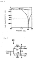
- Fig. 3 illustrates the pass characteristics of the power distributing and synthesizing device shown in Fig. 2.
- the solid line represents the pass characteristics of the power distributing and synthesizing device 10 in accordance with the present embodiment (Fig. 1), and the broken line represents those of the conventional power distributing and synthesizing device 50 (Fig. 8).
- the attenuation pole by the serial resonance of the LC serial resonators 141 - 143 occurs in the vicinity of the resonance frequency, 2.15 GHz and that the attenuation value at the resonance frequency is about 56.9 dB.
- This attenuation value is about 4.5 times larger than that of the conventional power distributing and synthesizing device 50 (broken line) of which attenuation value is about 12.7 dB.
- the LC serial resonators are connected between the first to three signal terminals and the ground, the attenuation pole by the serial resonance of the LC serial resonators can be generated in the vicinity of the resonance frequency. This allows high-frequency signals in the vicinity of the resonance frequency to be removed, and thereby allows the isolation between the first and second signal terminals, or between the first and third signal terminals to be sufficiently secured.
- the position of the attenuation pole formed by the serial resonance of the LC serial resonators can be easily changed. This permits high-frequency signals having an intended frequency to be removed in the power distributing and synthesizing device, and thereby permits the isolation between the synthesis terminal and distribution terminals to be sufficiently secured.
- the first embodiment of the present invention has a laminated body formed by laminating the first to sixth dielectric layers, forms each of the first and second transmission lines of strip line electrodes provided within the laminated body, forms the inductor constituting each of the LC serial resonators of a via hole electrode provided within the laminated body, and forms the LC serial resonator of a plurality of the electrodes provided within the laminated body so as to be opposed to each other across the dielectric layers. Therefore, the number of components of the power distributing and synthesizing device can be reduced. This results in an cost-reduction and a reduction in size of the power distributing and synthesizing device.
- the mounting surface thereof can be decreased.
- each of the strip line electrodes forming the first and second transmission lines has a helical coil shape, the flux generated by the current flowing through the first and second transmission lines is large, and hence the self inductances of the first and second transmission lines are large.
- the overall length of the first and second transmission lines can be shorter than ⁇ /4, the loss of the power distributing and synthesizing device can be decreased and the size of the power distributing and synthesizing device can be further reduced.
- Fig. 4 is an equivalent circuit diagram of a power distributing and synthesizing device in accordance with a second embodiment.
- the power distributing and synthesizing device 20 comprises first to third signal terminals P1 - P3, first and second transmission lines 11 and 12, resistor 13, and capacitors C21 - C25.
- first transmission line 11 and one end of the second transmission line 12 are connected, and the connection portion thereof is used as a first signal terminal (synthesis terminal) P1.
- the other end of the first transmission line 11 is used as a second signal terminal (distribution terminal) P2, and the other end of the second transmission line 12 is used as a third signal terminal (distribution terminal) P3.
- a resistor (isolation resistor) 13 is connected between the second signal terminal P2 and the third signal terminal P3. Also, a capacitor 21 is connected in parallel with the first transmission line 11, and a capacitor 22 is connected in parallel with the second transmission line 12, and a capacitor 23 - 25 are connected between the respective first to third signal terminals P1 - P3 and the ground.
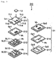
- Fig. 5 is an explosive perspective view of a power distributing and synthesizing device having the equivalent circuit shown in Fig. 4.
- the power distributing and synthesizing device 20 has a laminated body 21, and a resistor 13 is mounted on the top surface of the laminated body 21.
- External terminals T11 - T15 are each provided from the top surface to the bottom surface of the laminated body 21.
- the external terminals T11, T13 and T14 constitute the first to third signal terminals P1 - P3 (Fig. 4) of the power distributing and synthesizing device 20, respectively, and the external terminals T12 and T15 constitute ground terminals.
- the laminated body 21 is formed by, for example, sequentially laminating first to seventh dielectric layers 211 - 217 constituted of a low-temperature fired ceramic of which main constituents are barium oxide, aluminum oxide, and silica, and which can be fired at 850°C to 1000°C.
- a land La for mounting the resistor 13 is formed on the top surface of the first dielectric layer 211.
- Ground electrodes Gp1 and Gp2 are formed on the top surfaces of the second and fifth dielectric layers 212 and 215, respectively.
- Strip line electrodes SL11 and SL21, and strip line electrodes SL12 and SL22 each of which has a helical coil shape are formed on the top surfaces of the third and fourth dielectric layers 213 and 214, respectively.
- Capacitor electrodes Cp1 - Cp3 are formed on the top surface of the sixth and seventh dielectric layer 216 and 217.
- a via hole electrode Vh is formed in each of the first to sixth dielectric layers 211 - 216 so as to pass through the dielectric layers 211 and 216.
- the strip line electrodes SL11, SL12 and the via hole electrode Vh form the first transmission line 11 (Fig. 4), and the strip line electrodes SL21, SL22 and the via hole electrode Vh form the second transmission line 12 (Fig. 4). Also, the capacitor electrodes Cp1 and Cp2 opposed to each other across the sixth dielectric layer 216, and the capacitor electrodes Cp1 and Cp3 opposed to each other across the sixth dielectric layer 216, form the capacitors C21 and C22, respectively.
- the strip line electrodes SL21, SL22 and the ground electrode Gp2 form the capacitor C23
- the strip line electrode SL11 and the ground electrode Gp1 form the capacitor C24
- the strip line electrode SL21 and the ground electrode Gp1 form the capacitor C25.
- Fig. 6 illustrates the pass characteristics of the power distributing and synthesizing device shown in Fig. 4.
- the solid line represents the pass characteristics of the power distributing and synthesizing device 20 (Fig. 4), and the broken line represents those of the conventional power distributing and synthesizing device 50 (Fig. 8).
- the attenuation pole by the parallel resonance of the LC parallel resonators comprising the first and second transmission lines and capacitors occurs in the vicinity of the resonance frequency, 2.15 GHz and that the attenuation value at the resonance frequency is about 56.1 dB.
- This attenuation value is about 4.4 times larger than that of the conventional power distributing and synthesizing device 50 (broken line) of which attenuation value is about 12.7 dB.
- the attenuation pole by the parallel resonance of the LC parallel resonators comprising the first and second transmission lines and capacitors can be generated in the vicinity of the resonance frequency. This allows high-frequency signals in the vicinity of the resonance frequency to be removed, and thereby allows the isolation between the first and second signal terminals, or between the first and third signal terminals to be sufficiently secured.
- the position of the attenuation pole formed by the parallel resonance of the LC parallel resonators comprising the first and second transmission lines and capacitors can be easily changed. This permits high-frequency signals having an intended frequency to be removed in the power distributing and synthesizing device, and thereby permits the isolation between the synthesis terminal and distribution terminals to be sufficiently secured.
- the second embodiment of the present invention has a laminated body formed by laminating the first to seventh dielectric layers, forms each of the first and second transmission lines of strip line electrodes provided within the laminated body, and forms each of the capacitors to be connected in parallel with the first and second transmission lines of a plurality of the electrodes provided within the laminated body so as to be opposed to each other across the dielectric layer. Therefore, the number of components of the power distributing and synthesizing device can be reduced. This results in an cost-reduction and a reduction in size of the power distributing and synthesizing device.
- each of the strip line electrodes forming the first and second transmission lines has a helical coil shape, the flux generated by the current flowing through the first and second transmission lines is large, and hence the self inductances of the first and second transmission lines are large.
- the overall length of the first and second transmission lines can be shorter than ⁇ /4, the loss of the power distributing and synthesizing device can be decreased and the size of the power distributing and synthesizing device can be further reduced.
- FIG. 7 is a block diagram showing typical mobile communication equipment.
- a transmitter 30 which is one of mobile communication equipment comprises a modulation circuit 31, 180° hybrid circuits 32 and 33, mixers 34 and 35, a local oscillator 36, in-phase distributor 37, and an antenna 38.
- a baseband signal including a information signal to be transmitted is inputted to the modulation circuit 31, and the modulation circuit 31 outputs the modulation signal modulated by a predetermined modulation method such as the amplitude modulation or the frequency modulation to the 180° hybrid circuits 32.
- the 180° hybrid circuits 32 distributes the inputted signal to two signals having phases opposite to each other, and outputs one signal to the mixer 34, and outputs the other signal to the mixer 35.
- the local oscillator 36 generates a predetermined local oscillation signal, and outputs it to the in-phase distributor 37.
- the in-phase distributor 37 in-phase distributes the inputted local oscillation signal to the two signals, and outputs it to the mixer 34 and 35.
- the mixer 34 mixes the two inputted signals, and output them to the 180° input terminal of the 180° hybrid circuit 33.
- the mixer 35 mixes the two inputted signals, and outputs them to the 0° input terminal of the 180° hybrid circuit 33.
- the 180° hybrid circuit 33 power-synthesizes the two inputted signals in phases opposite to each other, and outputs the synthesized signal to the antenna 38 to emit.
- the power distributing and synthesizing devices 10 and 20 shown in Figs. 1 and 4, respectively, are used.
- this transmitter which is one of the above-describe mobile communication equipment, since the power distributing and synthesizing device capable of sufficiently securing the isolation between the synthesis terminal and the distribution terminals, and allowing a cost reduction and a reduction in size is used, a small sized transmitter which is superior in characteristics can be achieved.
- each of dielectric layers is constituted of a ceramic of which main constituents are barium oxide, aluminum oxide, and silica.
- any material having a dielectric constant ( ⁇ r) not less than 1 can be used.
- a ceramic of which main constituents are magnesium oxide and silica, or a fluorine base resin also provides a similar effect.
- inductors or capacitors are provided within the laminated layer.
- the present invention may be constructed of chip inductors or chip capacitors.
- the power distributing and synthesizing device is used as an in-phase distributor of the transmitter which is one of the mobile communication equipment.
- the power distributing and synthesizing device may, however, be used as an in-phase distributor of a receiver. In this case also, a similar effect can be provided.
- the LC serial resonators are connected between the first to three signal terminals and the ground, the attenuation pole by the serial resonance of the LC serial resonators can be generated in the vicinity of the resonance frequency. This allows high-frequency signals in the vicinity of the resonance frequency to be removed, and thereby allows the isolation between the synthesis terminal and distribution terminals to be sufficiently secured.
- the position of the attenuation pole formed by the serial resonance of the LC serial resonators can be easily changed. This allows high-frequency signals having an intended frequency to be removed in the power distributing and synthesizing device, and thereby allows the isolation between the synthesis terminal and distribution terminals to be sufficiently secured.
- the power distributing and synthesizing device in accordance with the first aspect of the present invention has a laminated body formed by laminating a plurality of the dielectric layers, forms each of the first and second transmission lines of strip line electrodes provided within the laminated body, forms the inductor constituting each of the LC serial resonators of one of strip line electrode and via hole electrode provided within the laminated body, and forms the capacitor constituting each of the LC serial resonators of a plurality of the electrodes provided within the laminated body so as to be opposed to each other across the dielectric layers. Therefore, the number of components of the power distributing and synthesizing device can be reduced. This results in an cost-reduction and a reduction in size of the power distributing and synthesizing device.
- the attenuation pole by the parallel resonance of the LC parallel resonators comprising the first and second transmission lines and capacitors can be generated in the vicinity of the resonance frequency. This allows high-frequency signals in the vicinity of the resonance frequency to be removed.
- the position of the attenuation pole formed by the parallel resonance of the LC parallel resonators comprising the first and second transmission lines and capacitors can be easily changed. This allows high-frequency signals having an intended frequency to be removed in the power distributing and synthesizing device, and thereby allows the isolation between the synthesis terminal and distribution terminals to be sufficiently secured.
- the power distributing and synthesizing device in accordance with the second aspect of the present invention has a laminated body formed by laminating a plurality of the dielectric layers, forms each of the first and second transmission lines of strip line electrodes provided within the laminated body, and forms each of the capacitors connected in parallel with the first and second transmission lines of a plurality of the electrodes provided within the laminated body so as to be opposed to each other across the dielectric layer. Therefore, the number of components of the power distributing and synthesizing device can be reduced. This results in an cost-reduction and a reduction in size of the power distributing and synthesizing device.
- each of the strip line electrodes forming the first and second transmission lines has a helical coil shape, the flux generated by the current flowing through the first and second transmission lines is large, and hence the self inductances of the first and second transmission lines are large.
- the overall length of the first and second transmission lines can be shorter than ⁇ /4, the loss of the power distributing and synthesizing device can be decreased and the size of the power distributing and synthesizing device can be further reduced.
- the power distributing and synthesizing device which is capable of sufficiently securing the isolation between the synthesis terminal and the distribution terminals, and which allows a cost reduction and a reduction in size, a small sized transmitter which is superior in characteristics can be achieved.
Landscapes
- Control Of Motors That Do Not Use Commutators (AREA)
- Filters And Equalizers (AREA)
- Transmitters (AREA)
Applications Claiming Priority (2)
| Application Number | Priority Date | Filing Date | Title |
|---|---|---|---|
| JP27277299A JP3473518B2 (ja) | 1999-09-27 | 1999-09-27 | 電力分配合成器及びそれを用いた移動体通信機 |
| JP27277299 | 1999-09-27 |
Publications (2)
| Publication Number | Publication Date |
|---|---|
| EP1087460A2 true EP1087460A2 (fr) | 2001-03-28 |
| EP1087460A3 EP1087460A3 (fr) | 2002-09-11 |
Family
ID=17518538
Family Applications (1)
| Application Number | Title | Priority Date | Filing Date |
|---|---|---|---|
| EP00119943A Withdrawn EP1087460A3 (fr) | 1999-09-27 | 2000-09-13 | Dispositif pour la répartition et la synthèse de puissance et équipement mobile de communication l'utilisant |
Country Status (3)
| Country | Link |
|---|---|
| US (1) | US6748207B1 (fr) |
| EP (1) | EP1087460A3 (fr) |
| JP (1) | JP3473518B2 (fr) |
Cited By (2)
| Publication number | Priority date | Publication date | Assignee | Title |
|---|---|---|---|---|
| WO2007063344A1 (fr) * | 2005-11-30 | 2007-06-07 | Selex Sensors And Airborne Systems Limited | Diviseur / combinateur de puissance hyperfrequence |
| EP2127018A4 (fr) * | 2006-12-29 | 2011-11-02 | Emw Antenna Co Ltd | Diviseur de puissance et combinateur de puissance employant une ligne de transmission droite/gauche composite à double bande |
Families Citing this family (14)
| Publication number | Priority date | Publication date | Assignee | Title |
|---|---|---|---|---|
| KR100529581B1 (ko) * | 2002-12-09 | 2005-11-22 | 한국전자통신연구원 | 초고주파 윌켄슨 전력분배기 |
| US7468640B2 (en) | 2004-02-06 | 2008-12-23 | Murata Manufacturing Co., Ltd. | Balanced splitter |
| JP2010251904A (ja) * | 2009-04-13 | 2010-11-04 | Mitsubishi Electric Corp | 電力分配合成器 |
| CN102255127A (zh) * | 2010-05-20 | 2011-11-23 | 上海明珠广播电视科技有限公司 | 一种用于调频大功率多路射频信号的合成器 |
| JP5618034B2 (ja) * | 2012-08-10 | 2014-11-05 | 株式会社村田製作所 | 分岐ケーブル |
| WO2015022839A1 (fr) * | 2013-08-12 | 2015-02-19 | 株式会社村田製作所 | Diviseur de puissance |
| CN107403989A (zh) * | 2016-05-20 | 2017-11-28 | 鸿富锦精密工业(深圳)有限公司 | 功率分配电路及应用所述功率分配电路的功率分配器 |
| TWI637553B (zh) * | 2016-05-20 | 2018-10-01 | 新加坡商雲網科技新加坡有限公司 | 功率分配電路及應用所述功率分配電路的功率分配器 |
| KR102299451B1 (ko) * | 2016-12-20 | 2021-09-08 | 한국전자기술연구원 | 광대역 특성을 갖는 분배/합성기 |
| CN108988816A (zh) * | 2018-10-15 | 2018-12-11 | 深圳飞骧科技有限公司 | 谐波抑制功率合成器及射频功率放大器 |
| JP7163972B2 (ja) * | 2018-12-12 | 2022-11-01 | 株式会社村田製作所 | 電力分配器 |
| WO2022080393A1 (fr) * | 2020-10-14 | 2022-04-21 | 株式会社村田製作所 | Circuit amplificateur de puissance et dispositif de communication |
| JP7581939B2 (ja) * | 2021-02-09 | 2024-11-13 | 住友電気工業株式会社 | ウィルキンソン分配器、ウィルキンソン合成器、及び増幅器 |
| WO2022196640A1 (fr) | 2021-03-17 | 2022-09-22 | Tdk株式会社 | Composant électronique et dispositif de communication |
Family Cites Families (13)
| Publication number | Priority date | Publication date | Assignee | Title |
|---|---|---|---|---|
| DE2453605B2 (de) * | 1974-11-12 | 1976-09-09 | Siemens AG, 1000 Berlin und 8000 München | Wellenleiter-koppler zur gleichmaessigen aufteilung oder zusammenschaltung von signalenergie |
| US4812849A (en) * | 1984-09-17 | 1989-03-14 | General Dynamics Corporation | Nonquadrature correction circuit |
| US5390337A (en) * | 1992-05-01 | 1995-02-14 | Scientific-Atlanta, Inc. | Combination surge and diplex filter for CATV distribution systems |
| JP3333014B2 (ja) * | 1993-10-04 | 2002-10-07 | ティーディーケイ株式会社 | 高周波信号分配・合成器 |
| US5430418A (en) | 1994-02-14 | 1995-07-04 | At&T Corp. | Power combiner/splitter |
| US5596325A (en) * | 1995-07-07 | 1997-01-21 | Nonlinear Technologies, Inc. | FM-CW radar transceiver |
| JP3646146B2 (ja) | 1995-07-31 | 2005-05-11 | 神田通信工業株式会社 | 無線電話機親機 |
| US6075991A (en) * | 1996-03-08 | 2000-06-13 | Watkins-Johnson Company | Wireless base station with near-far gain compensation |
| JPH09266430A (ja) | 1996-03-28 | 1997-10-07 | Sumitomo Kinzoku Electro Device:Kk | 積層フィルタ |
| US5821831A (en) * | 1996-05-10 | 1998-10-13 | Eagle Comtronics, Inc. | Diplex filter comprising monotonic poles |
| US5832376A (en) * | 1996-07-12 | 1998-11-03 | Endgate Corporation | Coplanar mixer assembly |
| US5929729A (en) * | 1997-10-24 | 1999-07-27 | Com Dev Limited | Printed lumped element stripline circuit ground-signal-ground structure |
| US5939939A (en) * | 1998-02-27 | 1999-08-17 | Motorola, Inc. | Power combiner with harmonic selectivity |
-
1999
- 1999-09-27 JP JP27277299A patent/JP3473518B2/ja not_active Expired - Lifetime
-
2000
- 2000-09-13 EP EP00119943A patent/EP1087460A3/fr not_active Withdrawn
- 2000-09-27 US US09/671,839 patent/US6748207B1/en not_active Expired - Lifetime
Cited By (4)
| Publication number | Priority date | Publication date | Assignee | Title |
|---|---|---|---|---|
| WO2007063344A1 (fr) * | 2005-11-30 | 2007-06-07 | Selex Sensors And Airborne Systems Limited | Diviseur / combinateur de puissance hyperfrequence |
| US7920035B2 (en) | 2005-11-30 | 2011-04-05 | Selex Galileo Ltd. | Microwave power splitter/combiner |
| EP3907820A1 (fr) * | 2005-11-30 | 2021-11-10 | Leonardo UK Ltd | Splitter/combiner de puissance de micro-ondes |
| EP2127018A4 (fr) * | 2006-12-29 | 2011-11-02 | Emw Antenna Co Ltd | Diviseur de puissance et combinateur de puissance employant une ligne de transmission droite/gauche composite à double bande |
Also Published As
| Publication number | Publication date |
|---|---|
| US6748207B1 (en) | 2004-06-08 |
| JP3473518B2 (ja) | 2003-12-08 |
| EP1087460A3 (fr) | 2002-09-11 |
| JP2001094316A (ja) | 2001-04-06 |
Similar Documents
| Publication | Publication Date | Title |
|---|---|---|
| EP1087460A2 (fr) | Dispositif pour la répartition et la synthèse de puissance et équipement mobile de communication l'utilisant | |
| EP1119111B1 (fr) | Isolateur a amplificateur de puissance integre | |
| US7339445B2 (en) | BAW duplexer without phase shifter | |
| JP5177589B2 (ja) | 分波器および電子装置 | |
| JP3707351B2 (ja) | 高周波モジュール及びそれを用いた無線機器 | |
| US8912971B2 (en) | Filter, duplexer and electronic device | |
| US7053731B2 (en) | Duplexer using surface acoustic wave filters | |
| JP7120177B2 (ja) | 方向性結合器 | |
| EP1014592A2 (fr) | Terminal radio mobile et duplexeur d'antenne à ondes acoustiques de surface | |
| US9941859B2 (en) | Ladder-type filter, duplexer, and module | |
| US20230170870A1 (en) | Filter device and radio-frequency front-end circuit including the same | |
| JP3223848B2 (ja) | 高周波部品 | |
| JPH11112264A (ja) | フィルタ | |
| US12506239B2 (en) | Dielectric filter | |
| US12107312B2 (en) | Band pass filter and high frequency front-end circuit including same | |
| US20020135438A1 (en) | Filter unit and duplexer comprising such filter units | |
| EP1339130A2 (fr) | Dispositif circuit à haute fréquence et émetteur/récepteur l' utilisant | |
| US7579929B2 (en) | Transmission circuit, antenna duplexer, and radio-frequency switch circuit | |
| GB2361361A (en) | Nonreciprocal circuit device and high-frequency circuit apparatus | |
| JPH1197962A (ja) | 高周波部品 | |
| JP3430416B2 (ja) | 電力分配器 | |
| EP1164709B1 (fr) | Telephone cellulaire | |
| US12438512B2 (en) | Filter device, and radio-frequency front end circuit provided with same | |
| US7106150B2 (en) | Surface acoustic wave filter | |
| US12519448B2 (en) | Filter apparatus |
Legal Events
| Date | Code | Title | Description |
|---|---|---|---|
| PUAI | Public reference made under article 153(3) epc to a published international application that has entered the european phase |
Free format text: ORIGINAL CODE: 0009012 |
|
| 17P | Request for examination filed |
Effective date: 20000913 |
|
| AK | Designated contracting states |
Kind code of ref document: A2 Designated state(s): AT BE CH CY DE DK ES FI FR GB GR IE IT LI LU MC NL PT SE |
|
| AX | Request for extension of the european patent |
Free format text: AL;LT;LV;MK;RO;SI |
|
| PUAL | Search report despatched |
Free format text: ORIGINAL CODE: 0009013 |
|
| AK | Designated contracting states |
Kind code of ref document: A3 Designated state(s): AT BE CH CY DE DK ES FI FR GB GR IE IT LI LU MC NL PT SE |
|
| AX | Request for extension of the european patent |
Free format text: AL;LT;LV;MK;RO;SI |
|
| AKX | Designation fees paid |
Designated state(s): DE FR GB |
|
| 17Q | First examination report despatched |
Effective date: 20061227 |
|
| STAA | Information on the status of an ep patent application or granted ep patent |
Free format text: STATUS: THE APPLICATION HAS BEEN WITHDRAWN |
|
| 18W | Application withdrawn |
Effective date: 20070706 |