EP1087473A2 - Bague collectrice plate comportant des rainures en forme de V - Google Patents
Bague collectrice plate comportant des rainures en forme de V Download PDFInfo
- Publication number
- EP1087473A2 EP1087473A2 EP00120581A EP00120581A EP1087473A2 EP 1087473 A2 EP1087473 A2 EP 1087473A2 EP 00120581 A EP00120581 A EP 00120581A EP 00120581 A EP00120581 A EP 00120581A EP 1087473 A2 EP1087473 A2 EP 1087473A2
- Authority
- EP
- European Patent Office
- Prior art keywords
- dielectric layer
- grooves
- copper foil
- holes
- slip ring
- Prior art date
- Legal status (The legal status is an assumption and is not a legal conclusion. Google has not performed a legal analysis and makes no representation as to the accuracy of the status listed.)
- Withdrawn
Links
- 235000012771 pancakes Nutrition 0.000 title claims abstract description 20
- RYGMFSIKBFXOCR-UHFFFAOYSA-N Copper Chemical compound [Cu] RYGMFSIKBFXOCR-UHFFFAOYSA-N 0.000 claims abstract description 24
- 239000011889 copper foil Substances 0.000 claims abstract description 21
- 239000007767 bonding agent Substances 0.000 claims abstract description 11
- 239000004020 conductor Substances 0.000 claims abstract description 8
- 238000003754 machining Methods 0.000 claims abstract description 4
- 238000000034 method Methods 0.000 claims description 16
- 238000004519 manufacturing process Methods 0.000 claims description 12
- 238000003825 pressing Methods 0.000 claims 2
- 238000005553 drilling Methods 0.000 claims 1
- 229910052802 copper Inorganic materials 0.000 abstract description 3
- 239000010949 copper Substances 0.000 abstract description 3
- 239000002131 composite material Substances 0.000 description 2
- 238000007747 plating Methods 0.000 description 2
- 239000004593 Epoxy Substances 0.000 description 1
- 238000010586 diagram Methods 0.000 description 1
- 239000011888 foil Substances 0.000 description 1
- 239000000463 material Substances 0.000 description 1
- 230000013011 mating Effects 0.000 description 1
- 238000012986 modification Methods 0.000 description 1
- 230000004048 modification Effects 0.000 description 1
- 238000006467 substitution reaction Methods 0.000 description 1
- 239000000758 substrate Substances 0.000 description 1
Images

Classifications
-
- H—ELECTRICITY
- H01—ELECTRIC ELEMENTS
- H01R—ELECTRICALLY-CONDUCTIVE CONNECTIONS; STRUCTURAL ASSOCIATIONS OF A PLURALITY OF MUTUALLY-INSULATED ELECTRICAL CONNECTING ELEMENTS; COUPLING DEVICES; CURRENT COLLECTORS
- H01R43/00—Apparatus or processes specially adapted for manufacturing, assembling, maintaining, or repairing of line connectors or current collectors or for joining electric conductors
- H01R43/10—Manufacture of slip-rings
-
- H—ELECTRICITY
- H01—ELECTRIC ELEMENTS
- H01R—ELECTRICALLY-CONDUCTIVE CONNECTIONS; STRUCTURAL ASSOCIATIONS OF A PLURALITY OF MUTUALLY-INSULATED ELECTRICAL CONNECTING ELEMENTS; COUPLING DEVICES; CURRENT COLLECTORS
- H01R39/00—Rotary current collectors, distributors or interrupters
- H01R39/02—Details for dynamo electric machines
- H01R39/08—Slip-rings
- H01R39/10—Slip-rings other than with external cylindrical contact surface, e.g. flat slip-rings
-
- Y—GENERAL TAGGING OF NEW TECHNOLOGICAL DEVELOPMENTS; GENERAL TAGGING OF CROSS-SECTIONAL TECHNOLOGIES SPANNING OVER SEVERAL SECTIONS OF THE IPC; TECHNICAL SUBJECTS COVERED BY FORMER USPC CROSS-REFERENCE ART COLLECTIONS [XRACs] AND DIGESTS
- Y10—TECHNICAL SUBJECTS COVERED BY FORMER USPC
- Y10T—TECHNICAL SUBJECTS COVERED BY FORMER US CLASSIFICATION
- Y10T29/00—Metal working
- Y10T29/49—Method of mechanical manufacture
- Y10T29/49002—Electrical device making
- Y10T29/49009—Dynamoelectric machine
-
- Y—GENERAL TAGGING OF NEW TECHNOLOGICAL DEVELOPMENTS; GENERAL TAGGING OF CROSS-SECTIONAL TECHNOLOGIES SPANNING OVER SEVERAL SECTIONS OF THE IPC; TECHNICAL SUBJECTS COVERED BY FORMER USPC CROSS-REFERENCE ART COLLECTIONS [XRACs] AND DIGESTS
- Y10—TECHNICAL SUBJECTS COVERED BY FORMER USPC
- Y10T—TECHNICAL SUBJECTS COVERED BY FORMER US CLASSIFICATION
- Y10T29/00—Metal working
- Y10T29/49—Method of mechanical manufacture
- Y10T29/49002—Electrical device making
- Y10T29/49009—Dynamoelectric machine
- Y10T29/49011—Commutator or slip ring assembly
Definitions
- the present invention relates generally to pancake type slip rings, and more particularly, to an article and a method for manufacturing a pancake type slip ring.
- Pancake type slip rings are typically manufactured by plating a dielectric substrate with an electrically conductive material such as copper. Using photo lithographic techniques, the electrically conductive plating is etched to form a plurality of conductive rings.
- the conductive rings can be formed as disclosed in U.S. Patent Application Serial No. 09/246,098, filed February 8, 1999 entitled “ELECTRICAL SLIP RING HAVING A HIGHER CIRCUIT DENSITY” (pending) and U.S. Patent No. 5,901,429 issued May 11, 1999, entitled “METHOD OF MANUFACTURING COMPOSITE PANCAKE SLIP RING ASSEMBLY", both of which are incorporated herein by reference in their entirety.
- an object of the present invention to provide a method for manufacturing a rotor for a pancake type slip ring which is economical to produce, cost effective to manufacture and reliable in operation.
- the present invention advantageously provides a cost effective flat rotor for a pancake type slip ring.
- a flat copper sheet is stamped into a corrugated shape having concentric V-rings.
- the corrugated stamped copper foil sheet is bonded using a bonding agent to a dielectric layer.
- Multiple concentric V-grooves are formed by separating the V-rings, for example, by machining the V-rings at an apex thereof in order to form separate electrical circuits.
- a corresponding plurality of holes extends through each concentric ring and through the dielectric layer from the first side through the second side.
- a conductive material is placed in each of the plurality of holes to electrically connect each concentric ring to the second side. Holes are drilled through each of the separate electrical circuits to electrically connect each of the V-rings to a separate foil trace on the back side of the dielectric layer.
- a method of manufacturing a flat rotor portion for an electrical slip ring includes a copper foil and bonding the copper foil sheet to a dielectric layer. The grooves are separated to form separate electrical circuits.
- a rotor portion for a pancake type slip ring which comprises a dielectric layer having a first side and a second side.
- a plurality of concentric rings are each adjacent the first side of dielectric layer.
- a corresponding plurality of holes extends through each concentric ring and through the dielectric layer from the first side through the second side.
- a conductive material is placed in each of the plurality of holes to electrically connect each concentric ring to the second side.
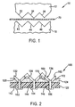
- a tooling fixture generally indicated at 10, includes an upper mold 12 and a lower mold 15.
- a copper foil sheet 20 is placed between the upper and lower mold as depicted in Figure 1.
- the upper mold 12 and the lower mold 15 have a plurality of mating corresponding concentric V-shaped surfaces 32, 34, 36 and 42, 42, 46, respectively. It should be understood that any configuration can be used other than v-shaped surfaces for electrical contact within the limits of material to be embossed.
- the copper foil sheet 20 is embossed or stamped with a plurality of concentric V-rings. Although three V-rings are depicted, it should be understood that this is for illustrative purposes only and any number of V-rings or grooves can be used.
- a rotor half, generally indicated at 100, usable with a pancake type slip ring is depicted.
- the rotor half 100 is depicted in a horizontal position, although it should be understood that the rotor half 100 is usable in any orientation.
- the rotor half 100 is usable in a pancake type slip ring as disclosed in U.S. Patent Application Serial No. 09/246,098, filed February 8, 1999 entitled “ELECTRICAL SLIP RING HAVING A HIGHER CIRCUIT DENSITY" and U.S. Patent No. 5,901,429 issued May 11, 1999 entitled “METHOD OF MANUFACTURING COMPOSITE PANCAKE SLIP RING ASSEMBLY", the disclosures of which are hereby incorporated by reference into this specification in their entirety.
- the rotor half 100 is formed from a dielectric layer 122, bonding agent 124 and the stamped copper foil sheet 120.
- the method of forming the rotor half 100 is as follows.
- the bonding agent 124 is placed upon one surface of the dielectric layer 122.
- the stamped copper foil sheet 120 is placed on the bonding agent 124.
- the stamped copper foil sheet 120 is placed on the bonding agent 124 and pressed into the bonding agent 124 such that the lower most apex of each of the V-rings is in contact with the upper surface of the dielectric layer 122.
- a machining operation is performed separating V-groove 132 from 134 and V-groove 134 from V-groove 136.
- the portion of the stamped copper foil sheet 120 removed between V-grooves 132, 134 and 136 is indicated with dashed lines.
- a corresponding bole 142, 144, 146 is drilled centrally through the V-groove in copper foil sheet 120 and through the dielectric layer 122.
- a copper foil trace 160 is bonded to a back side of the dielectric layer 122.
- a top half 162 of the copper foil trace 160 is not etched and a bottom half 164 is etched.
- a plurality of separate paths 182, 184, 186 are each connected to the rings 152, 154, 156, respectively, so that each conductive ring 132, 134, 136 can be electrically connected to an external electrical connection in a conventional manner. Any number of paths and rings can be used although three are depicted for simplicity.
- Two rotor halves 100 would be bonded together with the back sides bonded and the v-groove sides facing externally to form a rotor assembly.
- An electrically conductive material such as metalized epoxy which can be injected or troweled into holes 142-146 is then placed in each of the conductive holes.
- the assembled rotor 100 can then be assembled into a pancake type slip ring in a conventional manner.
Landscapes
- Engineering & Computer Science (AREA)
- Manufacturing & Machinery (AREA)
- Manufacture Of Motors, Generators (AREA)
- Induction Machinery (AREA)
- Motor Or Generator Current Collectors (AREA)
- Manufacturing Of Electrical Connectors (AREA)
Applications Claiming Priority (2)
| Application Number | Priority Date | Filing Date | Title |
|---|---|---|---|
| US404377 | 1999-09-24 | ||
| US09/404,377 US6222297B1 (en) | 1999-09-24 | 1999-09-24 | Pressed V-groove pancake slip ring |
Publications (2)
| Publication Number | Publication Date |
|---|---|
| EP1087473A2 true EP1087473A2 (fr) | 2001-03-28 |
| EP1087473A3 EP1087473A3 (fr) | 2002-07-10 |
Family
ID=23599358
Family Applications (1)
| Application Number | Title | Priority Date | Filing Date |
|---|---|---|---|
| EP00120581A Withdrawn EP1087473A3 (fr) | 1999-09-24 | 2000-09-20 | Bague collectrice plate comportant des rainures en forme de V |
Country Status (4)
| Country | Link |
|---|---|
| US (2) | US6222297B1 (fr) |
| EP (1) | EP1087473A3 (fr) |
| JP (1) | JP2001186725A (fr) |
| CA (1) | CA2320010A1 (fr) |
Families Citing this family (46)
| Publication number | Priority date | Publication date | Assignee | Title |
|---|---|---|---|---|
| US6356002B1 (en) * | 1999-02-08 | 2002-03-12 | Northrop Grumman Corporation | Electrical slip ring having a higher circuit density |
| US6984915B2 (en) * | 2002-01-22 | 2006-01-10 | Electro-Tec Corp. | Electrical slip ring platter multilayer printed circuit board and method for making same |
| US7071591B2 (en) * | 2003-01-02 | 2006-07-04 | Covi Technologies | Electromagnetic circuit and servo mechanism for articulated cameras |
| US20040169434A1 (en) * | 2003-01-02 | 2004-09-02 | Washington Richard G. | Slip ring apparatus |
| US6980714B2 (en) * | 2003-09-26 | 2005-12-27 | Moog Components Group Inc. | Fiber optic rotary joint and associated reflector assembly |
| US8497935B2 (en) | 2004-08-26 | 2013-07-30 | Robert Bosch Gmbh | Rotatable camera system including infrared communications links |
| US8414962B2 (en) | 2005-10-28 | 2013-04-09 | The Penn State Research Foundation | Microcontact printed thin film capacitors |
| GB0718706D0 (en) | 2007-09-25 | 2007-11-07 | Creative Physics Ltd | Method and apparatus for reducing laser speckle |
| US7750493B2 (en) * | 2007-08-14 | 2010-07-06 | General Electric Company | Wind turbine assemblies and slip ring assemblies for wind blade pitch control motors |
| US9335604B2 (en) | 2013-12-11 | 2016-05-10 | Milan Momcilo Popovich | Holographic waveguide display |
| US11726332B2 (en) | 2009-04-27 | 2023-08-15 | Digilens Inc. | Diffractive projection apparatus |
| US9274349B2 (en) | 2011-04-07 | 2016-03-01 | Digilens Inc. | Laser despeckler based on angular diversity |
| WO2016020630A2 (fr) | 2014-08-08 | 2016-02-11 | Milan Momcilo Popovich | Illuminateur laser en guide d'ondes comprenant un dispositif de déchatoiement |
| EP2748670B1 (fr) | 2011-08-24 | 2015-11-18 | Rockwell Collins, Inc. | Affichage de données portable |
| US20150010265A1 (en) | 2012-01-06 | 2015-01-08 | Milan, Momcilo POPOVICH | Contact image sensor using switchable bragg gratings |
| EP2842003B1 (fr) | 2012-04-25 | 2019-02-27 | Rockwell Collins, Inc. | Affichage grand angle holographique |
| US8993049B2 (en) * | 2012-08-09 | 2015-03-31 | Valinge Flooring Technology Ab | Single layer scattering of powder surfaces |
| US9933684B2 (en) | 2012-11-16 | 2018-04-03 | Rockwell Collins, Inc. | Transparent waveguide display providing upper and lower fields of view having a specific light output aperture configuration |
| JP6370029B2 (ja) * | 2013-03-13 | 2018-08-08 | 日東電工株式会社 | 粘着剤層付偏光フィルムおよび画像表示装置 |
| CN105393413B (zh) * | 2013-05-17 | 2019-01-04 | 史莱福灵有限公司 | 用于多纤维电刷的高电流滑环 |
| US9727772B2 (en) | 2013-07-31 | 2017-08-08 | Digilens, Inc. | Method and apparatus for contact image sensing |
| WO2016020632A1 (fr) | 2014-08-08 | 2016-02-11 | Milan Momcilo Popovich | Procédé pour gravure par pressage et réplication holographique |
| WO2016042283A1 (fr) | 2014-09-19 | 2016-03-24 | Milan Momcilo Popovich | Procédé et appareil de production d'images d'entrée pour affichages à guides d'ondes holographiques |
| US10437064B2 (en) | 2015-01-12 | 2019-10-08 | Digilens Inc. | Environmentally isolated waveguide display |
| US9632226B2 (en) | 2015-02-12 | 2017-04-25 | Digilens Inc. | Waveguide grating device |
| WO2017060665A1 (fr) | 2015-10-05 | 2017-04-13 | Milan Momcilo Popovich | Afficheur à guide d'ondes |
| JP6895451B2 (ja) | 2016-03-24 | 2021-06-30 | ディジレンズ インコーポレイテッド | 偏光選択ホログラフィー導波管デバイスを提供するための方法および装置 |
| EP3433658B1 (fr) | 2016-04-11 | 2023-08-09 | DigiLens, Inc. | Dispositif guide d'onde pour la projection de lumiere structuree |
| EP3548939A4 (fr) | 2016-12-02 | 2020-11-25 | DigiLens Inc. | Dispositif de guide d'ondes à éclairage de sortie uniforme |
| US10545346B2 (en) | 2017-01-05 | 2020-01-28 | Digilens Inc. | Wearable heads up displays |
| USD879402S1 (en) * | 2017-05-11 | 2020-03-24 | Curt G. Joa, Inc. | Elastic break brake |
| JP7456929B2 (ja) | 2018-01-08 | 2024-03-27 | ディジレンズ インコーポレイテッド | 導波管セルを製造するためのシステムおよび方法 |
| WO2019136476A1 (fr) | 2018-01-08 | 2019-07-11 | Digilens, Inc. | Architectures de guides d'ondes et procédés de fabrication associés |
| JP7404243B2 (ja) | 2018-01-08 | 2023-12-25 | ディジレンズ インコーポレイテッド | 導波管セル内のホログラフィック格子の高スループット記録のためのシステムおよび方法 |
| CN114721242B (zh) | 2018-01-08 | 2025-08-15 | 迪吉伦斯公司 | 用于制造光学波导的方法 |
| US11402801B2 (en) | 2018-07-25 | 2022-08-02 | Digilens Inc. | Systems and methods for fabricating a multilayer optical structure |
| WO2020149956A1 (fr) | 2019-01-14 | 2020-07-23 | Digilens Inc. | Affichage de guide d'ondes holographique avec couche de commande de lumière |
| US20200247017A1 (en) | 2019-02-05 | 2020-08-06 | Digilens Inc. | Methods for Compensating for Optical Surface Nonuniformity |
| US20220283377A1 (en) | 2019-02-15 | 2022-09-08 | Digilens Inc. | Wide Angle Waveguide Display |
| EP3924759B1 (fr) | 2019-02-15 | 2025-07-30 | Digilens Inc. | Procédés et appareils pour fournir un affichage de guide d'ondes holographique à l'aide de réseaux intégrés |
| JP2022525165A (ja) | 2019-03-12 | 2022-05-11 | ディジレンズ インコーポレイテッド | ホログラフィック導波管バックライトおよび関連する製造方法 |
| EP3980825A4 (fr) | 2019-06-07 | 2023-05-03 | Digilens Inc. | Guides d'ondes incorporant des réseaux transparents et réfléchissants et procédés de fabrication associés |
| JP2022543571A (ja) | 2019-07-29 | 2022-10-13 | ディジレンズ インコーポレイテッド | 画素化されたディスプレイの画像解像度および視野を乗算するための方法および装置 |
| JP2022546413A (ja) | 2019-08-29 | 2022-11-04 | ディジレンズ インコーポレイテッド | 真空回折格子および製造方法 |
| WO2022150841A1 (fr) | 2021-01-07 | 2022-07-14 | Digilens Inc. | Structures de réseau pour guides d'ondes de couleur |
| KR20230153459A (ko) | 2021-03-05 | 2023-11-06 | 디지렌즈 인코포레이티드. | 진공 주기적 구조체 및 제조 방법 |
Family Cites Families (19)
| Publication number | Priority date | Publication date | Assignee | Title |
|---|---|---|---|---|
| US1499622A (en) * | 1924-07-01 | Hermann markwalder | ||
| US3038138A (en) * | 1959-01-30 | 1962-06-05 | Engelhard Ind Inc | Collector ring assembly |
| US3246277A (en) * | 1962-06-04 | 1966-04-12 | Ronald W Sands | Electrical outlet device for rotatable elevativable chair |
| US3314038A (en) * | 1964-03-24 | 1967-04-11 | Donald E Rutten | Collector ring construction |
| US3210829A (en) * | 1964-11-02 | 1965-10-12 | Avco Corp | Method of making a switch stator |
| US3438123A (en) * | 1965-10-22 | 1969-04-15 | Dale Corp Van | Method of making a slip ring unit |
| US3594680A (en) * | 1968-10-23 | 1971-07-20 | Vandale Corp | Slipring unit |
| US4510276A (en) | 1979-12-13 | 1985-04-09 | Kollmorgen Technologies Corporation | Epoxy resin coating compositions for printed circuit boards |
| US4396850A (en) * | 1982-01-12 | 1983-08-02 | The Singer Company | Brush board assembly for dynamoelectric machine with flat end commutator |
| US4837920A (en) * | 1983-09-26 | 1989-06-13 | The Bfgoodrich Company | Slip ring assembly and method of manufacture |
| US4871935A (en) * | 1983-09-26 | 1989-10-03 | The B.F. Goodrich Company | Slip ring assembly and method of manufacture |
| US4705976A (en) * | 1986-04-30 | 1987-11-10 | National Machine Company, Inc. | Slip ring assembly and method of manufacture |
| US4782580A (en) * | 1986-04-30 | 1988-11-08 | National Machine Company, Inc. | Method of manufacture of slip ring assembly |
| GB2218861B (en) * | 1988-05-17 | 1992-04-22 | Gen Motors France | Alternator with cylindrical and flat slip-rings |
| US5925962A (en) * | 1995-12-19 | 1999-07-20 | Walbro Corporation | Electric motor commutator |
| US5734218A (en) | 1996-05-13 | 1998-03-31 | Litton Systems, Inc. | Electrical slip ring and method of manufacturing same |
| US5690498A (en) * | 1996-09-23 | 1997-11-25 | He Holdings, Inc | Spring loaded rotary connector |
| US5901429A (en) | 1997-07-03 | 1999-05-11 | Litton Systems, Inc. | Method of manufacturing composite pancake slip ring assembly |
| US6161275A (en) * | 1998-07-08 | 2000-12-19 | Siemens Canada Limited | Method of manufacturing commutators for electric motors |
-
1999
- 1999-09-24 US US09/404,377 patent/US6222297B1/en not_active Expired - Fee Related
-
2000
- 2000-09-18 JP JP2000281336A patent/JP2001186725A/ja not_active Withdrawn
- 2000-09-18 CA CA002320010A patent/CA2320010A1/fr not_active Abandoned
- 2000-09-20 EP EP00120581A patent/EP1087473A3/fr not_active Withdrawn
-
2001
- 2001-02-09 US US09/779,475 patent/US6536095B2/en not_active Expired - Fee Related
Also Published As
| Publication number | Publication date |
|---|---|
| EP1087473A3 (fr) | 2002-07-10 |
| CA2320010A1 (fr) | 2001-03-24 |
| US6222297B1 (en) | 2001-04-24 |
| US6536095B2 (en) | 2003-03-25 |
| US20010004176A1 (en) | 2001-06-21 |
| JP2001186725A (ja) | 2001-07-06 |
Similar Documents
| Publication | Publication Date | Title |
|---|---|---|
| EP1087473A2 (fr) | Bague collectrice plate comportant des rainures en forme de V | |
| KR100650614B1 (ko) | 다층기판 제조방법 | |
| US7383632B2 (en) | Method for fabricating a connector | |
| CA1048657A (fr) | Bande d'interconnexion de liaison pour dispositifs a semiconducteurs | |
| KR100433781B1 (ko) | 반도체장치의 제조방법 | |
| EP0236763A1 (fr) | Structure laminée d'enroulement imprimé | |
| US20040195581A1 (en) | Substrate for light emitting diodes | |
| EP1026794A3 (fr) | Bague collectrice à haute densité | |
| EP1357773A3 (fr) | Feuille de transfert de câblage et son procédé de fabrication, et panneau de câblage et son procédé de fabrication | |
| US5762845A (en) | Method of making circuit with conductive and non-conductive raised features | |
| US6085414A (en) | Method of making a flexible circuit with raised features protruding from two surfaces and products therefrom | |
| US5901429A (en) | Method of manufacturing composite pancake slip ring assembly | |
| US12217114B2 (en) | Lead-frame, card body of a smart card, smart card, and method of forming a smart card | |
| CN104364804B (zh) | 用于制造用于容纳半导体芯片的智能卡基体的方法和这样的智能卡基体 | |
| KR20080003802A (ko) | 반도체 장치 및 반도체 장치의 제조 방법 | |
| KR102913135B1 (ko) | 단면 냉각 파워 모듈 및 그 제조 방법 | |
| US20060285301A1 (en) | Method for making a pre-laminated inlet | |
| US20060030169A1 (en) | Sheet type connector and method of manufacturing the same | |
| US7915537B1 (en) | Interposer and method for making interposers | |
| CN222601493U (zh) | 电连接器 | |
| JP3117012B2 (ja) | 内部にもパッドを設けたカードエッジ型コネクタ及びその製造方法 | |
| JPS5821198Y2 (ja) | 印刷配線 | |
| JPH0446465B2 (fr) | ||
| JPH09199242A (ja) | プリント配線板一体型コネクタ及びその製造方法 | |
| CN117174652A (zh) | 玻璃芯基板制作方法及玻璃芯基板封装结构 |
Legal Events
| Date | Code | Title | Description |
|---|---|---|---|
| PUAI | Public reference made under article 153(3) epc to a published international application that has entered the european phase |
Free format text: ORIGINAL CODE: 0009012 |
|
| AK | Designated contracting states |
Kind code of ref document: A2 Designated state(s): AT BE CH CY DE DK ES FI FR GB GR IE IT LI LU MC NL PT SE |
|
| AX | Request for extension of the european patent |
Free format text: AL;LT;LV;MK;RO;SI |
|
| PUAL | Search report despatched |
Free format text: ORIGINAL CODE: 0009013 |
|
| AK | Designated contracting states |
Kind code of ref document: A3 Designated state(s): AT BE CH CY DE DK ES FI FR GB GR IE IT LI LU MC NL PT SE |
|
| AX | Request for extension of the european patent |
Free format text: AL;LT;LV;MK;RO;SI |
|
| 17P | Request for examination filed |
Effective date: 20030110 |
|
| AKX | Designation fees paid |
Designated state(s): AT BE CH CY DE DK ES FI FR GB GR IE IT LI LU MC NL PT SE |
|
| 17Q | First examination report despatched |
Effective date: 20030221 |
|
| GRAP | Despatch of communication of intention to grant a patent |
Free format text: ORIGINAL CODE: EPIDOSNIGR1 |
|
| STAA | Information on the status of an ep patent application or granted ep patent |
Free format text: STATUS: THE APPLICATION IS DEEMED TO BE WITHDRAWN |
|
| 18D | Application deemed to be withdrawn |
Effective date: 20041231 |