EP1087563A2 - System und Verfahren zur zuverlässigen Umschaltung zwischen redundanten Takten - Google Patents
System und Verfahren zur zuverlässigen Umschaltung zwischen redundanten Takten Download PDFInfo
- Publication number
- EP1087563A2 EP1087563A2 EP99120997A EP99120997A EP1087563A2 EP 1087563 A2 EP1087563 A2 EP 1087563A2 EP 99120997 A EP99120997 A EP 99120997A EP 99120997 A EP99120997 A EP 99120997A EP 1087563 A2 EP1087563 A2 EP 1087563A2
- Authority
- EP
- European Patent Office
- Prior art keywords
- clock
- line
- line divided
- divider
- divided
- Prior art date
- Legal status (The legal status is an assumption and is not a legal conclusion. Google has not performed a legal analysis and makes no representation as to the accuracy of the status listed.)
- Granted
Links
Images


Classifications
-
- H—ELECTRICITY
- H04—ELECTRIC COMMUNICATION TECHNIQUE
- H04L—TRANSMISSION OF DIGITAL INFORMATION, e.g. TELEGRAPHIC COMMUNICATION
- H04L12/00—Data switching networks
- H04L12/28—Data switching networks characterised by path configuration, e.g. LAN [Local Area Networks] or WAN [Wide Area Networks]
-
- H—ELECTRICITY
- H04—ELECTRIC COMMUNICATION TECHNIQUE
- H04J—MULTIPLEX COMMUNICATION
- H04J3/00—Time-division multiplex systems
- H04J3/02—Details
- H04J3/06—Synchronising arrangements
- H04J3/0635—Clock or time synchronisation in a network
- H04J3/0685—Clock or time synchronisation in a node; Intranode synchronisation
- H04J3/0688—Change of the master or reference, e.g. take-over or failure of the master
-
- H—ELECTRICITY
- H04—ELECTRIC COMMUNICATION TECHNIQUE
- H04L—TRANSMISSION OF DIGITAL INFORMATION, e.g. TELEGRAPHIC COMMUNICATION
- H04L1/00—Arrangements for detecting or preventing errors in the information received
- H04L1/22—Arrangements for detecting or preventing errors in the information received using redundant apparatus to increase reliability
Definitions
- the present invention relates generally to digital switching networks. More particularly, the present invention relates to a system and method for preventing time-walking when switching between redundant clocks in a digital switching network.
- a system clock can be used to drive multiple modules.
- the system clock can also provide a synchronization pulse to each module it drives thus enabling the modules to communicate with each other. If the clock fails for any reason, the digital switching network switches to a redundant clock to avoid any interruption in communication between the modules. However, data can be lost in some digital switching networks due to a scenario called time-walking.
- Time-walking can occur if two clocks, independent in phase and fixed to the same frequency, are repeatedly switched to be the selected clock. Time-walking steps the time base of occurrence for the synchronous circuitry within the digital switching network which uses the selected clock. If time-walking is not prevented, it can occur that data will no longer be reliably switched throughout the digital switching network without reconfiguration. An example of the time walking scenario is further explained below in FIGURES 1 through 3.
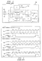
- FIGURE 1 shows the block diagram of a prior art digital switching network 100.
- the prior art digital switching network 100 is comprised of clock one 105, clock two 110, selector circuit A 120, selector circuit B 125, module A 130, module B 135, and module C 140.
- Selector circuit A 120 and selector circuit B 125 switch between clock one 105 and clock two 110 when either clock fails.
- module A 130, module B 135, and module C 140 are simple eight (8) state counters that produce a pulse on the eighth state.
- Module A 130 and module B 135 pass data between each other.
- Module C 140 provides a steady state reference while selector circuit A 120 and selector circuit B 125 switch between clock one 105 and clock two 110.
- a delay 115 is between clock two 110 and selector circuit A 120.
- clock one 105 and clock two 110 at selector circuit A 120 are not in phase.
- clock one 105 and clock two 110 at selector circuit B 125 are in phase.
- Module C 140 is driven only by clock one 105.
- FIGURE 2 shows the timing diagram at selector circuit A 205, the timing diagram at selector circuit B 210, and the timing diagram at module C 215 under steady state conditions (i.e. no switching between clock one 105 and clock two 110 at selector circuit A 120 or selector circuit B 125).
- clock one 105 and clock two 110 are identical in frequency. Since no switching occurs and clock one 105 is in phase at selector circuit A 120, at selector circuit B 125, and at module C 140, no time-walking will occur.
- FIGURE 3 shows the timing diagram at selector circuit A 305, the timing diagram at selector circuit B 310, and the timing diagram at module C 315 where selector circuit A 120 and selector circuit B 125 switch from clock one 105 to clock two 110 and back to clock one 105 again.
- clock one 105 and clock two 110 are identical in frequency, however, the timing diagram at selector circuit A 305 shows that clock one 105 and clock two 110 are not in phase due to the delay 115.
- the selector circuit A 120 does not take into account the phase difference between clock one 105 and clock two 110, the module A pulse 145 will walk in time relative the module B pulse 150 and module C pulse 155 as shown in FIGURE 3. This time-walking scenario can cause data passing between module A 130 and module B 135 to be lost. More data will continue to be lost if selector circuit A 120 continues to switch between clock one 105 and clock two 110.
- the present invention provides a system and method that substantially eliminates or reduces disadvantages and problems associated with previously developed systems and methods used for preventing time-walking in a digital switching network. More specifically, the present invention provides a system for preventing time-walking in a digital switching network when switching between redundant clocks identical in frequency and independent in phase, where the highest resolution frequency available in the digital switching network is that of the redundant clocks.
- the system for preventing time-walking in a digital switching network includes a clock divider selection circuit, an enhanced digital phase aligner, and a clock select control circuit.
- the clock divider selection circuit outputs an on-line divided clock and an off-line clock to the enhanced digital phase aligner.
- the enhanced digital phase aligner can sample the on-line divided clock with four phases of the off-line clock and outputs an off-line divided clock which is time shifted such that the off-line divided clock is in phase with the on-line divided clock within plus or minus one-half the clock period of the off-line clock.
- the clock select control circuit receives the on-line divided clock from the clock divider selection circuit, the off-line divided clock from the enhanced digital phase aligner, and a smoothed clock. When a request is made to switch between a first clock and a second clock, the clock select control circuit compares the on-line divided clock and the off-line divided clock with the smoothed clock and outputs a clock select control signal to the clock divider selection circuit.
- the present invention provides an important technical advantage by providing a system and method for preventing time-walking in a digital switching network when switching between redundant clocks which are identical in frequency but independent in phase.
- the present invention provides another technical advantage by providing a more stable environment so customer data can be more reliably switched throughout a digital switching network, thus saving the customer money.
- FIGUREs Preferred embodiments of the present invention are illustrated in the FIGUREs, like numerals being used to refer to like and corresponding parts of the various drawings.
- the present invention provides a system and method for preventing time-walking in a digital switching network when switching from a first clock to a second clock where said first and second clock are identical in frequency, independent in phase, and the highest resolution frequency available is that of said first and second clock.
- the present invention can include a clock divider selection circuit, an enhanced digital phase aligner, and a clock select control circuit.
- the system for preventing time-walking in a digital switching network includes a clock divider selection circuit, an enhanced digital phase aligner, and a clock select control circuit.
- the clock divider selection circuit outputs an on-line divided clock and an off-line clock to the enhanced digital phase aligner.
- the enhanced digital phase aligner samples the on-line divided clock with four phases of the off-line clock and outputs an off-line divided clock which is time shifted such that the off-line divided clock is in phase with the on-line divided clock within plus or minus one-half the clock period of the off-line clock.
- the clock select control circuit receives the on-line divided clock from the clock divider selection circuit, the off-line divided clock from the enhanced digital phase aligner, and a smoothed clock. When a request is made to switch between a first clock and a second clock, the clock select control circuit compares the on-line divided clock and the off-line divided clock with the smoothed clock and outputs a clock select control signal to the clock divider selection circuit.
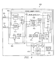
- FIGURE 4 shows one example of a circuit which prevents time-walking in a digital switching network during clock selection according to the present invention 400.
- the time-walking prevention circuit 400 includes a clock divider selection circuit 405, an enhanced digital phase aligner 440, a phase lock loop 470, a clock select control circuit 475, and a clock divider jamming circuit 490.
- the clock divider selection circuit 405 includes a first clock divider circuit 410, a second clock divider circuit 415, a first multiplexer 420, and a second multiplexer 425.
- the clock divider jamming circuit 490 includes a third multiplexer 450 and a fourth multiplexer 455.
- the first and second clock divider circuits 410 and 415 are divide by eight (8) divider circuits, however, other sized divider circuits may be used.
- the first, second, third and fourth multiplexers 420, 425, 450, and 455, respectively are 2:1 multiplexers, however, other sizes may be used.
- the clock divider selection circuit 405 receives a first clock 105 and a second clock 110 which are out of phase with respect to one another.
- the first clock 105 is input into the first clock divider circuit 410 and immediately gets divided by eight (8).
- the second clock 110 is input into the second clock divider circuit 415 and immediately gets divided by eight (8).
- the first clock 105 and the second clock 110 also are input into the first multiplexer 420.
- the first multiplexer 420 and the second multiplexer 425 receive a clock select control signal 480 from the clock select control circuit 475.
- the first multiplexer 420 outputs either the first clock 105 or the second clock 110 to the enhanced digital phase aligner 440 as the off-line clock 435 based on the clock select control signal 480.
- the second multiplexer 425 outputs either the divided first clock or the divided second clock to the enhanced digital phase aligner 440 as the on-line divided clock 430 based on the clock select control signal 480.
- the divided first clock is selected as the on-line divided clock 430 and the second clock 110 is selected as the off-line clock 435.
- the purpose of the enhanced digital phase aligner 440 is to pass the on-line divided clock 430 to the off-line regime.
- the enhanced digital phase aligner 440 receives the on-line divided clock 430 from the clock divider selection circuit 405, receives the off-line clock 435 from the clock divider selection circuit 405, and outputs an off-line divided clock 445 which is time shifted such that the off-line divided clock 445 is in phase with the on-line divided clock 430 within plus or minus one-half the clock period of the off-line clock 420.
- the off-line divided clock 445 is output from the enhanced digital phase aligner 440, it is input into the clock select control circuit 475.
- the clock select control circuit 475 also receives the on-line divided clock 430 from the clock divider selection circuit 405 and a smoothed clock 485 from the phase lock loop 470. Once a request is made to switch between the first clock 105 and the second clock 110, the clock select control circuit 475 evaluates the on-line divided clock 430 and the off-line divided clock 445 with the smoothed clock 485 and outputs a clock select control signal 480 to the first multiplexer 420 and the second multiplexer 425 in the clock divider selection circuit 405.
- the first multiplexer 420 selects either the first clock 105 or the second clock 110 as the off-line clock 435 based on the clock select control signal 480.
- the second multiplexer 425 selects either the first divided clock or the second divided clock as the on-line divided clock 430 based on the clock select control signal 480.
- the off-line divided clock 445 is also output to the clock divider jamming circuit 490.
- the clock divider jamming circuit 490 also receives the on-line divided clock 430 from the clock divider selection circuit 405 and the clock select control signal 480 from the clock select control circuit 475.
- the clock selection control signal 480, the off-line divided clock 445, and the on-line divided clock 430 are each input into the third multiplexer 450 and the fourth multiplexer 455.
- the third multiplexer 450 outputs either the on-line divided clock 430 or the off-line divided clock 445 as the first clock divider jamming signal 460 based on the clock select control signal 480.
- the fourth multiplexer 455 outputs either the on-line divided clock 430 or the off-line divided clock 445 as the second clock divider jamming signal 465 based on the clock select control signal 480.
- the first clock divider jamming signal 460 is fed back to the first clock divider circuit 410 located in the clock divider selection circuit 405.
- the second clock divider jamming signal 465 is fed back to the second clock divider circuit 415 located in the clock divider selection circuit 405.
- the purpose of the first and second clock divider jamming signals 460 and 465, respectively, is to jam the first and second clock divider circuits 410 and 415, respectively so that both the first clock divider circuit 410 and the second clock divider circuit 415 output divided signals that look exactly the same except for the phase shift which is equal to the same phase shift as between the first clock 105 and the second clock 110.
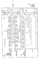
- FIGURE 5 shows one example of the circuitry for the enhanced digital phase aligner 440 according to the present invention.
- the enhanced digital phase aligner 440 includes a clock generator 505, a phase analyzer 510, and a time shifter 515.
- the phase analyzer 510 includes a data sampler 520, a control circuit 525, a counter 530, a first flip flop 535, a second flip flop 540, a first serial shift register 545, a second serial shift register 550 a fifth multiplexer 555, and a third flip flop 560.
- the first and second serial shift registers, 545 and 550 are 1:8 serial shift registers
- the counter 530 is a four (4) bit counter
- the fifth multiplexer is a 16:1 multiplexer, however, other sizes may be used.
- the clock generator 505 receives the off-line clock 435 from the said clock divider selection circuit, generates four phases of the off-line clock 435, and inputs the four phases into the phase analyzer 510.
- the four phases produced are 0, 90, 180, and 270 degrees. Other phases may be produced.
- FIGURE 6 shows a timing diagram of the four phases. After entering the phase analyzer 510, the four phases are first received at the data sampler 520. The on-line divided clock 430 is also received at the data sampler 520. The data sampler 520 uses the four phases of the off-line clock 435 to sample the on-line divided clock 430 and outputs multiple data samples of the on-line divided clock 430 to the control circuit 525.
- the control circuit 525 analyzes the multiple data samples from the data sampler 520 and selects the phase of the off-line clock which is the furthest from the leading edge of the on-line divided clock 430. When ever the currently selected sample point gets closer than ninety (90) degrees to a data transition, the output sample is changed by one hundred eighty (180) degrees. This is done by sending a signal from the control circuit 525 to the counter 530 which either increments or decrements the counter 530. Once the counter 530 is either incremented or decremented, the counter 530 sends a phase select control signal 470 to the fifth multiplexer 555 which then adjusts the sample one hundred eighty (180) degrees based on the count value. If the count roles over (i.e. 0000 to 1111 or 1111 to 0000), a spill will be indicated by outputting a spill signal 465 from the counter 530. The phase select control signal 470 is also output to the time shifter 515.
- FIGURE 7 shows one example of the time shifter 515 circuit according to the present invention.
- the time shifter 515 includes a multiplexer 705, a tapped shift register 710, and a flip flop 715.
- the time shifter 515 receives the off-line clock 435 from the clock divider selection circuit 405, the sampled on-line divided clock 475 from the phase analyzer 510 and the phase select control signal 470 from the phase analyzer 515.
- the purpose of time shifter 515 is to time shift the off-line divided clock 445 such that the off-line divided clock 445 is in phase with the on-line divided clock 430 within plus or minus one-half the clock period of the off-line clock 435.
- the selection on the multiplexer 705 is based upon the count value of the counter 530. That information is carried from the counter 530 to the multiplexer 705 through the phase select control signal 470. The three least significant bits of the count value are used to determine how much delay needs to be added to the sampled on-line divided clock 470 so that the edges of the off-line divided clock 445 are as close as possible to the edges of the on-line divided clock 430.
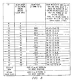
- TABLE 1 shows a table that describes how much delay is needed to time shift the sampled on-line divided clock 475.
- the Flip Flop column there is A and C. If C0 is selected, less than one period will need to be added to the sampled on-line divided clock 475. In the last column, 48 nanoseconds represents the total period. First, the 12 nanoseconds that C0 adds is subtracted, next the 12 nanoseconds that the flip flop 715 adds is subtracted, finally the 6 seconds that flip flop C adds is subtracted. Thus 18 nanoseconds is needed to time shift the off-line divided clock 445 such that the off-line divided clock 445 is in phase with the on-line divided clock 430 within plus or minus one-half the clock period of the off-line clock 435. The tapped shift register 710 will then tap off of the third flip flop in the tapped shift register 710 since each flip flop in the tapped shift register 710 has a delay of 6.
- FIGURE 8 shows one example of the clock select control circuit 475.
- the clock select control circuit includes a multiplexer 905 and multiple flip flops 910.
- the on-line divided clock 430 and the off-line divided clock 445 are input into the multiplexer 905.
- the smoothed clock 485 is input into the multiplexer 905 and in each flip flop 910.
- FIGURE 9 shows a clock control timing diagram 1000 which details the two times when the first clock 105 can switch to the second clock 110 or when the second clock 110 can switch to the first clock 105.
- the clock select control circuit 475 compares said on-line divided clock and said off-line divided clock to said smoothed clock and determines whether the request falls in either the first switch time 1005 or the second switch time 1010. Next, the clock select control circuit 475 sends out a clock select control signal to the clock divider select circuit and the clock divider jamming circuit.
- the present invention provides a system and method for preventing time-walking in a digital switching network when switching from a first clock to a second clock where said first and second clock are identical in frequency, independent in phase, and the highest resolution frequency available is that of said first and second clock includes a clock divider selection circuit, an enhanced digital phase aligner, and a clock select control circuit.
- the clock divider selection circuit outputs an on-line divided clock and an off-line clock to the enhanced digital phase aligner.
- the enhanced digital phase aligner samples the on-line divided clock with four phases of the off-line clock and outputs an off-line divided clock which is time shifted such that the off-line divided clock is in phase with the on-line divided clock within plus or minus one-half the clock period of the off-line clock.
- the clock select control circuit receives the on-line divided clock from the clock divider selection circuit, the off-line divided clock from the enhanced digital phase aligner and a smoothed clock. When a request is made to switch between clock one and clock two, the clock select control circuit evaluates the on-line divided clock and the off-line divided clock with the smoothed clock and outputs a clock select control signal to the clock divider selection circuit.
Landscapes
- Engineering & Computer Science (AREA)
- Computer Networks & Wireless Communication (AREA)
- Signal Processing (AREA)
- Synchronisation In Digital Transmission Systems (AREA)
- Stabilization Of Oscillater, Synchronisation, Frequency Synthesizers (AREA)
- Detection And Prevention Of Errors In Transmission (AREA)
- Time-Division Multiplex Systems (AREA)
- Circuits Of Receivers In General (AREA)
- Mobile Radio Communication Systems (AREA)
Applications Claiming Priority (2)
| Application Number | Priority Date | Filing Date | Title |
|---|---|---|---|
| US399711 | 1999-09-21 | ||
| US09/399,711 US6194939B1 (en) | 1999-09-21 | 1999-09-21 | Time-walking prevention in a digital switching implementation for clock selection |
Publications (3)
| Publication Number | Publication Date |
|---|---|
| EP1087563A2 true EP1087563A2 (de) | 2001-03-28 |
| EP1087563A3 EP1087563A3 (de) | 2004-03-31 |
| EP1087563B1 EP1087563B1 (de) | 2007-01-17 |
Family
ID=23580674
Family Applications (1)
| Application Number | Title | Priority Date | Filing Date |
|---|---|---|---|
| EP99120997A Expired - Lifetime EP1087563B1 (de) | 1999-09-21 | 1999-11-04 | System und Verfahren zur zuverlässigen Umschaltung zwischen redundanten Takten |
Country Status (10)
| Country | Link |
|---|---|
| US (1) | US6194939B1 (de) |
| EP (1) | EP1087563B1 (de) |
| KR (1) | KR20010029434A (de) |
| AT (1) | ATE352141T1 (de) |
| AU (1) | AU6538399A (de) |
| CA (1) | CA2287588A1 (de) |
| DE (1) | DE69934886T2 (de) |
| IL (1) | IL132476A0 (de) |
| SG (1) | SG97133A1 (de) |
| TW (1) | TW432802B (de) |
Cited By (1)
| Publication number | Priority date | Publication date | Assignee | Title |
|---|---|---|---|---|
| US10396922B2 (en) * | 2017-02-07 | 2019-08-27 | Texas Instruments Incorporated | Apparatus and mechanism to support multiple time domains in a single soc for time sensitive network |
Families Citing this family (8)
| Publication number | Priority date | Publication date | Assignee | Title |
|---|---|---|---|---|
| DE19954696A1 (de) * | 1999-11-13 | 2001-05-17 | Philips Corp Intellectual Pty | Telekommunikationsgerät mit einer Taktgenerierungseinheit |
| GB2358531B (en) * | 2000-01-18 | 2003-06-04 | 3Com Corp | Glitch free clock multiplexer circuit |
| US6411130B1 (en) * | 2001-01-23 | 2002-06-25 | Micrel, Inc. | Method and system for reliably providing a lock indication |
| US6441656B1 (en) * | 2001-07-31 | 2002-08-27 | Sun Microsystems, Inc. | Clock divider for analysis of all clock edges |
| US6891401B2 (en) * | 2001-08-03 | 2005-05-10 | Altera Corporation | Clock loss detection and switchover circuit |
| US6856925B2 (en) * | 2001-10-26 | 2005-02-15 | Texas Instruments Incorporated | Active removal of aliasing frequencies in a decimating structure by changing a decimation ratio in time and space |
| US6839391B2 (en) * | 2002-01-08 | 2005-01-04 | Motorola, Inc. | Method and apparatus for a redundant clock |
| KR20040083870A (ko) * | 2003-03-25 | 2004-10-06 | 유티스타콤코리아 유한회사 | 클럭 보드 이중화 방법 |
Family Cites Families (9)
| Publication number | Priority date | Publication date | Assignee | Title |
|---|---|---|---|---|
| US4651103A (en) * | 1985-12-30 | 1987-03-17 | At&T Company | Phase adjustment system |
| JPH04113718A (ja) * | 1990-09-04 | 1992-04-15 | Fujitsu Ltd | ヒットレス・クロック切替装置 |
| US5059925A (en) * | 1990-09-28 | 1991-10-22 | Stratacom, Inc. | Method and apparatus for transparently switching clock sources |
| US5638410A (en) * | 1993-10-14 | 1997-06-10 | Alcatel Network Systems, Inc. | Method and system for aligning the phase of high speed clocks in telecommunications systems |
| US5533072A (en) * | 1993-11-12 | 1996-07-02 | International Business Machines Corporation | Digital phase alignment and integrated multichannel transceiver employing same |
| KR0177731B1 (ko) * | 1994-09-15 | 1999-05-15 | 정장호 | 망동기용 디지탈 위상동기루프 제어방법 |
| US5623223A (en) * | 1994-10-12 | 1997-04-22 | National Semiconductor Corporation | Glitchless clock switching circuit |
| US5920600A (en) * | 1995-09-18 | 1999-07-06 | Oki Electric Industry Co., Ltd. | Bit phase synchronizing circuitry for controlling phase and frequency, and PLL circuit therefor |
| US5652536A (en) * | 1995-09-25 | 1997-07-29 | Cirrus Logic, Inc. | Non-glitch clock switching circuit |
-
1999
- 1999-09-21 US US09/399,711 patent/US6194939B1/en not_active Expired - Lifetime
- 1999-10-20 IL IL13247699A patent/IL132476A0/xx unknown
- 1999-10-25 CA CA002287588A patent/CA2287588A1/en not_active Abandoned
- 1999-11-04 AT AT99120997T patent/ATE352141T1/de not_active IP Right Cessation
- 1999-11-04 DE DE69934886T patent/DE69934886T2/de not_active Expired - Lifetime
- 1999-11-04 SG SG9905473A patent/SG97133A1/en unknown
- 1999-11-04 EP EP99120997A patent/EP1087563B1/de not_active Expired - Lifetime
- 1999-12-14 TW TW088121911A patent/TW432802B/zh not_active IP Right Cessation
- 1999-12-20 KR KR1019990059161A patent/KR20010029434A/ko not_active Withdrawn
- 1999-12-21 AU AU65383/99A patent/AU6538399A/en not_active Abandoned
Cited By (1)
| Publication number | Priority date | Publication date | Assignee | Title |
|---|---|---|---|---|
| US10396922B2 (en) * | 2017-02-07 | 2019-08-27 | Texas Instruments Incorporated | Apparatus and mechanism to support multiple time domains in a single soc for time sensitive network |
Also Published As
| Publication number | Publication date |
|---|---|
| DE69934886T2 (de) | 2007-11-08 |
| US6194939B1 (en) | 2001-02-27 |
| AU6538399A (en) | 2001-03-22 |
| SG97133A1 (en) | 2003-07-18 |
| IL132476A0 (en) | 2001-03-19 |
| CA2287588A1 (en) | 2001-03-21 |
| EP1087563A3 (de) | 2004-03-31 |
| EP1087563B1 (de) | 2007-01-17 |
| DE69934886D1 (de) | 2007-03-08 |
| TW432802B (en) | 2001-05-01 |
| KR20010029434A (ko) | 2001-04-06 |
| ATE352141T1 (de) | 2007-02-15 |
Similar Documents
| Publication | Publication Date | Title |
|---|---|---|
| US5675274A (en) | Semiconductor clock signal generation circuit | |
| US4119796A (en) | Automatic data synchronizer | |
| EP1166210B1 (de) | Elastische schnittstelleanornung und verfahren dafür | |
| EP0711472B1 (de) | Verfahren und Vorrichtung zur Phasenverschiebung eines Taktsignals | |
| EP0903885B1 (de) | Taktrückgewinnungsschaltung | |
| US6104228A (en) | Phase aligner system and method | |
| US5689530A (en) | Data recovery circuit with large retime margin | |
| US7453970B2 (en) | Clock signal selecting apparatus and method that guarantee continuity of output clock signal | |
| US6341149B1 (en) | Clock control device for a non-disruptive backup clock switching | |
| US6194939B1 (en) | Time-walking prevention in a digital switching implementation for clock selection | |
| US6956415B2 (en) | Modular DLL architecture for generating multiple timings | |
| JP3294566B2 (ja) | ビット位相同期装置 | |
| EP0379279A2 (de) | Datenvermittlungssynchronisator | |
| JPH0614638B2 (ja) | 局部クロック信号と受信データ信号とを再同期させる機構 | |
| US5371416A (en) | Circuit and method of synchronizing clock signals | |
| US6996201B2 (en) | Data receiving system robust against jitter of clock | |
| US5844908A (en) | Digital delay system and method for digital cross connect telecommunication systems | |
| US20040095166A1 (en) | Clock switching circuit | |
| JP3006550B2 (ja) | クロック調整回路 | |
| JP2744094B2 (ja) | ディジタルシステム | |
| JPH0897750A (ja) | クロック受信分配システム | |
| US5822332A (en) | Pseudonoise code pull in circuit | |
| JP3132657B2 (ja) | クロック切替回路 | |
| JPH01296734A (ja) | クロック、データ信号の位相同期回路 | |
| JPH11205101A (ja) | 位相追従装置 |
Legal Events
| Date | Code | Title | Description |
|---|---|---|---|
| PUAI | Public reference made under article 153(3) epc to a published international application that has entered the european phase |
Free format text: ORIGINAL CODE: 0009012 |
|
| AK | Designated contracting states |
Kind code of ref document: A2 Designated state(s): AT BE CH CY DE DK ES FI FR GB GR IE IT LI LU MC NL PT SE |
|
| AX | Request for extension of the european patent |
Free format text: AL;LT;LV;MK;RO;SI |
|
| PUAL | Search report despatched |
Free format text: ORIGINAL CODE: 0009013 |
|
| AK | Designated contracting states |
Kind code of ref document: A3 Designated state(s): AT BE CH CY DE DK ES FI FR GB GR IE IT LI LU MC NL PT SE |
|
| AX | Request for extension of the european patent |
Extension state: AL LT LV MK RO SI |
|
| RIC1 | Information provided on ipc code assigned before grant |
Ipc: 7H 04L 7/033 B Ipc: 7H 04J 3/06 B Ipc: 7H 04L 1/22 A |
|
| 17P | Request for examination filed |
Effective date: 20040924 |
|
| AKX | Designation fees paid |
Designated state(s): AT BE CH CY DE DK ES FI FR GB GR IE IT LI LU MC NL PT SE |
|
| 17Q | First examination report despatched |
Effective date: 20050701 |
|
| GRAP | Despatch of communication of intention to grant a patent |
Free format text: ORIGINAL CODE: EPIDOSNIGR1 |
|
| GRAS | Grant fee paid |
Free format text: ORIGINAL CODE: EPIDOSNIGR3 |
|
| GRAA | (expected) grant |
Free format text: ORIGINAL CODE: 0009210 |
|
| AK | Designated contracting states |
Kind code of ref document: B1 Designated state(s): AT BE CH CY DE DK ES FI FR GB GR IE IT LI LU MC NL PT SE |
|
| PG25 | Lapsed in a contracting state [announced via postgrant information from national office to epo] |
Ref country code: NL Free format text: LAPSE BECAUSE OF FAILURE TO SUBMIT A TRANSLATION OF THE DESCRIPTION OR TO PAY THE FEE WITHIN THE PRESCRIBED TIME-LIMIT Effective date: 20070117 Ref country code: LI Free format text: LAPSE BECAUSE OF FAILURE TO SUBMIT A TRANSLATION OF THE DESCRIPTION OR TO PAY THE FEE WITHIN THE PRESCRIBED TIME-LIMIT Effective date: 20070117 Ref country code: FI Free format text: LAPSE BECAUSE OF FAILURE TO SUBMIT A TRANSLATION OF THE DESCRIPTION OR TO PAY THE FEE WITHIN THE PRESCRIBED TIME-LIMIT Effective date: 20070117 Ref country code: DK Free format text: LAPSE BECAUSE OF FAILURE TO SUBMIT A TRANSLATION OF THE DESCRIPTION OR TO PAY THE FEE WITHIN THE PRESCRIBED TIME-LIMIT Effective date: 20070117 Ref country code: CH Free format text: LAPSE BECAUSE OF FAILURE TO SUBMIT A TRANSLATION OF THE DESCRIPTION OR TO PAY THE FEE WITHIN THE PRESCRIBED TIME-LIMIT Effective date: 20070117 Ref country code: AT Free format text: LAPSE BECAUSE OF FAILURE TO SUBMIT A TRANSLATION OF THE DESCRIPTION OR TO PAY THE FEE WITHIN THE PRESCRIBED TIME-LIMIT Effective date: 20070117 |
|
| REG | Reference to a national code |
Ref country code: GB Ref legal event code: FG4D |
|
| REG | Reference to a national code |
Ref country code: CH Ref legal event code: EP |
|
| REG | Reference to a national code |
Ref country code: IE Ref legal event code: FG4D |
|
| REF | Corresponds to: |
Ref document number: 69934886 Country of ref document: DE Date of ref document: 20070308 Kind code of ref document: P |
|
| PG25 | Lapsed in a contracting state [announced via postgrant information from national office to epo] |
Ref country code: SE Free format text: LAPSE BECAUSE OF FAILURE TO SUBMIT A TRANSLATION OF THE DESCRIPTION OR TO PAY THE FEE WITHIN THE PRESCRIBED TIME-LIMIT Effective date: 20070417 |
|
| PG25 | Lapsed in a contracting state [announced via postgrant information from national office to epo] |
Ref country code: ES Free format text: LAPSE BECAUSE OF FAILURE TO SUBMIT A TRANSLATION OF THE DESCRIPTION OR TO PAY THE FEE WITHIN THE PRESCRIBED TIME-LIMIT Effective date: 20070428 |
|
| RAP2 | Party data changed (patent owner data changed or rights of a patent transferred) |
Owner name: ALCATEL LUCENT |
|
| PG25 | Lapsed in a contracting state [announced via postgrant information from national office to epo] |
Ref country code: PT Free format text: LAPSE BECAUSE OF FAILURE TO SUBMIT A TRANSLATION OF THE DESCRIPTION OR TO PAY THE FEE WITHIN THE PRESCRIBED TIME-LIMIT Effective date: 20070618 |
|
| NLT2 | Nl: modifications (of names), taken from the european patent patent bulletin |
Owner name: ALCATEL LUCENT Effective date: 20070502 |
|
| NLV1 | Nl: lapsed or annulled due to failure to fulfill the requirements of art. 29p and 29m of the patents act | ||
| REG | Reference to a national code |
Ref country code: CH Ref legal event code: PL |
|
| ET | Fr: translation filed | ||
| PLBE | No opposition filed within time limit |
Free format text: ORIGINAL CODE: 0009261 |
|
| STAA | Information on the status of an ep patent application or granted ep patent |
Free format text: STATUS: NO OPPOSITION FILED WITHIN TIME LIMIT |
|
| 26N | No opposition filed |
Effective date: 20071018 |
|
| PG25 | Lapsed in a contracting state [announced via postgrant information from national office to epo] |
Ref country code: BE Free format text: LAPSE BECAUSE OF FAILURE TO SUBMIT A TRANSLATION OF THE DESCRIPTION OR TO PAY THE FEE WITHIN THE PRESCRIBED TIME-LIMIT Effective date: 20070117 |
|
| PG25 | Lapsed in a contracting state [announced via postgrant information from national office to epo] |
Ref country code: GR Free format text: LAPSE BECAUSE OF FAILURE TO SUBMIT A TRANSLATION OF THE DESCRIPTION OR TO PAY THE FEE WITHIN THE PRESCRIBED TIME-LIMIT Effective date: 20070418 |
|
| PG25 | Lapsed in a contracting state [announced via postgrant information from national office to epo] |
Ref country code: MC Free format text: LAPSE BECAUSE OF NON-PAYMENT OF DUE FEES Effective date: 20071130 |
|
| PGFP | Annual fee paid to national office [announced via postgrant information from national office to epo] |
Ref country code: IE Payment date: 20081124 Year of fee payment: 10 |
|
| PG25 | Lapsed in a contracting state [announced via postgrant information from national office to epo] |
Ref country code: CY Free format text: LAPSE BECAUSE OF FAILURE TO SUBMIT A TRANSLATION OF THE DESCRIPTION OR TO PAY THE FEE WITHIN THE PRESCRIBED TIME-LIMIT Effective date: 20070117 |
|
| PG25 | Lapsed in a contracting state [announced via postgrant information from national office to epo] |
Ref country code: LU Free format text: LAPSE BECAUSE OF NON-PAYMENT OF DUE FEES Effective date: 20071104 |
|
| PG25 | Lapsed in a contracting state [announced via postgrant information from national office to epo] |
Ref country code: IE Free format text: LAPSE BECAUSE OF NON-PAYMENT OF DUE FEES Effective date: 20091104 |
|
| REG | Reference to a national code |
Ref country code: FR Ref legal event code: GC Effective date: 20140717 |
|
| REG | Reference to a national code |
Ref country code: FR Ref legal event code: RG Effective date: 20141016 |
|
| REG | Reference to a national code |
Ref country code: FR Ref legal event code: CA Effective date: 20150521 |
|
| REG | Reference to a national code |
Ref country code: FR Ref legal event code: CA Effective date: 20150521 |
|
| REG | Reference to a national code |
Ref country code: FR Ref legal event code: PLFP Year of fee payment: 17 |
|
| REG | Reference to a national code |
Ref country code: FR Ref legal event code: PLFP Year of fee payment: 18 |
|
| PGFP | Annual fee paid to national office [announced via postgrant information from national office to epo] |
Ref country code: FR Payment date: 20161118 Year of fee payment: 18 |
|
| PGFP | Annual fee paid to national office [announced via postgrant information from national office to epo] |
Ref country code: IT Payment date: 20161123 Year of fee payment: 18 |
|
| PGFP | Annual fee paid to national office [announced via postgrant information from national office to epo] |
Ref country code: DE Payment date: 20171121 Year of fee payment: 19 |
|
| PGFP | Annual fee paid to national office [announced via postgrant information from national office to epo] |
Ref country code: GB Payment date: 20171123 Year of fee payment: 19 |
|
| REG | Reference to a national code |
Ref country code: FR Ref legal event code: ST Effective date: 20180731 |
|
| PG25 | Lapsed in a contracting state [announced via postgrant information from national office to epo] |
Ref country code: FR Free format text: LAPSE BECAUSE OF NON-PAYMENT OF DUE FEES Effective date: 20171130 Ref country code: IT Free format text: LAPSE BECAUSE OF NON-PAYMENT OF DUE FEES Effective date: 20171104 |
|
| REG | Reference to a national code |
Ref country code: DE Ref legal event code: R082 Ref document number: 69934886 Country of ref document: DE Representative=s name: MENZIETTI WETZEL, DE Ref country code: DE Ref legal event code: R081 Ref document number: 69934886 Country of ref document: DE Owner name: PROVENANCE ASSET GROUP LLC, PITTSFORD, US Free format text: FORMER OWNER: ALCATEL LUCENT, PARIS, FR |
|
| REG | Reference to a national code |
Ref country code: DE Ref legal event code: R119 Ref document number: 69934886 Country of ref document: DE |
|
| GBPC | Gb: european patent ceased through non-payment of renewal fee |
Effective date: 20181104 |
|
| REG | Reference to a national code |
Ref country code: GB Ref legal event code: 732E Free format text: REGISTERED BETWEEN 20190829 AND 20190904 |
|
| PG25 | Lapsed in a contracting state [announced via postgrant information from national office to epo] |
Ref country code: DE Free format text: LAPSE BECAUSE OF NON-PAYMENT OF DUE FEES Effective date: 20190601 |
|
| PG25 | Lapsed in a contracting state [announced via postgrant information from national office to epo] |
Ref country code: GB Free format text: LAPSE BECAUSE OF NON-PAYMENT OF DUE FEES Effective date: 20181104 |