EP1091024A1 - Verfahren und vorrichtung zum beschichten von substraten - Google Patents
Verfahren und vorrichtung zum beschichten von substraten Download PDFInfo
- Publication number
- EP1091024A1 EP1091024A1 EP99917206A EP99917206A EP1091024A1 EP 1091024 A1 EP1091024 A1 EP 1091024A1 EP 99917206 A EP99917206 A EP 99917206A EP 99917206 A EP99917206 A EP 99917206A EP 1091024 A1 EP1091024 A1 EP 1091024A1
- Authority
- EP
- European Patent Office
- Prior art keywords
- plating
- plating solution
- substrate
- solution
- copper sulfate
- Prior art date
- Legal status (The legal status is an assumption and is not a legal conclusion. Google has not performed a legal analysis and makes no representation as to the accuracy of the status listed.)
- Withdrawn
Links
Images


Classifications
-
- H—ELECTRICITY
- H10—SEMICONDUCTOR DEVICES; ELECTRIC SOLID-STATE DEVICES NOT OTHERWISE PROVIDED FOR
- H10W—GENERIC PACKAGES, INTERCONNECTIONS, CONNECTORS OR OTHER CONSTRUCTIONAL DETAILS OF DEVICES COVERED BY CLASS H10
- H10W20/00—Interconnections in chips, wafers or substrates
- H10W20/01—Manufacture or treatment
- H10W20/031—Manufacture or treatment of conductive parts of the interconnections
- H10W20/032—Manufacture or treatment of conductive parts of the interconnections of conductive barrier, adhesion or liner layers
- H10W20/033—Manufacture or treatment of conductive parts of the interconnections of conductive barrier, adhesion or liner layers in openings in dielectrics
-
- C—CHEMISTRY; METALLURGY
- C25—ELECTROLYTIC OR ELECTROPHORETIC PROCESSES; APPARATUS THEREFOR
- C25D—PROCESSES FOR THE ELECTROLYTIC OR ELECTROPHORETIC PRODUCTION OF COATINGS; ELECTROFORMING; APPARATUS THEREFOR
- C25D3/00—Electroplating: Baths therefor
- C25D3/02—Electroplating: Baths therefor from solutions
- C25D3/38—Electroplating: Baths therefor from solutions of copper
-
- C—CHEMISTRY; METALLURGY
- C25—ELECTROLYTIC OR ELECTROPHORETIC PROCESSES; APPARATUS THEREFOR
- C25D—PROCESSES FOR THE ELECTROLYTIC OR ELECTROPHORETIC PRODUCTION OF COATINGS; ELECTROFORMING; APPARATUS THEREFOR
- C25D5/00—Electroplating characterised by the process; Pretreatment or after-treatment of workpieces
- C25D5/10—Electroplating with more than one layer of the same or of different metals
-
- C—CHEMISTRY; METALLURGY
- C25—ELECTROLYTIC OR ELECTROPHORETIC PROCESSES; APPARATUS THEREFOR
- C25D—PROCESSES FOR THE ELECTROLYTIC OR ELECTROPHORETIC PRODUCTION OF COATINGS; ELECTROFORMING; APPARATUS THEREFOR
- C25D5/00—Electroplating characterised by the process; Pretreatment or after-treatment of workpieces
- C25D5/60—Electroplating characterised by the structure or texture of the layers
- C25D5/605—Surface topography of the layers, e.g. rough, dendritic or nodular layers
- C25D5/611—Smooth layers
-
- C—CHEMISTRY; METALLURGY
- C25—ELECTROLYTIC OR ELECTROPHORETIC PROCESSES; APPARATUS THEREFOR
- C25D—PROCESSES FOR THE ELECTROLYTIC OR ELECTROPHORETIC PRODUCTION OF COATINGS; ELECTROFORMING; APPARATUS THEREFOR
- C25D7/00—Electroplating characterised by the article coated
- C25D7/12—Semiconductors
- C25D7/123—Semiconductors first coated with a seed layer or a conductive layer
-
- H—ELECTRICITY
- H05—ELECTRIC TECHNIQUES NOT OTHERWISE PROVIDED FOR
- H05K—PRINTED CIRCUITS; CASINGS OR CONSTRUCTIONAL DETAILS OF ELECTRIC APPARATUS; MANUFACTURE OF ASSEMBLAGES OF ELECTRICAL COMPONENTS
- H05K3/00—Apparatus or processes for manufacturing printed circuits
- H05K3/40—Forming printed elements for providing electric connections to or between printed circuits
- H05K3/42—Plated through-holes or plated via connections
- H05K3/423—Plated through-holes or plated via connections characterised by electroplating method
-
- H—ELECTRICITY
- H10—SEMICONDUCTOR DEVICES; ELECTRIC SOLID-STATE DEVICES NOT OTHERWISE PROVIDED FOR
- H10P—GENERIC PROCESSES OR APPARATUS FOR THE MANUFACTURE OR TREATMENT OF DEVICES COVERED BY CLASS H10
- H10P14/00—Formation of materials, e.g. in the shape of layers or pillars
- H10P14/40—Formation of materials, e.g. in the shape of layers or pillars of conductive or resistive materials
- H10P14/46—Formation of materials, e.g. in the shape of layers or pillars of conductive or resistive materials using a liquid
- H10P14/47—Electrolytic deposition, i.e. electroplating; Electroless plating
-
- H—ELECTRICITY
- H10—SEMICONDUCTOR DEVICES; ELECTRIC SOLID-STATE DEVICES NOT OTHERWISE PROVIDED FOR
- H10W—GENERIC PACKAGES, INTERCONNECTIONS, CONNECTORS OR OTHER CONSTRUCTIONAL DETAILS OF DEVICES COVERED BY CLASS H10
- H10W20/00—Interconnections in chips, wafers or substrates
- H10W20/01—Manufacture or treatment
- H10W20/031—Manufacture or treatment of conductive parts of the interconnections
- H10W20/032—Manufacture or treatment of conductive parts of the interconnections of conductive barrier, adhesion or liner layers
- H10W20/042—Manufacture or treatment of conductive parts of the interconnections of conductive barrier, adhesion or liner layers the barrier, adhesion or liner layers being seed or nucleation layers
- H10W20/043—Manufacture or treatment of conductive parts of the interconnections of conductive barrier, adhesion or liner layers the barrier, adhesion or liner layers being seed or nucleation layers for electroplating
-
- H—ELECTRICITY
- H10—SEMICONDUCTOR DEVICES; ELECTRIC SOLID-STATE DEVICES NOT OTHERWISE PROVIDED FOR
- H10W—GENERIC PACKAGES, INTERCONNECTIONS, CONNECTORS OR OTHER CONSTRUCTIONAL DETAILS OF DEVICES COVERED BY CLASS H10
- H10W20/00—Interconnections in chips, wafers or substrates
- H10W20/01—Manufacture or treatment
- H10W20/031—Manufacture or treatment of conductive parts of the interconnections
- H10W20/032—Manufacture or treatment of conductive parts of the interconnections of conductive barrier, adhesion or liner layers
- H10W20/042—Manufacture or treatment of conductive parts of the interconnections of conductive barrier, adhesion or liner layers the barrier, adhesion or liner layers being seed or nucleation layers
- H10W20/044—Manufacture or treatment of conductive parts of the interconnections of conductive barrier, adhesion or liner layers the barrier, adhesion or liner layers being seed or nucleation layers for electroless plating
-
- H—ELECTRICITY
- H10—SEMICONDUCTOR DEVICES; ELECTRIC SOLID-STATE DEVICES NOT OTHERWISE PROVIDED FOR
- H10W—GENERIC PACKAGES, INTERCONNECTIONS, CONNECTORS OR OTHER CONSTRUCTIONAL DETAILS OF DEVICES COVERED BY CLASS H10
- H10W20/00—Interconnections in chips, wafers or substrates
- H10W20/01—Manufacture or treatment
- H10W20/031—Manufacture or treatment of conductive parts of the interconnections
- H10W20/056—Manufacture or treatment of conductive parts of the interconnections by filling conductive material into holes, grooves or trenches
-
- H—ELECTRICITY
- H05—ELECTRIC TECHNIQUES NOT OTHERWISE PROVIDED FOR
- H05K—PRINTED CIRCUITS; CASINGS OR CONSTRUCTIONAL DETAILS OF ELECTRIC APPARATUS; MANUFACTURE OF ASSEMBLAGES OF ELECTRICAL COMPONENTS
- H05K2201/00—Indexing scheme relating to printed circuits covered by H05K1/00
- H05K2201/09—Shape and layout
- H05K2201/09209—Shape and layout details of conductors
- H05K2201/095—Conductive through-holes or vias
- H05K2201/09563—Metal filled via
-
- H—ELECTRICITY
- H05—ELECTRIC TECHNIQUES NOT OTHERWISE PROVIDED FOR
- H05K—PRINTED CIRCUITS; CASINGS OR CONSTRUCTIONAL DETAILS OF ELECTRIC APPARATUS; MANUFACTURE OF ASSEMBLAGES OF ELECTRICAL COMPONENTS
- H05K2203/00—Indexing scheme relating to apparatus or processes for manufacturing printed circuits covered by H05K3/00
- H05K2203/14—Related to the order of processing steps
- H05K2203/1476—Same or similar kind of process performed in phases, e.g. coarse patterning followed by fine patterning
Definitions
- the present invention relates to a substrate plating method and apparatus, and particularly to a substrate plating apparatus for filling pits for fine wires and the like formed in a semiconductor wafer with copper or another metal.
- wire channels have been formed in a semiconductor wafer by first depositing a conducting layer on the wafer surface using sputtering or a similar technique. Next, the unnecessary portions of the conducting layer are removed through a chemical dry etching process with a pattern mask formed of resist or the like.
- a metal having a higher conductivity such as copper is required to form the wiring.
- An alternative process would be to first form channels for the wiring according to a predetermined pattern and then fill the channels with copper or a copper alloy. This method eliminates the process of removing unnecessary parts of the conductive layer by etching, requiring only that the surface of the wafer be polished to remove uneven areas. The method has the additional benefit of being able to form simultaneously multiple areas called plugs that connect the tops and bottoms of channels.
- the shape of these wiring channels and plugs have a considerably high aspect ratio (the ratio of depth to width) as the width of the wiring gets smaller, making it difficult to fill the channels with an even layer of metal using sputtering deposition.
- the chemical vapor deposition method has been used for depositing various materials, but it is difficult to prepare an appropriate gas material for copper or a copper alloy. Further, when using an organic material, carbon from the material becomes mixed in with the deposition layer and increases the resistance.
- a plating solution having a composition including copper sulfate and sulfuric acid is used. If the solution has a low concentration of copper sulfate and a high concentration of sulfuric acid, it is known that the plating solution will have high conductivity and great polarization, thereby improving throwing power and coating uniformity. In contrast, if the plating solution has a high concentration of copper sulfate and a low concentration of sulfuric acid, it is known that through the work of an additive the solution will have good leveling ability, in other words, plating will grow from the bottom of the fine pits formed in the substrate surface.
- the leveling ability of the solution is poor.
- the inlets of the fine pits will be blocked first before the pits are filled, thereby tending to form voids in the pits.
- using a plating solution with a composition superior in leveling ability will be inferior in throwing power and coating uniformity, resulting in unplated areas on the walls and bottoms of the fine pits.
- a copper seed layer is formed on the bottom surface and area surrounding the fine pits of the substrate.
- a barrier layer such as TiN or TaN
- the sheet resistance of the barrier layer is much larger than the resistance of the copper sulfate plating solution.
- needle-shaped crystals are formed in plating processes using copper sulfate solution, resulting in a plating layer having loose adherence.
- a copper pyrophosphate plating solution is also widely used because of its close adhesion due to high polarization and layered deposition property.
- copper pyrophosphate plating solution has poor leveling ability.
- the inlets to the fine pits become blocked first, thereby developing voids, as described above.
- a method for plating a substrate having a surface with fine pits formed therein comprising; performing a first plating process by immersing the substrate in a first plating solution having a composition superior in throwing power; and performing a second plating process by immersing the substrate in a second plating solution having a composition superior in leveling ability.
- a uniform initial plating layer without unplated areas on the side walls and bottom of the fine pits is formed in the first plating process.
- a surface plating layer having a smooth surface and no void is formed on top of the initial plating layer in the second plating process.
- the first plating solution is a high throwing power copper sulfate plating solution for printed circuit boards and the second plating solution is a copper sulfate solution.
- the high throwing power copper sulfate plating solution has a low concentration of copper sulfate, a high concentration of sulfuric acid, and is therefore superior in throwing power and coating uniformity.
- the copper sulfate plating solution has a high concentration of copper sulfate and a low concentration of sulfuric acid and is superior in leveling ability. As a result, plating metal is uniformly deposited on the surface of the semiconductor wafer, eliminating unplated areas formed on the side and bottom surfaces of the fine pits.
- the high throwing power copper sulfate plating solution has a composition of 5-100 g/l of copper sulfate and 100-250 g/l of sulfuric acid, and the copper sulfate solution has a composition of 100-300 g/l of copper sulfate and 10-100 g/l of sulfuric acid.
- a method for plating a substrate having a surface with fine pits formed therein and coated with a barrier layer comprises; performing a first plating process by immersing the substrate in a first plating solution having a composition superior in throwing power and in closely adhering to the barrier layer; and performing a second plating process by immersing the substrate in a second plating solution having a composition superior in leveling ability.
- a uniform initial plating layer without unplated areas on the side walls and bottom of the fine pits covered by the barrier layer is formed in the first plating process.
- a surface plating layer having a smooth surface and no void is formed on top of the initial plating layer in the second plating process.
- the first plating solution is a copper pyrophosphate solution for printed circuit boards and the second plating solution is a copper sulfate solution. Due to the high polarization and the layered deposition property, the copper pyrophosphate sulfate solution forms a coating in close adherence with the barrier layer 5 formed of TiN or the like.
- the copper sulfate plating solution having a high concentration of copper sulfate and a low concentration of sulfuric acid is superior in leveling ability. Hence, this process forms a plating layer free of voids in the fine pits covered by the barrier layer, and the surface of the plating layer is smooth.
- the copper sulfate solution has a composition of 100-300 g/l of copper sulfate and 10-100 g/l of sulfuric acid.
- a substrate plating apparatus comprises a plating bath; first plating solution supplying means for supplying a first plating solution having a composition superior in throwing power to the plating bath; second plating solution supplying means for supplying a second plating solution having a composition superior in leveling ability to the plating bath; and switching means for switching on and off the plating solutions supplied front the first and second plating solution supplying means.
- both the first and second plating processes can be performed in the same apparatus, since supply of plating solution is switched between processes, from the first plating solution superior in throwing power to the second plating solution superior in leveling.
- the first plating solution has a composition with qualities superior for close adherence to a barrier layer formed on the surface of the substrate.
- a substrate plating method forms a copper plating on the surface of a semiconductor wafer in order to obtain a semiconductor device having wiring formed from the copper layer. This process is described with reference to Figs. 1A-1C.
- a semiconductor wafer W is formed of a semiconductor material 1, a conducting layer 1a formed on the top surface of the semiconductor material 1, and an SiO 2 insulating layer 2 deposited on top of the conducting layer 1a.
- a contact hole 3 and a channel 4 are formed in the insulating layer 2 by a lithography etching technique.
- the contact hole 3 and channel 4 are filled with a copper layer 6.
- the copper layer 6 is also deposited on top of the insulating layer 2.
- CMP chemical mechanical polishing
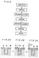
- a preprocess is performed.
- the semiconductor wafer W is immersed in an aqueous sulfuric acid solution to activate the semiconductor wafer W.
- a first plating process is performed by immersing the semiconductor wafer W into a first plating solution, such as a high throwing power copper sulfate plating solution used for printed circuit boards. As shown in Fig. 3A, this process forms a uniform initial plating layer 11 over the surface of a fine pit 10 formed in the semiconductor wafer W, wherein the surface includes the bottom and side walls of the fine pit 10.
- the high throwing power copper sulfate solution has a low concentration of copper sulfate, a high concentration of sulfuric acid, and is superior in throwing power and coating uniformity.
- An example composition of this solution is 5-100 g/l of copper sulfate and 100-250 g/l of sulfuric acid.
- the plating solution has a low concentration of copper sulfate and a high concentration of sulfuric acid, the conductivity of the solution is high and the polarization is great, thereby improving throwing power. As a result, plating metal is uniformly deposited on the surface of the semiconductor wafer W, eliminating unplated areas formed on the side and bottom surfaces of the fine pit 10.
- a second plating process is performed by immersing the semiconductor wafer W into a second plating solution, such as a copper sulfate plating solution for decorative uses.
- a second plating solution such as a copper sulfate plating solution for decorative uses.
- this process forms a plating layer 12 having a flat surface on the surface of the initial plating layer 11.
- the copper sulfate plating solution has a high concentration of copper sulfate and a low concentration of sulfuric acid and is superior in leveling ability.
- An example composition of the solution is 100-300 g/l of copper sulfate and 10-100 g/l of sulfuric acid.
- leveling ability defines a quality describing the degree of smoothness on the plating surface.
- good leveling ability it is possible to obtain a plating layer 15a having a flat surface, as shown in Fig. 4A, even when a depression 14 is formed in the surface of the semiconductor wafer W.
- a plating layer 15b as shown in Fig. 4B, is obtained.
- the shape of the depression 14 formed in the surface of the semiconductor wafer W is reflected in the plating layer 15b.
- film at the inlet to the fine pit 10 grows slow, as shown in Fig. 3B.
- This slow growth can prevent the generation of voids, thereby filling the fine pit 10 with a uniform layer of copper plating having no gaps.
- the semiconductor wafer W is washed and dried to complete the plating process.
- This process achieves a plating layer 13 having a flat surface and free of voids.
- the fine pit 10 contains no unplated areas on its bottom or side walls.
- Fig. 5 shows the construction of a plating apparatus suitable for the plating process described above.
- the plating apparatus is provided with a plating bath 20; a first plating solution supplying section 22a for supplying a first plating solution 21 into the plating bath 20; and a second plating solution supplying section 22b for supplying a second plating solution 23 into the plating bath 20.
- the first plating solution supplying section 22a includes a pump 24a for pumping first plating solution 21 into the plating bath 20; a shut-off valve 25a disposed upstream from the pump 24a; and a timer 26a for opening and closing the shut-off valve 25a.
- the second plating solution supplying section 22b includes a pump 24b for pumping second plating solution 23 into the plating bath 20; a shut-off valve 25b disposed upstream from the pump 24b; and a timer 26b for opening and closing the shut-off valve 25b.
- a wash water supply tube 27 and a discharge tube 28 are connected to the plating bath 20 for introducing wash water into the plating bath 20 and discharging wash water out of the plating bath 20, respectively.
- a pump 29 is connected to the tube 28.
- a semiconductor wafer W having undergone a preprocess is inserted into the plating bath 20. Wash water is introduced into the plating bath 20 and the semiconductor wafer W is washed. Next, the shut-off valve 25a is opened according to the timer 26a. The first plating solution 21 is supplied into the plating bath 20, and the first plating process is performed. After a fixed time has elapsed, the shut-off valve 25a is closed. Wash water is again introduced into the plating bath 20 for washing the semiconductor wafer W. Subsequently, the shut-off valve 25b of the second plating solution supplying section 22b is opened according to timer 26b. The second plating solution 23 is supplied into the plating bath 20 and the second plating process is performed. Accordingly, it is possible to perform both the first and second plating processes consecutively using the same apparatus.
- a timer is used for switching the supply of plating solution on and off.
- any means capable of performing this process can be used.
- the same processing tank is used for performing the first plating process, the second plating process, and the washing processes.
- these processes can be performed using separate baths for each process.
- multiple baths can be provided, wherein the plating process is performed by immersing the semiconductor wafer W into each bath in order according to each step of the process.
- the fine pit 10 having a width of 1.0 ⁇ m or less is formed on the semiconductor wafer W.
- An aqueous solution having 100 g/l of sulfuric acid is maintained at a temperature of 50°C.
- a preprocess is performed by immersing the semiconductor wafer W into the aqueous solution for 15 seconds.
- the first plating process is performed with the first plating solution and, after washing the semiconductor wafer W, the second plating process is performed using the second plating solution.
- the semiconductor wafer W is then washed and dried.
- composition of the first plating solution is as follows. CuSO 4 ⁇ 5H 2 O 70 g/l H 2 SO 4 200 g/l NaCl 100 mg/l Organic additive 5 ml/l
- composition of the second plating solution is as follows. CuSO 4 ⁇ 5H 2 O 200 g/l H 2 SO 4 50 g/l NaCl 100 mg/l Organic additive 5 ml/l
- This process forms the plating layer 13 free of voids in the fine pit 10, as shown in Fig. 6A. No unplated areas are developed in the fine pit 10.
- a semiconductor wafer W having undergone the same preprocess described above is plated using only the first plating solution. As shown in Fig. 6B, a void 30 is formed in the plating layer 13 within the fine pit 10.
- a semiconductor wafer W having undergone the same preprocess described above is plated using only the second plating solution. As shown in Fig. 6C, an unplated area 31 exists in a bottom corner of the fine pit 10.
- a semiconductor wafer W is formed of a semiconductor material 1, a conducting layer 1a formed on the top surface of the semiconductor material 1, and an SiO 2 insulating layer 2 deposited on top of the conducting layer 1a.
- a contact hole 3 and a channel 4 are formed in the insulating layer 2 by a lithography etching technique.
- a preprocess is performed.
- the semiconductor wafer W is immersed in an aqueous sulfuric acid solution to activate the semiconductor wafer W.
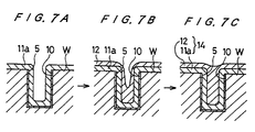
- a first plating process is performed by immersing the semiconductor wafer W into a first plating solution, such as a copper pyrophosphate solution. As shown in Fig. 7A, this process forms a uniform initial plating layer 11 over the surface including the barrier layer 5.
- the barrier layer 5 covers the bottom and side walls of a fine pit 10 formed in the semiconductor wafer W.
- the copper pyrophosphate sulfate solution forms a layered deposition providing superior close adherence with the barrier layer 5.
- this process forms an initial plating layer 11a having a throwing power and prevents the generation of unplated areas on the barrier layer 5 covering the fine pit 10.
- a second plating process is performed by immersing the semiconductor wafer W into a second plating solution, such as a copper sulfate plating solution.
- a second plating solution such as a copper sulfate plating solution.
- this process forms a plating layer 12 having a flat surface on the surface of the initial plating layer 11a.
- the copper sulfate plating solution has a high concentration of copper sulfate and a low concentration of sulfuric acid and is superior in leveling ability.
- An example composition of the solution is 100-300 g/l of copper sulfate and 10-100 g/l of sulfuric acid.
- the fine pit 10 having a width of 1.0 ⁇ m or less is formed on the semiconductor wafer W.
- the barrier layer 5 covers the fine pit 10.
- An aqueous solution having 100 g/l of sulfuric acid is maintained at a temperature of 50°C.
- a preprocess is performed by immersing the semiconductor wafer W into the aqueous solution for 15 seconds.
- the first plating process is performed with the first plating solution and, after washing the semiconductor wafer W, the second plating process is performed using the second plating solution.
- the semiconductor wafer W is then washed and dried.
- composition of the first plating solution is as follows. Cu 2 P 2 O 7 ⁇ 3H 2 O 90 g/l H 4 P 2 O 7 340 g/l Ammonia 3 ml/l Organic additive 0.5 ml/l
- the conditions for the plating process are as follows. Bath temperature 55°C Current density 0.5 A/dm 2 Plating time 3 min. PH 8.5
- composition of the second plating solution is as follows. CuSO 4 ⁇ 5H 2 O 200 g/l H 2 SO 4 50 g/l NaCl 100 mg/l Organic additive 5 ml/l
- the conditions for the plating process are as follows. Bath temperature 25°C Current density 2 A/dm 2 Plating time 2.5 min. PH ⁇ 1
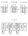
- This process forms a plating layer 14 free of voids in the fine pit 10, as shown in Fig. 8A. No unplated areas are developed on the barrier layer 5 within the fine pit 10.
- a semiconductor wafer W having undergone the same preprocess described above is plated using only the first plating solution. As shown in Fig. 8B, a void 30 is formed in the plating layer 14 within the fine pit 10.
- a semiconductor wafer W having undergone the same preprocess described above is plated using only the second plating solution. As shown in Fig. 8C, an unplated area 31 exists on the barrier layer 5 in a bottom corner of the fine pit 10.
- a uniform initial plating layer without unplated areas on the side walls and bottom of the fine pit 10 is formed.
- a surface plating layer having a smooth surface and no void is formed on top of the initial plating layer. Accordingly, fine pits formed in the substrate, such as fine channels for wiring, can be filled with a copper, copper alloy, or other material having low electrical resistance without gaps in the metal plating and with an level surface.
- the present invention is a plating process capable of forming embedded wiring layers and the like in semiconductor wafers and can be applied to the fabrication of LSI chips and other semiconductor devices.
Landscapes
- Chemical & Material Sciences (AREA)
- Engineering & Computer Science (AREA)
- Materials Engineering (AREA)
- Chemical Kinetics & Catalysis (AREA)
- Electrochemistry (AREA)
- Metallurgy (AREA)
- Organic Chemistry (AREA)
- Microelectronics & Electronic Packaging (AREA)
- Manufacturing & Machinery (AREA)
- Electroplating Methods And Accessories (AREA)
- Electroplating And Plating Baths Therefor (AREA)
- Electrodes Of Semiconductors (AREA)
- Chemically Coating (AREA)
- Internal Circuitry In Semiconductor Integrated Circuit Devices (AREA)
Applications Claiming Priority (5)
| Application Number | Priority Date | Filing Date | Title |
|---|---|---|---|
| JP13615298 | 1998-04-30 | ||
| JP13615298A JP3836252B2 (ja) | 1998-04-30 | 1998-04-30 | 基板のめっき方法 |
| JP13615198 | 1998-04-30 | ||
| JP13615198A JP3904328B2 (ja) | 1998-04-30 | 1998-04-30 | 基板のめっき方法 |
| PCT/JP1999/002271 WO1999057342A1 (en) | 1998-04-30 | 1999-04-28 | Method and device for plating substrate |
Publications (2)
| Publication Number | Publication Date |
|---|---|
| EP1091024A1 true EP1091024A1 (de) | 2001-04-11 |
| EP1091024A4 EP1091024A4 (de) | 2006-03-22 |
Family
ID=26469809
Family Applications (1)
| Application Number | Title | Priority Date | Filing Date |
|---|---|---|---|
| EP99917206A Withdrawn EP1091024A4 (de) | 1998-04-30 | 1999-04-28 | Verfahren und vorrichtung zum beschichten von substraten |
Country Status (5)
| Country | Link |
|---|---|
| US (3) | US6517894B1 (de) |
| EP (1) | EP1091024A4 (de) |
| KR (1) | KR100654413B1 (de) |
| TW (2) | TWI250223B (de) |
| WO (1) | WO1999057342A1 (de) |
Cited By (6)
| Publication number | Priority date | Publication date | Assignee | Title |
|---|---|---|---|---|
| EP1122989A3 (de) * | 2000-02-01 | 2002-07-03 | Shinko Electric Industries Co. Ltd. | Plattierungsverfahren zum Füllen von Kontaktlöchern |
| EP1199384A3 (de) * | 2000-10-20 | 2004-03-03 | Shipley Co. L.L.C. | Plattierungsbad |
| EP1249861A3 (de) * | 2001-03-23 | 2007-11-21 | Interuniversitair Micro-Elektronica Centrum | Ein Mehrschrittverfahren zur Metallabscheidung |
| CN102443830A (zh) * | 2011-10-12 | 2012-05-09 | 上海华力微电子有限公司 | 一种改善电镀铜工艺的方法 |
| EP2692905A3 (de) * | 2012-07-31 | 2016-01-06 | Harry Schaaf | Galvanische Beschichtungsanlage und Verfahren zu deren Betrieb |
| WO2017219797A1 (zh) * | 2016-06-21 | 2017-12-28 | 广东光华科技股份有限公司 | 电镀铜镀液及其电镀铜工艺 |
Families Citing this family (41)
| Publication number | Priority date | Publication date | Assignee | Title |
|---|---|---|---|---|
| US6517894B1 (en) * | 1998-04-30 | 2003-02-11 | Ebara Corporation | Method for plating a first layer on a substrate and a second layer on the first layer |
| US20050006245A1 (en) * | 2003-07-08 | 2005-01-13 | Applied Materials, Inc. | Multiple-step electrodeposition process for direct copper plating on barrier metals |
| US6709563B2 (en) * | 2000-06-30 | 2004-03-23 | Ebara Corporation | Copper-plating liquid, plating method and plating apparatus |
| US20050081744A1 (en) * | 2003-10-16 | 2005-04-21 | Semitool, Inc. | Electroplating compositions and methods for electroplating |
| US6878245B2 (en) * | 2002-02-27 | 2005-04-12 | Applied Materials, Inc. | Method and apparatus for reducing organic depletion during non-processing time periods |
| US20030207206A1 (en) * | 2002-04-22 | 2003-11-06 | General Electric Company | Limited play data storage media and method for limiting access to data thereon |
| JP4555540B2 (ja) * | 2002-07-08 | 2010-10-06 | ルネサスエレクトロニクス株式会社 | 半導体装置 |
| DE10238285A1 (de) * | 2002-08-21 | 2004-03-04 | Siemens Ag | Verfahren und Vorrichtung zum Bereitstellen von Konferenzen |
| JP2004339579A (ja) * | 2003-05-16 | 2004-12-02 | Ebara Corp | 電解処理装置及び方法 |
| JP4344270B2 (ja) * | 2003-05-30 | 2009-10-14 | セイコーエプソン株式会社 | 液晶表示装置の製造方法 |
| US20070125657A1 (en) * | 2003-07-08 | 2007-06-07 | Zhi-Wen Sun | Method of direct plating of copper on a substrate structure |
| US20060283716A1 (en) * | 2003-07-08 | 2006-12-21 | Hooman Hafezi | Method of direct plating of copper on a ruthenium alloy |
| US20050085031A1 (en) * | 2003-10-15 | 2005-04-21 | Applied Materials, Inc. | Heterogeneous activation layers formed by ionic and electroless reactions used for IC interconnect capping layers |
| US20050095830A1 (en) * | 2003-10-17 | 2005-05-05 | Applied Materials, Inc. | Selective self-initiating electroless capping of copper with cobalt-containing alloys |
| US7205233B2 (en) * | 2003-11-07 | 2007-04-17 | Applied Materials, Inc. | Method for forming CoWRe alloys by electroless deposition |
| US20050161338A1 (en) * | 2004-01-26 | 2005-07-28 | Applied Materials, Inc. | Electroless cobalt alloy deposition process |
| US20050170650A1 (en) * | 2004-01-26 | 2005-08-04 | Hongbin Fang | Electroless palladium nitrate activation prior to cobalt-alloy deposition |
| US20060033678A1 (en) * | 2004-01-26 | 2006-02-16 | Applied Materials, Inc. | Integrated electroless deposition system |
| US20060162658A1 (en) * | 2005-01-27 | 2006-07-27 | Applied Materials, Inc. | Ruthenium layer deposition apparatus and method |
| US7438949B2 (en) * | 2005-01-27 | 2008-10-21 | Applied Materials, Inc. | Ruthenium containing layer deposition method |
| US20060240187A1 (en) * | 2005-01-27 | 2006-10-26 | Applied Materials, Inc. | Deposition of an intermediate catalytic layer on a barrier layer for copper metallization |
| WO2006102318A2 (en) * | 2005-03-18 | 2006-09-28 | Applied Materials, Inc. | Electroless deposition process on a contact containing silicon or silicide |
| US7651934B2 (en) | 2005-03-18 | 2010-01-26 | Applied Materials, Inc. | Process for electroless copper deposition |
| US20060251801A1 (en) * | 2005-03-18 | 2006-11-09 | Weidman Timothy W | In-situ silicidation metallization process |
| US20060246699A1 (en) * | 2005-03-18 | 2006-11-02 | Weidman Timothy W | Process for electroless copper deposition on a ruthenium seed |
| US20070071888A1 (en) * | 2005-09-21 | 2007-03-29 | Arulkumar Shanmugasundram | Method and apparatus for forming device features in an integrated electroless deposition system |
| US20070099422A1 (en) * | 2005-10-28 | 2007-05-03 | Kapila Wijekoon | Process for electroless copper deposition |
| US20070099806A1 (en) * | 2005-10-28 | 2007-05-03 | Stewart Michael P | Composition and method for selectively removing native oxide from silicon-containing surfaces |
| US7575666B2 (en) * | 2006-04-05 | 2009-08-18 | James Watkowski | Process for electrolytically plating copper |
| US20100068404A1 (en) * | 2008-09-18 | 2010-03-18 | Guardian Industries Corp. | Draw-off coating apparatus for making coating articles, and/or methods of making coated articles using the same |
| US20120273261A1 (en) | 2010-10-20 | 2012-11-01 | Taiwan Green Point Enterprises Co., Ltd. | Circuit substrate having a circuit pattern and method for making the same |
| US8952919B2 (en) | 2011-02-25 | 2015-02-10 | Taiwan Green Point Enterprises Co., Ltd. | Capacitive touch sensitive housing and method for making the same |
| US8621749B2 (en) | 2010-03-12 | 2014-01-07 | Taiwan Green Point Enterprises Co., Ltd | Non-deleterious technique for creating continuous conductive circuits |
| JP5917297B2 (ja) * | 2012-05-30 | 2016-05-11 | 東京エレクトロン株式会社 | めっき処理方法、めっき処理装置および記憶媒体 |
| CN103547055B (zh) * | 2012-07-10 | 2016-06-08 | 绿点高新科技股份有限公司 | 具有电路图案的电路基板的制造方法 |
| US9758893B2 (en) | 2014-02-07 | 2017-09-12 | Applied Materials, Inc. | Electroplating methods for semiconductor substrates |
| WO2017076456A1 (de) * | 2015-11-05 | 2017-05-11 | Topocrom Systems Ag | Verfahren und vorrichtung zum galvanischen aufbringen einer oberflächenbeschichtung |
| US10352428B2 (en) * | 2016-03-28 | 2019-07-16 | Shimano Inc. | Slide component, bicycle component, bicycle rear sprocket, bicycle front sprocket, bicycle chain, and method of manufacturing slide component |
| US10930511B2 (en) * | 2018-03-30 | 2021-02-23 | Lam Research Corporation | Copper electrodeposition sequence for the filling of cobalt lined features |
| JP7453874B2 (ja) * | 2020-07-30 | 2024-03-21 | 芝浦メカトロニクス株式会社 | 基板処理方法、および基板処理装置 |
| CN118812171A (zh) * | 2023-04-17 | 2024-10-22 | 财团法人工业技术研究院 | 贯穿玻璃的通孔的铜金属化方法和由此制造的玻璃制品 |
Family Cites Families (54)
| Publication number | Priority date | Publication date | Assignee | Title |
|---|---|---|---|---|
| US2438013A (en) * | 1940-07-22 | 1948-03-16 | Patents Corp | Treated steel sheet and process |
| US2546150A (en) * | 1946-11-08 | 1951-03-27 | Brenner Abner | Method for securing adhesion of electroplated coatings to a metal base |
| US2879210A (en) * | 1956-07-02 | 1959-03-24 | Steel Prot And Chemical Compan | Process of electroplating on aluminum |
| DE1928062C3 (de) * | 1968-06-04 | 1974-04-25 | Matsushita Electric Industrial Co., Ltd., Kadoma, Osaka (Japan) | Galvanisierzelle |
| GB1288992A (de) * | 1970-06-22 | 1972-09-13 | ||
| US3716462A (en) | 1970-10-05 | 1973-02-13 | D Jensen | Copper plating on zinc and its alloys |
| US3844909A (en) * | 1970-11-12 | 1974-10-29 | Gen Electric | Magnetic film plated wire and substrates therefor |
| US3930963A (en) | 1971-07-29 | 1976-01-06 | Photocircuits Division Of Kollmorgen Corporation | Method for the production of radiant energy imaged printed circuit boards |
| US3884772A (en) * | 1971-09-25 | 1975-05-20 | Furukawa Electric Co Ltd | Method for producing a heat exchanger element |
| US3753664A (en) * | 1971-11-24 | 1973-08-21 | Gen Motors Corp | Hard iron electroplating of soft substrates and resultant product |
| US3959108A (en) * | 1971-12-27 | 1976-05-25 | Plumpe Jr William H | System for automatically measuring and controlling the sulfate content of a chromium plating solution |
| US3865700A (en) * | 1973-05-18 | 1975-02-11 | Fromson H A | Process and apparatus for continuously anodizing aluminum |
| US3963569A (en) * | 1973-12-06 | 1976-06-15 | Raytheon Company | Apparatus for plating elongated bodies |
| US4039398A (en) * | 1975-08-15 | 1977-08-02 | Daiichi Denshi Kogyo Kabushiki Kaisha | Method and apparatus for electrolytic treatment |
| JPS5817276B2 (ja) * | 1976-10-27 | 1983-04-06 | 古河電気工業株式会社 | 極薄銅箔の製造方法 |
| JPS53143971A (en) * | 1977-05-20 | 1978-12-14 | Hitachi Ltd | Method of producing printed circuit board |
| US4576685A (en) * | 1985-04-23 | 1986-03-18 | Schering Ag | Process and apparatus for plating onto articles |
| JPS62276894A (ja) | 1986-02-21 | 1987-12-01 | 株式会社メイコー | スル−ホ−ル付導体回路板の製造方法 |
| US4959278A (en) | 1988-06-16 | 1990-09-25 | Nippon Mining Co., Ltd. | Tin whisker-free tin or tin alloy plated article and coating technique thereof |
| CA2035970C (en) | 1990-02-09 | 1999-06-01 | Eiji Hirai | Process for surface treating titanium-containing metallic material |
| US5151168A (en) | 1990-09-24 | 1992-09-29 | Micron Technology, Inc. | Process for metallizing integrated circuits with electrolytically-deposited copper |
| JP2832758B2 (ja) * | 1991-02-14 | 1998-12-09 | 日新製鋼株式会社 | 多重巻きパイプ用銅めっき鋼板の製造方法 |
| US5209817A (en) | 1991-08-22 | 1993-05-11 | International Business Machines Corporation | Selective plating method for forming integral via and wiring layers |
| JPH0550775A (ja) * | 1991-08-28 | 1993-03-02 | Toppan Printing Co Ltd | 凹版印刷用基材及びその製造方法 |
| JPH0826475B2 (ja) * | 1991-09-30 | 1996-03-13 | 株式会社神戸製鋼所 | 線条材の銅メッキ方法 |
| JPH0598491A (ja) * | 1991-10-07 | 1993-04-20 | Sumitomo Metal Mining Co Ltd | 電気銅めつき法 |
| JPH05140795A (ja) * | 1991-11-21 | 1993-06-08 | Toagosei Chem Ind Co Ltd | 金属板に支持された電解銅箔の製造方法 |
| CA2082771C (en) * | 1992-11-12 | 1998-02-10 | Vu Quoc Ho | Method for forming interconnect structures for integrated circuits |
| JPH0718485A (ja) * | 1993-07-01 | 1995-01-20 | Furukawa Electric Co Ltd:The | 緑青を形成した材料及びその製造方法 |
| JP2714922B2 (ja) | 1993-07-26 | 1998-02-16 | 東京特殊電線株式会社 | 超極細複合金属めっき線の製造装置 |
| JPH07193214A (ja) | 1993-12-27 | 1995-07-28 | Mitsubishi Electric Corp | バイアホール及びその形成方法 |
| JPH07283219A (ja) * | 1994-04-13 | 1995-10-27 | Sanyo Electric Co Ltd | 半導体装置および半導体装置の製造方法および半導体装 置の製造装置 |
| JPH08126873A (ja) * | 1994-10-28 | 1996-05-21 | Nec Corp | 電子部品等の洗浄方法及び装置 |
| US5625233A (en) | 1995-01-13 | 1997-04-29 | Ibm Corporation | Thin film multi-layer oxygen diffusion barrier consisting of refractory metal, refractory metal aluminide, and aluminum oxide |
| US5750014A (en) * | 1995-02-09 | 1998-05-12 | International Hardcoat, Inc. | Apparatus for selectively coating metal parts |
| US5549808A (en) * | 1995-05-12 | 1996-08-27 | International Business Machines Corporation | Method for forming capped copper electrical interconnects |
| JPH0964044A (ja) * | 1995-08-25 | 1997-03-07 | Toshiba Corp | 半導体装置及びその製造方法 |
| US5913147A (en) | 1997-01-21 | 1999-06-15 | Advanced Micro Devices, Inc. | Method for fabricating copper-aluminum metallization |
| US5933758A (en) * | 1997-05-12 | 1999-08-03 | Motorola, Inc. | Method for preventing electroplating of copper on an exposed surface at the edge exclusion of a semiconductor wafer |
| US5972192A (en) * | 1997-07-23 | 1999-10-26 | Advanced Micro Devices, Inc. | Pulse electroplating copper or copper alloys |
| US5989623A (en) * | 1997-08-19 | 1999-11-23 | Applied Materials, Inc. | Dual damascene metallization |
| TW405158B (en) | 1997-09-17 | 2000-09-11 | Ebara Corp | Plating apparatus for semiconductor wafer processing |
| US5882498A (en) * | 1997-10-16 | 1999-03-16 | Advanced Micro Devices, Inc. | Method for reducing oxidation of electroplating chamber contacts and improving uniform electroplating of a substrate |
| US6020266A (en) * | 1997-12-31 | 2000-02-01 | Intel Corporation | Single step electroplating process for interconnect via fill and metal line patterning |
| US6140234A (en) * | 1998-01-20 | 2000-10-31 | International Business Machines Corporation | Method to selectively fill recesses with conductive metal |
| US7244677B2 (en) | 1998-02-04 | 2007-07-17 | Semitool. Inc. | Method for filling recessed micro-structures with metallization in the production of a microelectronic device |
| JP3523197B2 (ja) * | 1998-02-12 | 2004-04-26 | エーシーエム リサーチ,インコーポレイティド | メッキ設備及び方法 |
| TW593731B (en) | 1998-03-20 | 2004-06-21 | Semitool Inc | Apparatus for applying a metal structure to a workpiece |
| US6197181B1 (en) * | 1998-03-20 | 2001-03-06 | Semitool, Inc. | Apparatus and method for electrolytically depositing a metal on a microelectronic workpiece |
| US5968333A (en) * | 1998-04-07 | 1999-10-19 | Advanced Micro Devices, Inc. | Method of electroplating a copper or copper alloy interconnect |
| US6517894B1 (en) * | 1998-04-30 | 2003-02-11 | Ebara Corporation | Method for plating a first layer on a substrate and a second layer on the first layer |
| US6074544A (en) | 1998-07-22 | 2000-06-13 | Novellus Systems, Inc. | Method of electroplating semiconductor wafer using variable currents and mass transfer to obtain uniform plated layer |
| US6793796B2 (en) * | 1998-10-26 | 2004-09-21 | Novellus Systems, Inc. | Electroplating process for avoiding defects in metal features of integrated circuit devices |
| US6107186A (en) * | 1999-01-27 | 2000-08-22 | Advanced Micro Devices, Inc. | High planarity high-density in-laid metallization patterns by damascene-CMP processing |
-
1999
- 1999-04-28 US US09/674,179 patent/US6517894B1/en not_active Expired - Lifetime
- 1999-04-28 WO PCT/JP1999/002271 patent/WO1999057342A1/ja not_active Ceased
- 1999-04-28 EP EP99917206A patent/EP1091024A4/de not_active Withdrawn
- 1999-04-28 KR KR1020007011820A patent/KR100654413B1/ko not_active Expired - Lifetime
- 1999-04-29 TW TW091111928A patent/TWI250223B/zh active
- 1999-04-29 TW TW088106895A patent/TW530099B/zh active
-
2001
- 2001-12-18 US US10/017,384 patent/US6908534B2/en not_active Expired - Lifetime
-
2004
- 2004-12-10 US US11/008,098 patent/US20050098439A1/en not_active Abandoned
Cited By (7)
| Publication number | Priority date | Publication date | Assignee | Title |
|---|---|---|---|---|
| EP1122989A3 (de) * | 2000-02-01 | 2002-07-03 | Shinko Electric Industries Co. Ltd. | Plattierungsverfahren zum Füllen von Kontaktlöchern |
| US6755957B2 (en) | 2000-02-01 | 2004-06-29 | Shinko Electric Industries Co., Ltd. | Method of plating for filling via holes |
| EP1199384A3 (de) * | 2000-10-20 | 2004-03-03 | Shipley Co. L.L.C. | Plattierungsbad |
| EP1249861A3 (de) * | 2001-03-23 | 2007-11-21 | Interuniversitair Micro-Elektronica Centrum | Ein Mehrschrittverfahren zur Metallabscheidung |
| CN102443830A (zh) * | 2011-10-12 | 2012-05-09 | 上海华力微电子有限公司 | 一种改善电镀铜工艺的方法 |
| EP2692905A3 (de) * | 2012-07-31 | 2016-01-06 | Harry Schaaf | Galvanische Beschichtungsanlage und Verfahren zu deren Betrieb |
| WO2017219797A1 (zh) * | 2016-06-21 | 2017-12-28 | 广东光华科技股份有限公司 | 电镀铜镀液及其电镀铜工艺 |
Also Published As
| Publication number | Publication date |
|---|---|
| TW530099B (en) | 2003-05-01 |
| KR100654413B1 (ko) | 2006-12-05 |
| WO1999057342A1 (en) | 1999-11-11 |
| US20050098439A1 (en) | 2005-05-12 |
| TWI250223B (en) | 2006-03-01 |
| US6908534B2 (en) | 2005-06-21 |
| US20020064591A1 (en) | 2002-05-30 |
| KR20010034825A (ko) | 2001-04-25 |
| US6517894B1 (en) | 2003-02-11 |
| WO1999057342A8 (en) | 2000-01-06 |
| EP1091024A4 (de) | 2006-03-22 |
Similar Documents
| Publication | Publication Date | Title |
|---|---|---|
| US6517894B1 (en) | Method for plating a first layer on a substrate and a second layer on the first layer | |
| US7135098B2 (en) | Copper interconnect seed layer treatment methods and apparatuses for treating the same | |
| US7135404B2 (en) | Method for applying metal features onto barrier layers using electrochemical deposition | |
| KR100420157B1 (ko) | 작업편 상에 전해하여 금속을 증착시키는 장치 및 방법 | |
| US7244677B2 (en) | Method for filling recessed micro-structures with metallization in the production of a microelectronic device | |
| US7115510B2 (en) | Method for electrochemically processing a workpiece | |
| US6943112B2 (en) | Defect-free thin and planar film processing | |
| US7374584B2 (en) | Interconnects forming method and interconnects forming apparatus | |
| US6703712B2 (en) | Microelectronic device layer deposited with multiple electrolytes | |
| JP2003124214A (ja) | 配線形成方法及びその装置 | |
| JP3836252B2 (ja) | 基板のめっき方法 | |
| KR100363847B1 (ko) | 반도체 소자의 금속 배선 형성 방법 | |
| JP3904328B2 (ja) | 基板のめっき方法 | |
| KR100456259B1 (ko) | 반도체 소자의 구리 배선 형성방법 | |
| EP1432016B1 (de) | Herstellung von Kupfer-Verbindungsleitungen mittels Galvanisier-Spül-Galvanisier-Verfahren | |
| JP2006225715A (ja) | めっき装置及びめっき方法 | |
| US7312149B2 (en) | Copper plating of semiconductor devices using single intermediate low power immersion step |
Legal Events
| Date | Code | Title | Description |
|---|---|---|---|
| PUAI | Public reference made under article 153(3) epc to a published international application that has entered the european phase |
Free format text: ORIGINAL CODE: 0009012 |
|
| 17P | Request for examination filed |
Effective date: 20001102 |
|
| AK | Designated contracting states |
Kind code of ref document: A1 Designated state(s): DE FR GB |
|
| D18D | Application deemed to be withdrawn (deleted) | ||
| A4 | Supplementary search report drawn up and despatched |
Effective date: 20060208 |
|
| 17Q | First examination report despatched |
Effective date: 20070509 |
|
| STAA | Information on the status of an ep patent application or granted ep patent |
Free format text: STATUS: THE APPLICATION HAS BEEN WITHDRAWN |
|
| 18W | Application withdrawn |
Effective date: 20101217 |