EP1091202A2 - Capacitive pressure sensor - Google Patents
Capacitive pressure sensor Download PDFInfo
- Publication number
- EP1091202A2 EP1091202A2 EP00250331A EP00250331A EP1091202A2 EP 1091202 A2 EP1091202 A2 EP 1091202A2 EP 00250331 A EP00250331 A EP 00250331A EP 00250331 A EP00250331 A EP 00250331A EP 1091202 A2 EP1091202 A2 EP 1091202A2
- Authority
- EP
- European Patent Office
- Prior art keywords
- recess
- solder
- sub
- sensor according
- pad
- Prior art date
- Legal status (The legal status is an assumption and is not a legal conclusion. Google has not performed a legal analysis and makes no representation as to the accuracy of the status listed.)
- Granted
Links
Images


Classifications
-
- G—PHYSICS
- G01—MEASURING; TESTING
- G01L—MEASURING FORCE, STRESS, TORQUE, WORK, MECHANICAL POWER, MECHANICAL EFFICIENCY, OR FLUID PRESSURE
- G01L9/00—Measuring steady of quasi-steady pressure of fluid or fluent solid material by electric or magnetic pressure-sensitive elements; Transmitting or indicating the displacement of mechanical pressure-sensitive elements, used to measure the steady or quasi-steady pressure of a fluid or fluent solid material, by electric or magnetic means
- G01L9/0041—Transmitting or indicating the displacement of flexible diaphragms
- G01L9/0072—Transmitting or indicating the displacement of flexible diaphragms using variations in capacitance
- G01L9/0075—Transmitting or indicating the displacement of flexible diaphragms using variations in capacitance using a ceramic diaphragm, e.g. alumina, fused quartz, glass
-
- G—PHYSICS
- G01—MEASURING; TESTING
- G01L—MEASURING FORCE, STRESS, TORQUE, WORK, MECHANICAL POWER, MECHANICAL EFFICIENCY, OR FLUID PRESSURE
- G01L9/00—Measuring steady of quasi-steady pressure of fluid or fluent solid material by electric or magnetic pressure-sensitive elements; Transmitting or indicating the displacement of mechanical pressure-sensitive elements, used to measure the steady or quasi-steady pressure of a fluid or fluent solid material, by electric or magnetic means
Definitions
- the present invention relates to a capacitive pressure sensor and, more particularly, to a capacitive pressure sensor in which extraction electrodes made of molten solder are connected to a stationary electrode and movable electrode that constitute a capacitor element.
- a thin wafer constituting a diaphragm and a thick wafer with a recess to form a base are adhered to each other, and the recess and diaphragm constitute a capacitor chamber for a capacitor element. Electrodes constituting the capacitor element are arranged in the capacitor chamber to oppose each other.
- a conventional capacitive pressure sensor 101 is comprised of a lower wafer 102, an upper wafer 103, extraction electrodes 104, a stationary electrode 105, a movable electrode 107, a reference electrode 109, a pad 106 for the stationary electrode 105 and pads 108 for the movable electrode 107 and the reference electrode 109.
- Both the lower and upper wafers 102 and 103 are substrates made of sapphire, silicon, glass, or alumina.
- the lower wafer 102 has a circular recessed capacitor forming portion 102a at its central portion excluding the periphery, and a plurality of pad forming portions 102b and 103b projecting outward from the outer circumference of the capacitor forming portion 102a.
- the upper wafer 103 is bonded to the periphery of the lower wafer 102 so as to cover the capacitor forming portion 102a and pad forming portions 102b and 103b.
- the upper wafer 103 constitutes a diaphragm as it is formed sufficiently thin such that it can be easily deflected in accordance with a change in external pressure.
- the circular movable electrode 107 is fixed in tight contact with the central portion on one surface of the diaphragm opposing the capacitor forming portion 102a, and the C-shaped reference electrode 109 is fixed in tight contact with the edge of the diaphragm to substantially surround the movable electrode 107.
- the circular stationary electrode 105 is fixed in tight contact with the lower wafer 102 to oppose the movable electrode 107 and the reference electrode 109.
- the electrodes 105, 107 and 109 are connected to the extraction electrodes 104 that extend through the lower wafer 102.
- the movable electrode 107 and reference electrode 109 of the upper wafer 103 and the stationary electrode 105 of the lower wafer 102 oppose each other through a predetermined gap to constitute a capacitor element.
- the movable electrode 107 when a diaphragm 103a is deflected by a pressure change, the movable electrode 107 is displaced accordingly to change the distance between the movable electrode 107 and the stationary electrode 105.
- a change in capacitance between the stationary electrode 105 and the movable electrode 107 is electrically detected to measure the pressure change indirectly.
- the reference electrode 109 is used to correct the capacitance detected between the stationary electrode 105 and the movable electrode 107.
- the lower and upper wafers 102 and 103 are prepared by processing a substrate made of sapphire or the like.
- Through holes 110 for forming the extraction electrodes 104 are formed in the lower wafer 102 by machining, a laser process, an ultrasonic process, or the like.
- a recess for the capacitor forming portion 102a is formed in the surface of the lower wafer 102 by dry etching.
- a metal film is formed in the recess by vapor deposition, ion plating, sputtering, or the like, and is selectively etched to form the stationary electrode 105.
- the stationary electrode 105 is formed of a Pt/adhesion promoter film.
- Ti, V, Cr, Nb, Zr, Hf, Ta, or the like is used. Obviously, etching may not be performed and sputtering or the like may be performed through a shadow mask.
- a metal film is formed by sputtering or the like on a substrate made of sapphire or the like, and is selectively etched to form the movable electrode 107, reference electrode 109, and pads 106 and 108.
- the pad 106 is formed of an Au/barrier film/adhesion promoter film.
- Pt is used to form the barrier film
- Nb is used to form the adhesion promoter film.
- sputtering may be performed through a shadow mask to form the electrodes.
- the upper wafer 103 is adhered to the lower wafer 102, and the upper and lower upper wafers 103 and 102 are directly bonded to each other in an atmosphere with a temperature condition of 400°C to 1,300°C.
- molten solder 104a such as Sn-Ag solder is filled in the through holes 110 in the lower wafer 102 to form the extraction electrodes 104. If the lower and upper wafers 102 and 103 are positioned in advance such that the through holes 110 and the pads 106 and 108 oppose each other, the molten solder 104a filled in the through holes 110 attaches to the pads 106 and 108 to make reliable electrical connection.
- the conventional pressure sensor described above has several problems. More specifically, in the upper wafer 103 constituting the diaphragm, the surface where the movable electrode 107 and reference electrode 109 are to be formed and the surface to be bonded to the lower wafer 102 are located on the same plane. If defective electrode formation or wafer misalignment occurs, a misaligned electrode may interfere with bonding the wafers.
- the lower and upper wafers are fabricated from the same material (e.g., sapphire), they are often bonded to each other by direct bonding. Since direct bonding requires planarity and small surface roughness in the bonding surfaces, a misaligned electrode largely decreases the bonding strength of the wafers. For this reason, conventionally, electrodes and lead portions attaching to them must be sufficiently distant from the bonded portions of the wafers. This requires an extra space to interfere with downsizing the sensor.
- the molten solder 104a can flow into the capacitor chamber through interconnections to short-circuit the electrodes with each other.
- a step ⁇ is formed to shorten the distance between the pads 106 and 108 and the openings of the through holes 110, so that the amount of solder that flows out is suppressed.
- a capacitive pressure sensor comprising a first base member with a first main recess and a first sub-recess communicating with the first main recess, a second base member with a second main recess constituting a capacitor chamber together with the first main recess, and a second sub-recess communicating with the second main recess, the second main recess having a bottom surface that constitutes a diaphragm, a stationary electrode formed on a bottom surface of the first main recess, a first pad formed on a bottom surface of the first sub-recess and connected to the stationary electrode through a first interconnection, a movable electrode formed on a bottom surface of the second main recess to oppose the stationary electrode, a second pad formed in the second sub-recess and connected to the movable electrode through a second interconnection, and a plurality of extraction electrodes connected to the first and second pads and extracted outside through through holes formed in the first base
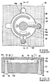
- Figs. 1 and 2 show a capacitive pressure sensor according to the first embodiment of the present invention.
- a capacitive pressure sensor 1 according to this embodiment is comprised of a lower wafer 2, an upper wafer 3, extraction electrodes 4, a stationary electrode 5, a movable electrode 7, a reference electrode 9, two pads 6 for the stationary electrode 5, counter pads 6a opposing the pads 6, pads 8 for the movable electrode 7 and reference electrode 9, and counter pads 8a opposing the pads 8.
- the pads 6 are connected to the stationary electrode 5 through interconnections 5a
- the pads 8 are connected to the movable electrode 7 and reference electrode 9 through interconnections 7a and 9a, respectively.
- Both the lower and upper wafers 2 and 3 are substrates made of sapphire, silicon, glass, or alumina.
- the lower wafer 2 has a circular recessed capacitor forming portion 2a formed at its central portion, and satellite-like small circular recessed pad forming portions 2b communicating with the capacitor forming portion 2a.
- the ring-like pads 6 for the stationary electrode 5 are formed on the bottom surface of the lower wafer 2 constituting the pad forming portions 2b to surround the openings of through holes 10.
- the counter pads 6a are formed on the lower surface of the periphery of the upper wafer 3 to oppose the pads 6.
- the upper wafer 3 has a circular recessed capacitor forming portion 3a formed at its central portion, and a plurality of satellite-like small circular recessed pad forming portions 3b communicating with the capacitor forming portion 3a.
- the pads 8 for the movable electrode 7 and reference electrode 9 are formed on the upper surface of the upper wafer 3 constituting the pad forming portions 3b.
- the ring-like counter pads 8a are formed on the upper surface of the periphery of the lower wafer 2 to surround the openings of the through holes 10 so as to oppose the pads 8.
- the bottom surface of the capacitor forming portion 3a of the upper wafer 3 constitutes a diaphragm as it is formed sufficiently thin such that it can be easily deflected in accordance with a change in external pressure.
- the upper and lower wafers 3 and 2 are bonded to each other at their peripheries so as to seal a capacitor chamber made up from the capacitor forming portions 2a and 3a.
- the capacitor forming portions 2a and 3a do not oppose each other
- the pad forming portions 3a are covered with the upper surface of the periphery of the lower wafer 2
- the pad forming portions 2b are covered with the lower surface of the periphery of the upper wafer 3.
- the circular movable electrode 7 is fixed in tight contact with the central portion of the diaphragm (the bottom surface of the upper wafer 3) constituting the capacitor forming portion 2a, and the C-shaped reference electrode 9 is fixed in tight contact with the edge of the diaphragm so as to substantially surround the movable electrode 7.
- the circular stationary electrode 5 is fixed in tight contact with the lower wafer 2 to oppose the movable electrode 7 and reference electrode 9.
- the electrodes 5, 7, and 9 are connected to the extraction electrodes 4 that extend through the lower wafer 2, as will be described later.
- the capacitor forming portion 3a of the upper wafer 3 and the capacitor forming portion 2a of the lower wafer 2 form the capacitor chamber.
- the movable electrode 7 and reference electrode 9 of the upper wafer 3 and the stationary electrode 5 of the lower wafer 2 oppose each other through a predetermined gap to constitute a capacitor element.
- the movable electrode 7 is displaced accordingly to change the distance between the movable electrode 7 and the stationary electrode 5. Therefore, a change in capacitance between the stationary electrode 5 and the movable electrode 7 is electrically detected to measure the pressure change indirectly.
- the reference electrode 9 is used to correct the capacitance detected between the stationary electrode 5 and the movable electrode 7.
- each pad forming portion 2b has a solder outflow preventive wall 2c to form a bypass for molten solder 4a. More specifically, the pad 6 and counter pad 6a with diameters smaller than that of the pad forming portion 2b are arranged at the central portion of the pad forming portion 2b, formed in the lower wafer 2, to oppose each other.
- the C-shaped solder outflow preventive wall 2c projects from the lower wafer 2 so as to surround the pad 6 and counter pad 6a.
- the solder outflow preventive wall 2c has a notch (opening) on a side opposite to the direction in which the interconnection 5a extends toward the electrode 5.
- Part of the interconnection 5a forms a ring-like shape on the bottom surface (lower wafer 2) of the pad forming portion 2b so as to further surround the solder outflow preventive wall 2c.
- One end of the ring-like shape of the interconnection 5a is connected to the pad 6 through the notch of the solder outflow preventive wall 2c, and the other end is connected to the electrode 5 through the connecting portions of the capacitor forming portion 2a and pad forming portion 2b.
- the molten solder 4a flowing into the portion between the pad 6 and the counter pad 6a through the through hole 10 in the lower wafer 2 flows into the pad forming portion 2b along the ring-like interconnection 5a.
- the molten solder 4a flows along the bypass formed between the solder outflow preventive wall 2c and the wall surface of the pad forming portion 2b inflow of the molten solder 4a into the capacitor forming portion 2a is prohibited.
- the through hole 10 is formed with a taper shape such that its pad forming portion 2b side is narrow, and since the opening at its distal end has a diameter slightly smaller than those of the pads 6 and 6a, inflow of the excessive molten solder 4a to portions other than the pads 6 and 6a is further prohibited.
- the pad forming portions 3b will be described in detail with reference to Figs. 4A and 4B.
- each pad forming portion 3b has a solder outflow preventive wall 3c to form a bypass for the molten solder 4a. More specifically, the pad 8 and the counter pad 8a with diameters smaller than that of the pad forming portion 3b are arranged in the pad forming portion 3b, formed in the upper wafer 3, to oppose each other.
- the C-shaped solder outflow preventive wall 3c projects from the upper wafer 3 so as to surround the pad 8 and the counter pad 8a.
- Part of the interconnection 7a forms a ring-like shape on the bottom surface (upper wafer 3) of the pad forming portion 3b so as to further surround the solder outflow preventive wall 3c.
- One end of the ring-like shape of the interconnection 7a is connected to the pad 8 through the notch of the solder outflow preventive wall 3c, and the other end is connected to the electrode 7 through the connecting portions of the capacitor forming portion 3a and the pad forming portion 3b.
- the molten solder 4a flowing into the portion between the pad 8 and the counter pad 8a through the through hole 10 in the lower wafer 2 flows into the pad forming portion 3b along the interconnection 7a.
- the molten solder 4a flows along the bypass formed between the solder outflow preventive wall 3c and the wall surface of the pad forming portion 3b inflow of the molten solder 4a into the capacitor forming portion 3a is prohibited.
- the through hole 10 is formed with a taper shape such that its pad forming portion 3b side is narrow, and since the opening at its distal end has a diameter slightly smaller than those of the pads 8 and 8a, inflow of the excessive molten solder 4a to portions other than the pads 8 and 8a is further prohibited.
- the pad forming portion 3b corresponding to the electrode 9 and interconnection 9a also has the same structure as this, and a description thereof will accordingly be omitted.
- the lower and upper wafers 2 and 3 are prepared by processing a substrate made of sapphire or the like. More specifically, the through holes 10 for forming the extraction electrodes 4 are formed in the lower wafer 2 by machining, a laser process, an ultrasonic process, or the like. The surface region of the lower wafer 2 is removed by dry etching, and recesses for the capacitor forming portion 2a and the pad forming portions 2b are formed in the lower wafer 2. Metal films are formed on the bottom surfaces of the recesses by vapor deposition, ion plating, sputtering, or the like, and are selectively etched to form the stationary electrode 5, the interconnections 5a and the pads 6. Simultaneously, the counter pads 8a are formed around the lower wafer 2 to correspond to the pad forming portions 3b.
- recesses for the capacitor forming portion 3a and the pad forming portions 3b are formed by dry etching in a substrate made of sapphire or the like. Metal films are formed on the bottom surfaces of the recesses by sputtering or the like, and are etched to form the movable electrode 7, the reference electrode 9, the interconnections 7a and 9a and the pad 8. Simultaneously, the counter pads 6a are formed on the periphery of the upper wafer 3 to correspond to the pad forming portions 2b.
- the electrodes 5, 7, and 9 and the interconnections 5a, 7a, and 9a are formed of Pt/adhesion promoter films.
- Pt/adhesion promoter films For example, Ti, V, Cr, Nb, Zr, Hf, Ta, or the like is used to form the adhesion promoter films.
- the auxiliary pads 6, 8 and 8a are formed of Au/barrier film/adhesion promoter films.
- Pt is used to form barrier films
- Nb is used to form the adhesion promoter films.
- the lower and upper wafers 2 and 3 are adhered to each other, and directly bonded to each other in an atmosphere with a temperature condition of 400°C to 1,300°C.
- the resultant structure is set such that the lower wafer 2 is on the upper side, and the molten solder 4a is filled in the through holes 10, thereby forming the extraction electrodes 4 connected to the pads 6 and 8.
- sputtering may be performed through shadow masks to form the electrodes, interconnections and pads.
- the molten solder 4a can be prevented from attaching to the pads 6 and 6a and 8a and 8a to flow into the capacitor chamber.
- the bypasses formed by the solder preventive walls 2b and 3b prohibit the molten solder 4a from flowing into the capacitor chamber.
- the C-shaped solder outflow preventive wall 2c is formed to have a notch extending in an opposite direction (direction of 180°) to the direction in which the interconnection 5a extends toward the capacitor chamber (electrode 5), thereby forming the bypass for the molten solder 4a.
- outflow of the solder can be prevented more effectively.
- the solder outflow preventive wall 2c is formed with the shape of the question mark, and its one end is connected to the wall surface of the lower wafer 2, so that the length of the bypass can be remarkably increased.
- the notch of the solder outflow preventive wall 2c extends in a direction forming an angle of 90° with the capacitor chamber and the interconnection 5a extends along an arc corresponding to remaining 270°, then the length of the bypass becomes larger than that of the first embodiment by 1.5 times. In this case, it suffices if the direction of the notch of the solder outflow preventive wall 2c forms an angle of 0° to 180° with reference to the extending direction of the interconnection 5a toward the electrode 5.
- the solder outflow preventive projections 10 and 11 are formed at the connecting portions of the pad forming portions 2b and 3b and the capacitor forming portions 2a and 3a, as shown in Fig. 6.
- the solder outflow preventive projection 10 projects from the upper wafer 3, and its distal end comes into contact with the interconnection 5a of the lower wafer 2 to close the outflow path.
- the solder outflow preventive projections 11 project from the lower wafer 2, and their distal ends come into contact with the interconnections 7a and 9a of the upper wafer 3 to close the outflow path.
- solder outflow preventive projections 10 and 11 are formed, even if molten solder 4a flows out from the pad forming portions 2b and 3b, it is reliably prevented from flowing into the capacitor forming portions 2a and 3a.
- solder outflow preventive projections 10 and 11 are formed from a material with poorer solder wettability than that of the interconnections, outflow of the molten solder 4a can be prevented effectively.
- solder outflow preventive projections 10 and 11 disconnect solder flow on only the interconnections 5a, 7, and 9a.
- the solder outflow preventive projections 10 and 11 may disconnect the pad forming portions 2b and 3b and capacitor forming portions 2a and 3a from each other completely.
- solder outflow preventive walls 2c and 3c and solder outflow preventive projections 10 and 11 are formed integrally with the upper or lower wafer 3 or 2.
- separate members may be attached to serve as the solder outflow preventive walls or projections.
- the stationary and movable electrodes are installed in recesses formed in the first and second base members, electrodes do not easily expose to the bonding surfaces of the first and second base members. Therefore, defective bonding of the first and second base members does not occur easily. Unlike in the conventional case, no extra space is required for sufficiently setting apart the bonding portions of the base members and electrode forming portions from each other, thus realizing downsizing the sensor.
- the distance between the openings of the through holes for extraction electrodes and the pads formed on the opposing base member can be decreased, and the molten solder accordingly does not flow out easily.
- the solder outflow preventive walls form the bypass for the molten solder, inflow of the solder into the capacitor chamber is suppressed to prevent short-circuiting of the electrodes.
- solder outflow preventive projections When the solder outflow preventive projections are formed, inflow of the molten solder into the capacitor chamber can be prevented reliably. If the solder outflow preventive projections are made of a material with poorer solder wettability than that of the electrodes, inflow of the solder can be prevented more effectively.
Landscapes
- Physics & Mathematics (AREA)
- General Physics & Mathematics (AREA)
- Chemical & Material Sciences (AREA)
- Engineering & Computer Science (AREA)
- Ceramic Engineering (AREA)
- Measuring Fluid Pressure (AREA)
- Pressure Sensors (AREA)
Abstract
Description
Claims (12)
- A capacitive pressure sensor characterized by comprising:wherein said first and second base members are bonded to each other such that said first and second sub-recesses are covered with bonding surfaces of said second and first base members.a first base member (2) with a first main recess (2a) and a first sub-recess (2b) communicating with said first main recess;a second base member (3) with a second mainrecess (3a) constituting a capacitor chamber together with said first main recess, and a second sub-recess (3b) communicating with said second main recess, said second main recess having a bottom surface that constitutes a diaphragm;a stationary electrode (5) formed on a bottom surface of said first main recess;a first pad (6) formed on a bottom surface of said first sub-recess and connected to said stationary electrode through a first interconnection (5a);a movable electrode (7) formed on a bottom surface of said second main recess to oppose said stationary electrode;a second pad (8) formed in said second sub-recess and connected to said movable electrode through a second interconnection (7a); anda plurality of extraction electrodes (4) connected to said first and second pads and extracted outside through through holes (10) formed in said first base member,
- A sensor according to claim 1, wherein said extraction electrodes are made of molten solder which is filled in said through holes, and is cooled and solidifies to attach to said first and second pads.
- A sensor according to claim 1 or 2, further comprising solder outflow preventive walls (2c) in said first and second sub-recesses to constitute bypasses for the solder flowing out into a portion between said first and second sub-recesses and inner walls thereof.
- A sensor according to claim 3, whereinsaid outflow preventive walls are arranged around said first and second pads in a substantially ring-like shape and have notches forming connection paths for said first and second interconnections to said first and second pads, andsaid first and second interconnections are arranged in a substantially ring-like shape so as to further surround said outflow preventive walls.
- A sensor according to claim 4, wherein said notches of said outflow preventive walls are formed in directions different from directions in which said first and second interconnections extend toward said stationary and movable electrodes.
- A sensor according to claim 4 or 5, wherein said notches of said outflow preventive walls are formed in directions to form angles of substantially 180° with the directions in which said first and second interconnections extend toward said stationary and movable electrodes.
- A sensor according to claim 4 or 5, whereinsaid notches in said outflow preventive walls are formed in directions to form angles of 0° to 180° with the directions in which said first and second interconnections extend toward said stationary and movable electrodes, andsaid first and second interconnections are connected to said stationary and movable electrodes via arcs on sides opposite to the angles formed by said notches of said outflow preventive walls.
- A sensor according to any one of claims 3 to 5, wherein said outflow preventive walls are formed with a C shape.
- A sensor according to any one of claims 3 to 5, wherein said outflow preventive walls are formed with a shape of a question mark, and one end of each of said notches is connected to a corresponding one of said inner walls of said first and second sub-recesses.
- A sensor according to claim 2, further comprising solder outflow preventive members (10, 11) for prohibiting outflow of the molten solder at a communicating portion of said first main recess and said first sub-recess, and a communicating portion of said second main recess and said second sub-recess.
- A sensor according to claim 10, wherein said solder outflow preventive members disconnect outflow paths for the molten solder that flows out on said first and second interconnections from said first and second sub-recesses to said first and second main recesses.
- A sensor according to claim 10, wherein said solder outflow preventive members are made of a material with solder wettability poorer than those of said first and second interconnections.
Applications Claiming Priority (2)
| Application Number | Priority Date | Filing Date | Title |
|---|---|---|---|
| JP28523499 | 1999-10-06 | ||
| JP28523499A JP3588286B2 (en) | 1999-10-06 | 1999-10-06 | Capacitive pressure sensor |
Publications (3)
| Publication Number | Publication Date |
|---|---|
| EP1091202A2 true EP1091202A2 (en) | 2001-04-11 |
| EP1091202A3 EP1091202A3 (en) | 2002-07-10 |
| EP1091202B1 EP1091202B1 (en) | 2004-08-04 |
Family
ID=17688861
Family Applications (1)
| Application Number | Title | Priority Date | Filing Date |
|---|---|---|---|
| EP00250331A Expired - Lifetime EP1091202B1 (en) | 1999-10-06 | 2000-10-05 | Capacitive pressure sensor |
Country Status (6)
| Country | Link |
|---|---|
| US (1) | US6341527B1 (en) |
| EP (1) | EP1091202B1 (en) |
| JP (1) | JP3588286B2 (en) |
| KR (1) | KR100351348B1 (en) |
| CN (1) | CN1125976C (en) |
| DE (1) | DE60012645T2 (en) |
Cited By (4)
| Publication number | Priority date | Publication date | Assignee | Title |
|---|---|---|---|---|
| DE10244077A1 (en) * | 2002-09-06 | 2004-03-11 | INSTITUT FüR MIKROTECHNIK MAINZ GMBH | Production of a semiconductor component used in microelectronics comprises dry etching a hole in the substrate of a component, lining the hole with an insulating layer, removing the insulating layer, and producing an electrical connection |
| EP1851524A4 (en) * | 2005-02-10 | 2011-08-03 | Cardiomems Inc | Hermetic chamber with electrical feedthroughs |
| EP2873958A1 (en) * | 2013-11-15 | 2015-05-20 | Rosemount Aerospace Inc. | Capacitive pressure sensors for high temperature applications |
| CN110031883A (en) * | 2019-03-05 | 2019-07-19 | 中国辐射防护研究院 | One kind being based on wireless condenser type high ionization dose of radiation sensor |
Families Citing this family (24)
| Publication number | Priority date | Publication date | Assignee | Title |
|---|---|---|---|---|
| JP2002350263A (en) * | 2001-05-22 | 2002-12-04 | Kyocera Corp | Package for pressure detector |
| US20060149168A1 (en) * | 2002-08-19 | 2006-07-06 | Robert Czarnek | Capacitive uterine contraction sensor |
| DE102004018408A1 (en) * | 2004-04-16 | 2005-11-03 | Robert Bosch Gmbh | Capacitive pressure sensor and method of manufacture |
| CN1764328B (en) * | 2004-10-18 | 2010-12-15 | 财团法人工业技术研究院 | Dynamic Pressure Sensing Device |
| US7539003B2 (en) * | 2005-12-01 | 2009-05-26 | Lv Sensors, Inc. | Capacitive micro-electro-mechanical sensors with single crystal silicon electrodes |
| JP5092462B2 (en) * | 2006-06-13 | 2012-12-05 | 株式会社デンソー | Mechanical quantity sensor |
| JP4925274B2 (en) * | 2006-08-28 | 2012-04-25 | パナソニック株式会社 | Semiconductor device |
| JP4925275B2 (en) * | 2006-08-28 | 2012-04-25 | パナソニック株式会社 | Semiconductor device |
| JP4925272B2 (en) * | 2006-08-28 | 2012-04-25 | パナソニック株式会社 | Semiconductor device |
| JP4925273B2 (en) * | 2006-08-28 | 2012-04-25 | パナソニック株式会社 | Semiconductor device |
| JP5018261B2 (en) * | 2007-06-14 | 2012-09-05 | 株式会社豊田中央研究所 | Circuit equipment |
| KR101015544B1 (en) * | 2008-03-20 | 2011-02-16 | (주)미코엠에스티 | Capacitive pressure sensor and its manufacturing method |
| US8490495B2 (en) | 2010-05-05 | 2013-07-23 | Consensic, Inc. | Capacitive pressure sensor with vertical electrical feedthroughs and method to make the same |
| CN102183335B (en) | 2011-03-15 | 2015-10-21 | 迈尔森电子(天津)有限公司 | MEMS pressure sensor and preparation method thereof |
| KR101477859B1 (en) * | 2012-05-08 | 2014-12-30 | 한국 한의학 연구원 | Method for manufacturing mems pressure sensor of capacitive type for measuring pulse |
| CN103454018B (en) * | 2012-05-31 | 2015-09-09 | 上海丽恒光微电子科技有限公司 | Pressure transducer, oscillator, ultrasonic sensor and measuring method |
| CN103000699B (en) * | 2012-12-14 | 2015-07-15 | 重庆平伟实业股份有限公司 | Thin high-power and low-forward surface-mounted packaging diode |
| EP2755005A3 (en) | 2013-01-09 | 2017-01-25 | Auto Industrial Co., Ltd. | Output specification calibrating apparatus for capacitive pressure sensor |
| US9837935B2 (en) * | 2013-10-29 | 2017-12-05 | Honeywell International Inc. | All-silicon electrode capacitive transducer on a glass substrate |
| EP3153093B1 (en) | 2014-02-28 | 2019-04-03 | Valencell, Inc. | Method and apparatus for generating assessments using physical activity and biometric parameters |
| CN104931188A (en) * | 2014-03-20 | 2015-09-23 | 立锜科技股份有限公司 | Micro-electromechanical pressure gauge and its manufacturing method |
| DE102016200164B3 (en) * | 2015-10-16 | 2016-03-31 | Ifm Electronic Gmbh | Capacitive pressure measuring cell and pressure gauge with such a pressure measuring cell |
| JP6981885B2 (en) * | 2018-01-23 | 2021-12-17 | アズビル株式会社 | Anomaly detection method and device for capacitive pressure sensor |
| CN115790954A (en) * | 2022-12-27 | 2023-03-14 | 中航光电华亿(沈阳)电子科技有限公司 | Capacitive pressure core |
Family Cites Families (3)
| Publication number | Priority date | Publication date | Assignee | Title |
|---|---|---|---|---|
| EP0339981A3 (en) * | 1988-04-29 | 1991-10-09 | Schlumberger Industries, Inc. | Laminated semiconductor sensor with overpressure protection |
| JPH08254474A (en) * | 1995-03-15 | 1996-10-01 | Omron Corp | Semiconductor type sensor |
| WO1999046570A1 (en) | 1998-03-12 | 1999-09-16 | Yamatake Corporation | Sensor and method of producing the same |
-
1999
- 1999-10-06 JP JP28523499A patent/JP3588286B2/en not_active Expired - Fee Related
-
2000
- 2000-09-30 CN CN00128193A patent/CN1125976C/en not_active Expired - Fee Related
- 2000-10-04 KR KR20000058083A patent/KR100351348B1/en not_active Expired - Fee Related
- 2000-10-04 US US09/680,391 patent/US6341527B1/en not_active Expired - Lifetime
- 2000-10-05 DE DE60012645T patent/DE60012645T2/en not_active Expired - Lifetime
- 2000-10-05 EP EP00250331A patent/EP1091202B1/en not_active Expired - Lifetime
Cited By (7)
| Publication number | Priority date | Publication date | Assignee | Title |
|---|---|---|---|---|
| DE10244077A1 (en) * | 2002-09-06 | 2004-03-11 | INSTITUT FüR MIKROTECHNIK MAINZ GMBH | Production of a semiconductor component used in microelectronics comprises dry etching a hole in the substrate of a component, lining the hole with an insulating layer, removing the insulating layer, and producing an electrical connection |
| DE10244077B4 (en) * | 2002-09-06 | 2007-03-15 | INSTITUT FüR MIKROTECHNIK MAINZ GMBH | Process for the production of semiconductor devices with plated through-hole |
| EP1851524A4 (en) * | 2005-02-10 | 2011-08-03 | Cardiomems Inc | Hermetic chamber with electrical feedthroughs |
| EP2873958A1 (en) * | 2013-11-15 | 2015-05-20 | Rosemount Aerospace Inc. | Capacitive pressure sensors for high temperature applications |
| US9464950B2 (en) | 2013-11-15 | 2016-10-11 | Rosemount Aerospace Inc. | Capacitive pressure sensors for high temperature applications |
| CN110031883A (en) * | 2019-03-05 | 2019-07-19 | 中国辐射防护研究院 | One kind being based on wireless condenser type high ionization dose of radiation sensor |
| CN110031883B (en) * | 2019-03-05 | 2022-06-07 | 中国辐射防护研究院 | High ionizing radiation dose sensor based on wireless capacitance |
Also Published As
| Publication number | Publication date |
|---|---|
| JP3588286B2 (en) | 2004-11-10 |
| JP2001108547A (en) | 2001-04-20 |
| CN1297144A (en) | 2001-05-30 |
| KR100351348B1 (en) | 2002-09-05 |
| EP1091202A3 (en) | 2002-07-10 |
| EP1091202B1 (en) | 2004-08-04 |
| US6341527B1 (en) | 2002-01-29 |
| DE60012645D1 (en) | 2004-09-09 |
| KR20010039983A (en) | 2001-05-15 |
| DE60012645T2 (en) | 2005-08-11 |
| CN1125976C (en) | 2003-10-29 |
Similar Documents
| Publication | Publication Date | Title |
|---|---|---|
| EP1091202B1 (en) | Capacitive pressure sensor | |
| US7530276B2 (en) | Semiconductor pressure sensor and manufacturing method thereof | |
| US5515732A (en) | Capacitive pressure sensor and reference with stress isolating pedestal | |
| US20030116825A1 (en) | Wafer-level package with silicon gasket | |
| CN100397601C (en) | Manufacturing method of semiconductor device and semiconductor device | |
| KR0178624B1 (en) | Semiconductor device having a bump electrode connected to aninner lead | |
| KR20080078784A (en) | Electronic device packages and formation methods | |
| JPH1167820A (en) | Semiconductor device and manufacturing method thereof | |
| JP7408764B2 (en) | MEMS elements and MEMS modules | |
| US7849743B2 (en) | Acceleration sensing device | |
| KR100620810B1 (en) | MEMS device package and manufacturing method thereof | |
| WO2006038395A1 (en) | Electronic apparatus using anodic bonded structure | |
| JP3728969B2 (en) | Capacitance type pressure sensor and manufacturing method thereof | |
| US20090031817A1 (en) | Semiconductor Pressure Sensor and Fabrication Method Thereof | |
| JP2003098026A (en) | Manufacturing method of capacitance type pressure sensor and capacitance type pressure sensor | |
| US6941812B2 (en) | Converter and method of manufacturing the same | |
| JPH02113533A (en) | Semiconductor device | |
| JP3802211B2 (en) | Electrode structure of semiconductor device and method of manufacturing electrode structure in semiconductor device | |
| JPH11186423A (en) | Hermetic seal cover and method of manufacturing the same | |
| KR100273126B1 (en) | Method for fabricating pressure sensor package | |
| KR100270477B1 (en) | Method for fabricating pressure sensor | |
| EP2349915B1 (en) | Electrical contact configuration of micro-electromechanical component and fabrication method | |
| JPH04357881A (en) | Semiconductor pressure sensor wafer and manufacture thereof | |
| KR100210311B1 (en) | Electrode structure and method for anodically-bonded capacitive sensors | |
| JPH0410543A (en) | Formation of bump electrode of semiconductor device |
Legal Events
| Date | Code | Title | Description |
|---|---|---|---|
| PUAI | Public reference made under article 153(3) epc to a published international application that has entered the european phase |
Free format text: ORIGINAL CODE: 0009012 |
|
| AK | Designated contracting states |
Kind code of ref document: A2 Designated state(s): AT BE CH CY DE DK ES FI FR GB GR IE IT LI LU MC NL PT SE |
|
| AX | Request for extension of the european patent |
Free format text: AL;LT;LV;MK;RO;SI |
|
| PUAL | Search report despatched |
Free format text: ORIGINAL CODE: 0009013 |
|
| AK | Designated contracting states |
Kind code of ref document: A3 Designated state(s): AT BE CH CY DE DK ES FI FR GB GR IE IT LI LU MC NL PT SE |
|
| AX | Request for extension of the european patent |
Free format text: AL;LT;LV;MK;RO;SI |
|
| RIC1 | Information provided on ipc code assigned before grant |
Free format text: 7G 01L 9/12 A, 7G 01L 9/00 B |
|
| 17P | Request for examination filed |
Effective date: 20020805 |
|
| AKX | Designation fees paid |
Designated state(s): DE FR GB NL |
|
| GRAP | Despatch of communication of intention to grant a patent |
Free format text: ORIGINAL CODE: EPIDOSNIGR1 |
|
| GRAS | Grant fee paid |
Free format text: ORIGINAL CODE: EPIDOSNIGR3 |
|
| GRAA | (expected) grant |
Free format text: ORIGINAL CODE: 0009210 |
|
| AK | Designated contracting states |
Kind code of ref document: B1 Designated state(s): DE FR GB NL |
|
| PG25 | Lapsed in a contracting state [announced via postgrant information from national office to epo] |
Ref country code: NL Free format text: LAPSE BECAUSE OF FAILURE TO SUBMIT A TRANSLATION OF THE DESCRIPTION OR TO PAY THE FEE WITHIN THE PRESCRIBED TIME-LIMIT Effective date: 20040804 Ref country code: FR Free format text: LAPSE BECAUSE OF FAILURE TO SUBMIT A TRANSLATION OF THE DESCRIPTION OR TO PAY THE FEE WITHIN THE PRESCRIBED TIME-LIMIT Effective date: 20040804 |
|
| REG | Reference to a national code |
Ref country code: GB Ref legal event code: FG4D |
|
| REG | Reference to a national code |
Ref country code: IE Ref legal event code: FG4D |
|
| REF | Corresponds to: |
Ref document number: 60012645 Country of ref document: DE Date of ref document: 20040909 Kind code of ref document: P |
|
| PG25 | Lapsed in a contracting state [announced via postgrant information from national office to epo] |
Ref country code: GB Free format text: LAPSE BECAUSE OF NON-PAYMENT OF DUE FEES Effective date: 20041104 |
|
| NLV1 | Nl: lapsed or annulled due to failure to fulfill the requirements of art. 29p and 29m of the patents act | ||
| PLBE | No opposition filed within time limit |
Free format text: ORIGINAL CODE: 0009261 |
|
| STAA | Information on the status of an ep patent application or granted ep patent |
Free format text: STATUS: NO OPPOSITION FILED WITHIN TIME LIMIT |
|
| GBPC | Gb: european patent ceased through non-payment of renewal fee |
Effective date: 20041104 |
|
| REG | Reference to a national code |
Ref country code: IE Ref legal event code: MM4A |
|
| 26N | No opposition filed |
Effective date: 20050506 |
|
| EN | Fr: translation not filed | ||
| PGFP | Annual fee paid to national office [announced via postgrant information from national office to epo] |
Ref country code: DE Payment date: 20170927 Year of fee payment: 18 |
|
| REG | Reference to a national code |
Ref country code: DE Ref legal event code: R119 Ref document number: 60012645 Country of ref document: DE |
|
| PG25 | Lapsed in a contracting state [announced via postgrant information from national office to epo] |
Ref country code: DE Free format text: LAPSE BECAUSE OF NON-PAYMENT OF DUE FEES Effective date: 20190501 |