EP1091301A2 - Verfahren und Vorrichtung zur Übertragung von Operationspaketen zwischen funktionellen Modulen eines Prozessors - Google Patents
Verfahren und Vorrichtung zur Übertragung von Operationspaketen zwischen funktionellen Modulen eines Prozessors Download PDFInfo
- Publication number
- EP1091301A2 EP1091301A2 EP00308365A EP00308365A EP1091301A2 EP 1091301 A2 EP1091301 A2 EP 1091301A2 EP 00308365 A EP00308365 A EP 00308365A EP 00308365 A EP00308365 A EP 00308365A EP 1091301 A2 EP1091301 A2 EP 1091301A2
- Authority
- EP
- European Patent Office
- Prior art keywords
- packet
- transaction
- request
- response
- packets
- Prior art date
- Legal status (The legal status is an assumption and is not a legal conclusion. Google has not performed a legal analysis and makes no representation as to the accuracy of the status listed.)
- Granted
Links
Images


Classifications
-
- G—PHYSICS
- G06—COMPUTING OR CALCULATING; COUNTING
- G06F—ELECTRIC DIGITAL DATA PROCESSING
- G06F13/00—Interconnection of, or transfer of information or other signals between, memories, input/output devices or central processing units
- G06F13/14—Handling requests for interconnection or transfer
Definitions
- the present invention relates to the transmission of packets which contain transaction attributes.
- the invention is particularly but not exclusively concerned with the transmission of packets in an integrated circuit comprising a plurality of functional modules interconnected via a packet router.
- Request packets define an operation to be performed and response packets indicate that a request has been received and whether or not the operation defined in a request packet has been successfully carried out.
- the integrated circuit processor can comprise a plurality of functional modules connected to a packet router for transmitting and receiving the request and response packets. Transactions involve the dispatch of request packets and receipt of corresponding response packets. Each request packet prompts the generation of an associated response packet which is returned to the indicator of the request.
- control signals which control the arbitration apply globally across the packet router and are generated by the functional modules' internal routing circuitry.
- an integrated circuit comprising: a plurality of functional modules interconnected via a packet router, each functional module having packet handling circuitry for generating and receiving packets conveyed by the packet router; wherein a first set of said functional modules act as initiator modules and have packet handling circuitry which includes request packet generation circuitry for generating request packets for implementing transactions, each request packet including a destination indicator identifying a destination of the packet and a transaction field holding a unique transaction number for each request picket and at least one transaction attribute, and wherein a second set of said functional modules act as target modules and each have packet handling circuitry which includes packet receiver logic for receiving said request packets and response packet generation logic for generating respective response packets, each response packet having a copy of the transaction field transmitted with the respective request packet; the integrated circuit further comprising routing control circuitry which is operable to read said at least one transaction attribute and to control the manner in which packets are conveyed by the packet router responsive to said at least one transaction attribute.
- the unique transaction number uniquely identifies the transaction with which that request packet is associated.
- a response packet is generated which also identifies the unique transaction number. This allows responses and requests to be matched at the initiator module, for example to reorder received responses such that they are properly associated with their respective requests.
- transaction attributes are associated with particular packets rather than with the system control.
- any systems which implement a distributed/hierarchical routing and arbitration system can utilise this information where it is important for system performance, and ignore it at points in the system where it is not. Because the transaction attributes are associated with the packets, they are always available.
- an initiator functional module for connection in an integrated circuit comprising: an interface for supplying and receiving packets to and from the functional module, said interface being connected to a port for connecting the functional module to a packet router; packet handling circuitry for handling said packets and including request packet generating logic which generates request packets for supply to the packet router via the interface, each request packet having a destination indicator identifying a destination of the packet and a transaction field which comprises a unique transaction number for each request packet and at least one transaction attribute for use by routing control of the integrated circuit in routing the transaction over the packet router.
- a further aspect of the invention provides a target functional module for connection in an integrated circuit comprising: an interface for supplying and receiving packets to and from the functional module, said interface being connected to a port for connecting a functional module to a packet router; packet receiver logic which is operable to receive request packets supplied from the packet router via the interface to the target functional module, each request packet having a transaction field including a unique transaction number and at least one transaction attribute, wherein the target module further comprises packet receiver logic for generating respective response packets on receipt of each request packet, each response packet having a transaction field which holds a copy of the unique transaction number and said at least one transaction attribute conveyed by the respective request packet.
- a further aspect of the invention provides a method of implementing transactions in an integrated circuit comprising a plurality of functional modules interconnected via a packet router, the method comprising: at one of said functional modules acting as an initiator module, generating a request packet including a destination indicator identifying a destination of the packet and a transaction field holding a unique transaction number and at least one transaction attribute associated with the transaction; reading the transaction attribute conveyed by the request packet and using the transaction attribute in an arbitration mechanism controlling the flow of packets on the packet router; at the destination indicated by the destination indicator, receiving said request packet and generating a response packet for transmission to the initiator functional module, said response packet holding a copy of the transaction field of the corresponding request packet.
- a further aspect of the invention provides a method of implementing transactions in an integrated circuit comprising a plurality of functional modules interconnected via a packet router, the method comprising: at one of said functional modules acting as an initiator module, generating a request packet including a destination indicator identifying a destination of the packet and a transaction field holding a unique transaction number and a post indicator; detecting the post indicator at a local routing control unit and generating a response packet; at the destination indicated by the destination indicator, receiving said request packet and generating a further response packet with the post indicator set; and detecting receipt of the response packet at the local routing control unit and deleting said packet.
- the transaction field can hold one or a plurality of transaction attributes.
- a first transaction attribute acts as a grouping indicator to indicate to the routing control circuitry that the performance of the system would be enhanced if the packets with this indicator set are kept in an uninterrupted sequence.
- Another transaction attribute acts as a priority indicator to indicate the priority of the transaction.
- the priority indicator can be used at the routing control circuitry to arbitrate transactions on the packet router.
- Another transaction attribute acts as a post bit which, when set in a request packet, causes the routing control circuitry to generate a local response packet.
- a normal response packet with a copy of the transaction field is generated and in this case the routing control circuitry is operable responsive to setting of the post bit in the response packet to locally delete that response packet.
- FIG. 1 illustrates an integrated circuit according to an embodiment of the invention.
- a CPU unit 12 is connected to a plurality of modules M by a data and address path 15 arranged to carry bit packets in parallel form.
- the modules as well as the CPU unit 12 each include packet handling circuitry 2 used in the generation and receipt of bit packets on the path 15.
- the path 15 is referred to herein as a packet router or routing bus.
- Two main types of packet are used on the data and address path 15, each including a destination indicator or address to indicate the required destination module connected to the path 15.
- the packets include request packets which are generated by an initiator module and response packets which are generated by a target module.
- a module may act as both an initiator and a target.
- Response packets are of two types, ordinary responses or error responses. These are discussed in more detail later.
- the modules M as well as the CPU unit 12 each have packet handling circuitry 2 for handling packet formation and receipt of requests, ordinary responses and error responses.
- the routing bus 15 provides bi-directional connections to each module.
- the bus consists of parallel request and response buses and a dedicated control bus provided respectively for each module so as to link the modules to an arbitration unit 22.
- Each module is connected to the routing bus via a port 4 and is provided with an interface 6 incorporating a state machine so as to interchange control signals and data between the port 4 and the interface 6.
- FIG. 1A is a block diagram illustrating relevant functional components of the chip of Figure 1 to illustrate the concept of targets and initiator modules.
- the modules are labelled M1, M2, M3 and M4 and may include any of the modules M already described with reference to Figure 1.
- Modules M1 and M2 both have target and initiator functions as illustrated by the separate target and initiator parts of the interface 6 of each module.
- Module M3 acts only as an initiator and module M4 acts only as a target.
- Signals from the interfaces 6 are supplied to central control logic which forms part of the arbitration unit 22.
- the arbitration unit 22 issues request routing controls and response routing controls to the routing bus network 15.
- the various modules 14 include a debug module 30 which includes an external link 31 for transmitting packets across the chip boundary, an external memory interface EMI 32 having an external bus connection 33 leading to an external memory 50, clock circuitry 34, various peripheral interfaces 35, a peripheral component interface PCI 37 with an external: connection 38, a DMA unit 25 for effecting memory accesses as well as the arbitration unit 22.
- the CPU unit 12 includes a plurality of instruction execution units 40, a plurality of registers 41, and a cache 42.
- the CPU unit 12 also includes packet handling circuitry 2 connected to the execution units 40.
- the routing bus 15 is arranged to transmit to the modules M both request and response packets for effecting memory access transactions as discussed further herein.
- packets may be generated by software as a result of instruction execution by a CPU or by hardware responsive to detection of a packet. Initiator modules can act autonomously to generate packets.
- the packets may be generated on-chip and distributed on the bus 15 or generated off-chip and supplied to the on-chip bus 15 through an external connection such as the link 31 associated with the debug module 30.
- the CPU can be operated in a conventional manner receiving instructions from a program memory and effecting data read or write operations with the cache 42 on-chip. Additionally external memory accesses for read or write operations may be made through the external memory interface 32 and bus connection 33 to the external memory 50.
- the debug module 30 provides an important external communication which may be used for example in debugging procedures.
- the on-chip CPU 12 may obtain instruction code (by memory access packets) for execution from an external source such as a debugging host 60 communicating through the link 31.
- Communications on the routing bus 15 are carried out in bit parallel format. It is possible to reduce the parallelism of packets obtained from the routing bus 15 so that they are output in bit serial format through the link 31.
- Each packet is constructed from one or more cell or token, the end of the packet being identified by an end of packet (eop) signal.
- the construction of the cells is discussed in more detail later.
- each packet cell comprises a number of fields which characterise the packet.
- Each packet is transmitted by a source module and is directed to a destination module.
- An initiator can issue request packets and act on response packets.
- a target can receive and act on requests and issue responses.
- a source module may be an initiator or a target depending on the nature of the packet.
- the source module uses its associated port 4 to transmit a packet onto the routing bus 15.
- the routing bus 15 arranges for the packet to be routed to the port associated with the destination module.
- the destination module then receives that packet from its associated port.
- the source and destination modules can be the same.
- a transaction is an exchange of packets that allows a module to access the state of another module.
- a transaction consists of the transfer of a request packet from a source module to a destination module, followed by the transfer of a response packet from that destination module (now acting as a responding module) back to the source module which made the original request.
- the request packet initiates a transaction and its contents determine the access to be made.
- the response packet completes the transaction and its contents indicate the result of the access.
- a response packet also indicates whether the request was valid or not. If the request was valid, a so-called ordinary response packet is sent. If the request was invalid, an error response packet is transmitted.
- the packet handler 2 comprises request generator logic 200, ordinary response generator logic 202, error response generator logic 204, request packet receiver logic 206, and response packet receiver logic 208. These are all under the general functional control of a control logic block 210.
- a request packet is constructed by a requesting module when that module needs to make an access to a particular target module.
- the address of the target module is recorded in the request packet destination field.
- the requesting module acts as a source of the request packet and sends that packet into the routing bus 15.
- the routing bus 15 arranges for that request packet to be routed from its source to its destination.
- the destination receives the request packet from the routing bus 15.
- the request packet receiver logic 206 checks whether or not the request is valid at 206a. If it is valid, an ordinary response packet is generated by the ordinary response generator logic 202 and the module services the requested access according to the information in the received request packet. If the request is not valid, the error response generator logic 204 generates an error response packet.
- a response packet (ordinary or error) is constructed in order to reply to the request packet.
- the module which originated the request packet is recorded in the response packet's destination field.
- the responding module is the source of the response packet and sends that packet onto the routing bus 15. This is done by the module interface 6.
- the response receiver logic 208 receives the response packet from the routing bus 15 and checks the response at 208a. If the response can be matched to the original request, the transaction is completed.
- Figure 3 shows the information carried by each request cell.
- Each packet is constructed from a series of cells framed using an end of packet (eop) signal.
- Each request cell comprises a 32-bit address field which indicates the destination address of the packet.
- an address comprises an 8-bit destination field 73 followed by a 24-bit offset field 63 which identifies a memory location within the destination. The offset information is present in request packets to identify the particular memory location at which the request is targeted.
- the destination field 73 is a 1-byte field used to route the packet to the destination or target module.
- a byte 74 conveys the opcode which identifies the nature of the requested access.
- the opcode can define a load word access for reading a register value and a store word access for writing a register value.
- a SRC byte 99 is a source field which identifies the source module and which is used as a return address for a response packet.
- a transaction field byte 98 conveys a unique transaction number which is used by the requester to associate responses with requests. The transaction number enables a module to identify response packets corresponding to respective request packets in cases where a plurality of request packets have been sent before response packets have been received for each request packet. As discussed in more detail later, the transaction field also holds transaction attributes describing the transaction to the system.
- a 64-bit data field 71 holds data to be conveyed with the request.
- Figure 4 illustrates the construction of a response packet cell. If the response packet contains more information than a single cell, it is constructed from a sequence of cells framed using a response end of packet (r_eop) signal.
- the response packet includes an opcode byte 85 which denotes the nature of the requested transaction, a byte 84 which identifies the source module of the requesting packet which gave rise to the response and which acts as the return address for the response packet, a transaction field byte 98 and a data field 69.
- the transaction field byte of a response packet holds a copy of the transaction field byte 98 of the corresponding request packet.
- the opcode field 74 of a request packet has a number of different possible encodings to define the nature of the requested access. Bit 7 of the opcode is used to identify whether it is a request or a response packet however. With bit 7 set to one, the packet is a response and which bit 7 set to zero, the packet is a request. The opcode field 85 of the response packet thus has bit 7 set to one in each case. In addition, bit 0 is set to zero if the response is a ordinary response (successful transaction), and is set to one if it is an error response. Thus, the opcode field can quickly and readily identify whether a packet is a request or a response and whether the response is an ordinary response or an error response.
- the function of the arbitration unit is to control packet flow on the packet router.
- the system guarantees to start all operations from a single source to a single memory location in the same order, to route all responses from a single source back to the same initiator and, in an order system, to return all responses back to a single source in the same order as requests were issued.
- the basic function of the arbitration unit follows below. It will readily be appreciated however that any suitable arbitration mechanism can be utilised with the transaction attributes discussed herein.
- a module When a module has a packet to send to another module, for example from the CPU unit 12 to the EMI module 32, it first signals this by asserting a request signal req to a dedicated line connecting that module to the central arbitration unit 22.
- M1 is the initiator module and M2 the target module. It also outputs an eight bit signal to indicate to the arbitration unit 22 the intended destination of the packet it wishes to transmit.
- a module M which is able to receive a packet from the routing bus 15 will assert a grant signal gnt to the central arbitration unit 22 regardless of whether a packet is available to be fed to that destination or not.
- the central arbitration unit 22 determines that a module wishes to send a packet to a destination and independently the destination has indicated that it is able to receive a packet from the bus 15, the unit 22 arranges for the transfer to take place.
- the unit 22 asserts a "grant send" signal gnt_snd to the appropriate interface 6 causing the sending module to put the packet onto the bus 15.
- the arbitration unit 22 then asserts a "send” signal snd which signals to the receiving module that it should accept the transfers currently on the bus 15.
- the packet transmission concludes when the sender asserts an "end of packet" signal concurrently with the last transfer of packet data on the bus 15.
- Figure 5 also illustrates signals derived from the transaction attributes which are used in routing control and arbitration. These are discussed later.
- IM denotes an initiator module
- TM denote a target module
- PR denotes the packet router or routing bus 15.
- a transaction is initiated by forming a request packet at the initiator module.
- the request packet is placed onto the packet router 15 by the initiator port associated with the initiator module IM and is conveyed by the packet router 15 to the target module defined in the destination field of the request packet.
- the memory access operation requested in the request packet is implemented and a response packet is formulated by the target module, placed on the packet router via the port associated with the target module and returned to the initiator module. Only then is a transaction deemed to be completed.
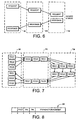
- Figure 6 illustrates a so-called primitive transaction made up of a single request and response.
- Each request packet carries a unique transaction indicator which identifies that transaction by a number generated by the initiator module. This will be termed herein the transaction number.
- the response packet When the response packet is formulated at the target module TM, it contains the same transaction number as that conveyed by the request packet. Thus, when the response packet is received at the initiator module, the transaction number conveyed by the response can be matched to the transaction number of the initial request to confirm that the transaction has been completed.
- Each request packet generated by a particular initiator module has a unique transaction number.
- a compound transaction involves multiple request/response packets from a single module. This is illustrated diagrammatically in Figure 7. It is assumed for the purposes of the example of Figure 7 that this particular compound transaction involves the issuance of three request packet REQ1, REQ2, REQ3 by the initiator module. These request packets are transmitted via the packet router 15 to the target module. By using the lock signal described later, the arbitration module 22 controls the packet flow across the packet router to ensure that all three request packets are conveyed from the initiator module to the target module without interruption. As each request packet reaches the target module, a respective response packet REP1, REP2, REP3 is generated and conveyed by the packet router 15 to the initiator module.
- Each of the request packets REQ1, REQ2, REQ3 in the same compound transaction shares the same transaction number which is returned in the associated response packets.
- the fact that the transaction is a compound transaction can be conveyed in the opcode of the request packets.
- the arbitration unit 22 is caused to ensure that the initiator module remains locked until the complete compound transaction has been finished.
- TMI transaction message information
- Another form of transaction is a so-called linked or grouped transaction.
- a TMI transaction message information
- a TMI (transaction message information) bit in the transaction identifier field indicates that performance of the system may be enhanced if packets in which this attribute is set are treated preferentially by the arbitration unit 22. For example, in the case of a round-robin arbiter which rotates after each access, it could indicate to the arbitration unit that the next member packet in the linked group should be allowed access to the packet router.
- the TMI bit is set to zero, this indicates that the transaction has no relationship with the next transaction (end of message) or, when the bit is set to one, it indicates that the next transaction is related to this transaction (part of a message).
- the packet protocol described herein allows for the existence of this TMI bit which may be utilised by the arbitration unit 22 as described to enforce the grouping as the system performance requirements demand it. However, if the system performance does not require it, the bit can simply be ignored without impacting the arbitration performance.
- a good example of use of the TMI bit is where a plurality of accesses are to be made to the same page in memory via the EMI interface 32. By linking these accesses, the EMI interface can more efficiently utilise its resources to access the page rather than treating each access as a new access.
- the TMI bit is included in both the request and response packets and therefore may be used to enhance the transaction performance of one or both phases.
- Figure 8 is a diagram illustrating the bit encoding of the transaction identification field 98 illustrated in Figures 3 and 4. Note that the same enhancements are available in both the request and response packets. It is the same in both request and response packets.
- a response packet contains a copy of the request packet transaction field.
- the transaction identifier field includes a priority bit PRI and a post bit POST. The function of these bits will be described later with reference to the routing control mechanism.
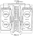
- Figure 9 illustrates the signals which are supplied between the interfaces of respective initiator and target modules and their associated ports 4.
- each line conveyed between the interface 6 and its respective port 4 is marked with a signal name.
- These signal names are used in the following to denote the signals carried by appropriate wires, without reference numerals for the sake of clarity of the diagram of Figure 9.
- the same signal names are used in Figure 5.
- Some of the signals are generated by control logic in the module, while other signals are generated from fields in the packets which are formed by the packet handling circuitry of each module.
- the initiator module includes control logic 210, request generator logic 200 and response receiver logic 208.
- the target module also includes control logic 210 and further includes request receiver logic 206 and a response generator which is labelled 202,204.
- the ordinary response generator logic and the error response generator logic illustrated in Figure 2 have been combined into one block for the purposes of explanation of Figure 9.
- control logic 210 In the initiator module, the control logic 210 generates request req and end of packet eop signals.
- the request generator logic formulates a request packet as described earlier which causes the following signals to be generated:
- the initiator module receives the following signals.
- a response end of packet signal r_eop is received by the control logic 210 as is the grant signal gnt.
- the response receiver logic 208 receives the following response packet signals r_opc, r_data, r_src, r_tid, r_pri and r_lck.
- the grant signal gnt, the response end of packet signal r_eop are generated by the control block 210.
- the remaining signals are formulated from the packet which is generated by the response generator.
- the dest, request, grant, end of packet, lock and priority signals on both the request and response sides are utilised by the arbitration unit 22 to control packet flow.
- the remaining signals are not required for arbitration and are therefore routed directly from an initiator module to the destination target module.
- the transaction field 98 contains information of both kinds.
- the transaction number uniquely identifies a transaction to allow request and response packets to be matched at the initiator module.
- the transaction number is copied from a request packet to a response packet for this purpose.
- the TMI bit of a transaction field can be used to advise the arbitration unit that performance will be improved if all of the request packets in a linked group can be transmitted in uninterrupted fashion across the routing bus 15.
- the TMI bit in a request packet is copied into the respective response packet so that the responses can be similarly treated.
- the priority bit PRI likewise is derived from the transaction field and is used to control the priority with which the particular transaction is routed. Once again, the priority bit is copied from the transaction field of the request packet into the transaction field of the response packet.
- the transaction field 98 also includes a post bit POST which is used by routing control which may be present in the arbitration unit 22 or elsewhere in the system to create a local response packet when a request packet having the post bit set is received.
- POST post bit
- routing control which may be present in the arbitration unit 22 or elsewhere in the system to create a local response packet when a request packet having the post bit set is received.
- Valid sizes for m are defined to be 2 n were n is an integer in the range 0-6.
- Valid sizes for m are defined to be 2 n where n is an integer in the range 0-6.
- Valid sizes for m are defined to be 2 n where n is an integer in the range 0-6.
- Valid sizes for m are defined to be 2 n where n is an integer in the range 0-6.
- Load a Group of words of M bytes Load Group
- the group consists of a number of elements, each of which contains m bytes, valid values for m are 2 n where n is an integer in the range 0-6.
- the group contains g* m bytes of data, and is complete when eop is asserted on the final cell of the final word to be transferred.
- the operation is a mechanism for the initiator to force the system to maintain a series of possibly unrelated operations as a single element.
- the group consists of a number of elements, each of which contains m bytes, valid values for m are 2 n where n is an integer in the range 0-6.
- the group contains g* m bytes of data, and is complete when eop is asserted on the final cell of the final word to be transferred.
- This operation is a mechanism for the initiator to force the system to maintain a series of possibly unrelated operations as a single element.
Landscapes
- Engineering & Computer Science (AREA)
- Theoretical Computer Science (AREA)
- Physics & Mathematics (AREA)
- General Engineering & Computer Science (AREA)
- General Physics & Mathematics (AREA)
- Data Exchanges In Wide-Area Networks (AREA)
Applications Claiming Priority (2)
| Application Number | Priority Date | Filing Date | Title |
|---|---|---|---|
| US411419 | 1999-10-01 | ||
| US09/411,419 US6826191B1 (en) | 1999-10-01 | 1999-10-01 | Packets containing transaction attributes |
Publications (3)
| Publication Number | Publication Date |
|---|---|
| EP1091301A2 true EP1091301A2 (de) | 2001-04-11 |
| EP1091301A3 EP1091301A3 (de) | 2004-07-28 |
| EP1091301B1 EP1091301B1 (de) | 2006-04-19 |
Family
ID=23628847
Family Applications (1)
| Application Number | Title | Priority Date | Filing Date |
|---|---|---|---|
| EP00308365A Expired - Lifetime EP1091301B1 (de) | 1999-10-01 | 2000-09-25 | Verfahren und Vorrichtung zur Übertragung von Operationspaketen zwischen funktionellen Modulen eines Prozessors |
Country Status (3)
| Country | Link |
|---|---|
| US (1) | US6826191B1 (de) |
| EP (1) | EP1091301B1 (de) |
| DE (1) | DE60027379D1 (de) |
Cited By (3)
| Publication number | Priority date | Publication date | Assignee | Title |
|---|---|---|---|---|
| WO2005038659A1 (en) * | 2003-10-03 | 2005-04-28 | Sonics, Inc. | Low power shared link arbitration |
| US7149829B2 (en) | 2003-04-18 | 2006-12-12 | Sonics, Inc. | Various methods and apparatuses for arbitration among blocks of functionality |
| US7739436B2 (en) | 2004-11-01 | 2010-06-15 | Sonics, Inc. | Method and apparatus for round robin resource arbitration with a fast request to grant response |
Families Citing this family (10)
| Publication number | Priority date | Publication date | Assignee | Title |
|---|---|---|---|---|
| US7072817B1 (en) | 1999-10-01 | 2006-07-04 | Stmicroelectronics Ltd. | Method of designing an initiator in an integrated circuit |
| US7117301B1 (en) * | 2001-12-27 | 2006-10-03 | Netlogic Microsystems, Inc. | Packet based communication for content addressable memory (CAM) devices and systems |
| US7301961B1 (en) | 2001-12-27 | 2007-11-27 | Cypress Semiconductor Corportion | Method and apparatus for configuring signal lines according to idle codes |
| US7024492B2 (en) * | 2002-05-24 | 2006-04-04 | Convedia Corporation | Media bus interface arbitration for a data server |
| US8016192B2 (en) * | 2006-06-06 | 2011-09-13 | Motorola Mobility, Inc. | User-configurable priority list for mobile device electronic payment applications |
| JP2009032857A (ja) * | 2007-07-26 | 2009-02-12 | Hitachi Ltd | 半導体集積回路および半導体装置 |
| US8897134B2 (en) * | 2010-06-25 | 2014-11-25 | Telefonaktiebolaget L M Ericsson (Publ) | Notifying a controller of a change to a packet forwarding configuration of a network element over a communication channel |
| US9471538B2 (en) | 2012-09-25 | 2016-10-18 | Qualcomm Technologies, Inc. | Network on a chip socket protocol |
| KR101690568B1 (ko) * | 2012-09-25 | 2016-12-28 | 퀄컴 테크놀로지스, 인크. | 네트워크 온 칩 소켓 프로토콜 |
| CN114826819B (zh) * | 2022-06-30 | 2022-11-18 | 深圳核心医疗科技有限公司 | 信息传输方法、装置、设备和存储介质 |
Family Cites Families (77)
| Publication number | Priority date | Publication date | Assignee | Title |
|---|---|---|---|---|
| EP0165600B1 (de) | 1984-06-20 | 1991-11-21 | Convex Computer Corporation | Ein-/Ausgabebus für Rechner |
| US4719621A (en) * | 1985-07-15 | 1988-01-12 | Raytheon Company | Packet fastbus |
| US4935867A (en) | 1986-03-04 | 1990-06-19 | Advanced Micro Devices, Inc. | Signal processor memory management unit with indirect addressing using selectable offsets and modulo values for indexed address calculations |
| US4814981A (en) | 1986-09-18 | 1989-03-21 | Digital Equipment Corporation | Cache invalidate protocol for digital data processing system |
| US5483518A (en) | 1992-06-17 | 1996-01-09 | Texas Instruments Incorporated | Addressable shadow port and protocol for serial bus networks |
| JPH0666056B2 (ja) | 1989-10-12 | 1994-08-24 | 甲府日本電気株式会社 | 情報処理システム |
| JPH03217949A (ja) | 1990-01-23 | 1991-09-25 | Hitachi Ltd | 計算機システム |
| US5452432A (en) | 1990-08-14 | 1995-09-19 | Chips And Technologies, Inc. | Partially resettable, segmented DMA counter |
| JP2984463B2 (ja) | 1991-06-24 | 1999-11-29 | 株式会社日立製作所 | マイクロコンピュータ |
| US5423050A (en) | 1991-11-27 | 1995-06-06 | Ncr Corporation | Intermodule test across system bus utilizing serial test bus |
| US5724549A (en) | 1992-04-06 | 1998-03-03 | Cyrix Corporation | Cache coherency without bus master arbitration signals |
| GB2266606B (en) | 1992-04-27 | 1996-02-14 | Intel Corp | A microprocessor with an external command mode |
| US5448576A (en) | 1992-10-29 | 1995-09-05 | Bull Hn Information Systems Inc. | Boundary scan architecture extension |
| JPH06150023A (ja) | 1992-11-06 | 1994-05-31 | Hitachi Ltd | マイクロコンピュータ及びマイクロコンピュータシステム |
| JP3524110B2 (ja) | 1992-11-06 | 2004-05-10 | 株式会社ルネサステクノロジ | マイクロコンピュータシステム |
| JP3231429B2 (ja) | 1992-11-06 | 2001-11-19 | 株式会社日立製作所 | 中央処理装置と乗算器とを有する半導体集積回路装置 |
| JP3451103B2 (ja) * | 1992-11-27 | 2003-09-29 | 富士通株式会社 | データ通信装置及び方法 |
| US5627842A (en) | 1993-01-21 | 1997-05-06 | Digital Equipment Corporation | Architecture for system-wide standardized intra-module and inter-module fault testing |
| JP2731692B2 (ja) | 1993-04-28 | 1998-03-25 | 日本電気アイシーマイコンシステム株式会社 | デバッグ装置 |
| US5598551A (en) | 1993-07-16 | 1997-01-28 | Unisys Corporation | Cache invalidation sequence system utilizing odd and even invalidation queues with shorter invalidation cycles |
| EP0636976B1 (de) | 1993-07-28 | 1998-12-30 | Koninklijke Philips Electronics N.V. | Mikrokontroller mit hardwaremässiger Fehlerbeseitigungsunterstützung nach dem Boundary-Scanverfahren |
| JP3904244B2 (ja) | 1993-09-17 | 2007-04-11 | 株式会社ルネサステクノロジ | シングル・チップ・データ処理装置 |
| EP0652516A1 (de) | 1993-11-03 | 1995-05-10 | Advanced Micro Devices, Inc. | Integrierter Mikroprozessor |
| US5596734A (en) | 1993-12-17 | 1997-01-21 | Intel Corporation | Method and apparatus for programming embedded memories of a variety of integrated circuits using the IEEE test access port |
| US5828825A (en) | 1993-12-22 | 1998-10-27 | Intel Corporation | Method and apparatus for pseudo-direct access to embedded memories of a micro-controller integrated circuit via the IEEE test access port |
| US5434804A (en) | 1993-12-29 | 1995-07-18 | Intel Corporation | Method and apparatus for synchronizing a JTAG test control signal to an on-chip clock signal |
| US5488688A (en) | 1994-03-30 | 1996-01-30 | Motorola, Inc. | Data processor with real-time diagnostic capability |
| JPH07287668A (ja) | 1994-04-19 | 1995-10-31 | Hitachi Ltd | データ処理装置 |
| GB9417602D0 (en) | 1994-09-01 | 1994-10-19 | Inmos Ltd | A controller for implementing scan testing |
| JPH08329687A (ja) | 1995-06-05 | 1996-12-13 | Hitachi Ltd | 半導体集積回路 |
| JP3672634B2 (ja) | 1994-09-09 | 2005-07-20 | 株式会社ルネサステクノロジ | データ処理装置 |
| JP3713312B2 (ja) | 1994-09-09 | 2005-11-09 | 株式会社ルネサステクノロジ | データ処理装置 |
| JP3740195B2 (ja) | 1994-09-09 | 2006-02-01 | 株式会社ルネサステクノロジ | データ処理装置 |
| US5848247A (en) | 1994-09-13 | 1998-12-08 | Hitachi, Ltd. | Microprocessor having PC card interface |
| US5613153A (en) | 1994-10-03 | 1997-03-18 | International Business Machines Corporation | Coherency and synchronization mechanisms for I/O channel controllers in a data processing system |
| US5751621A (en) | 1994-11-17 | 1998-05-12 | Hitachi, Ltd. | Multiply-add unit and data processing apparatus using it |
| TW330265B (en) | 1994-11-22 | 1998-04-21 | Hitachi Ltd | Semiconductor apparatus |
| JP2752592B2 (ja) | 1994-12-28 | 1998-05-18 | 日本ヒューレット・パッカード株式会社 | マイクロプロセッサ、マイクロプロセッサ−デバッグツール間信号伝送方法及びトレース方法 |
| US5778237A (en) | 1995-01-10 | 1998-07-07 | Hitachi, Ltd. | Data processor and single-chip microcomputer with changing clock frequency and operating voltage |
| US5664197A (en) | 1995-04-21 | 1997-09-02 | Intel Corporation | Method and apparatus for handling bus master channel and direct memory access (DMA) channel access requests at an I/O controller |
| US5867726A (en) | 1995-05-02 | 1999-02-02 | Hitachi, Ltd. | Microcomputer |
| US5570375A (en) | 1995-05-10 | 1996-10-29 | National Science Council Of R.O.C. | IEEE Std. 1149.1 boundary scan circuit capable of built-in self-testing |
| US5860127A (en) | 1995-06-01 | 1999-01-12 | Hitachi, Ltd. | Cache memory employing dynamically controlled data array start timing and a microcomputer using the same |
| US5774701A (en) | 1995-07-10 | 1998-06-30 | Hitachi, Ltd. | Microprocessor operating at high and low clok frequencies |
| US5708773A (en) | 1995-07-20 | 1998-01-13 | Unisys Corporation | JTAG interface system for communicating with compliant and non-compliant JTAG devices |
| US5704034A (en) | 1995-08-30 | 1997-12-30 | Motorola, Inc. | Method and circuit for initializing a data processing system |
| US5737516A (en) | 1995-08-30 | 1998-04-07 | Motorola, Inc. | Data processing system for performing a debug function and method therefor |
| JP3655403B2 (ja) | 1995-10-09 | 2005-06-02 | 株式会社ルネサステクノロジ | データ処理装置 |
| JP3623840B2 (ja) | 1996-01-31 | 2005-02-23 | 株式会社ルネサステクノロジ | データ処理装置及びマイクロプロセッサ |
| US5950012A (en) | 1996-03-08 | 1999-09-07 | Texas Instruments Incorporated | Single chip microprocessor circuits, systems, and methods for self-loading patch micro-operation codes and patch microinstruction codes |
| US5978874A (en) | 1996-07-01 | 1999-11-02 | Sun Microsystems, Inc. | Implementing snooping on a split-transaction computer system bus |
| JPH09311786A (ja) | 1996-03-18 | 1997-12-02 | Hitachi Ltd | データ処理装置 |
| JP3579205B2 (ja) | 1996-08-06 | 2004-10-20 | 株式会社ルネサステクノロジ | 半導体記憶装置、半導体装置、データ処理装置及びコンピュータシステム |
| GB9617033D0 (en) | 1996-08-14 | 1996-09-25 | Int Computers Ltd | Diagnostic memory access |
| US5768152A (en) | 1996-08-28 | 1998-06-16 | International Business Machines Corp. | Performance monitoring through JTAG 1149.1 interface |
| JP3778573B2 (ja) | 1996-09-27 | 2006-05-24 | 株式会社ルネサステクノロジ | データプロセッサ及びデータ処理システム |
| JP3790307B2 (ja) | 1996-10-16 | 2006-06-28 | 株式会社ルネサステクノロジ | データプロセッサ及びデータ処理システム |
| JPH10177520A (ja) | 1996-10-16 | 1998-06-30 | Hitachi Ltd | データプロセッサ及びデータ処理システム |
| JP3641327B2 (ja) | 1996-10-18 | 2005-04-20 | 株式会社ルネサステクノロジ | データプロセッサ及びデータ処理システム |
| EP0840221B1 (de) | 1996-10-31 | 2002-09-18 | STMicroelectronics Limited | Mikrorechner mit Paketbus |
| GB9622686D0 (en) | 1996-10-31 | 1997-01-08 | Sgs Thomson Microelectronics | A test port controller and a method of effecting communication using the same |
| US5983017A (en) | 1996-11-12 | 1999-11-09 | Lsi Logic Corporation | Virtual monitor debugging method and apparatus |
| US5953538A (en) | 1996-11-12 | 1999-09-14 | Digital Equipment Corporation | Method and apparatus providing DMA transfers between devices coupled to different host bus bridges |
| US5771240A (en) | 1996-11-14 | 1998-06-23 | Hewlett-Packard Company | Test systems for obtaining a sample-on-the-fly event trace for an integrated circuit with an integrated debug trigger apparatus and an external pulse pin |
| US5956477A (en) | 1996-11-25 | 1999-09-21 | Hewlett-Packard Company | Method for processing information in a microprocessor to facilitate debug and performance monitoring |
| US6282195B1 (en) * | 1997-01-09 | 2001-08-28 | Silicon Graphics, Inc. | Packetized data transmissions in a switched router architecture |
| US5896550A (en) | 1997-04-03 | 1999-04-20 | Vlsi Technology, Inc. | Direct memory access controller with full read/write capability |
| US5978902A (en) | 1997-04-08 | 1999-11-02 | Advanced Micro Devices, Inc. | Debug interface including operating system access of a serial/parallel debug port |
| US5944841A (en) | 1997-04-15 | 1999-08-31 | Advanced Micro Devices, Inc. | Microprocessor with built-in instruction tracing capability |
| US5926628A (en) * | 1997-07-15 | 1999-07-20 | International Business Machines Corporation | Selectable priority bus arbitration scheme |
| JP3396859B2 (ja) * | 1998-01-14 | 2003-04-14 | シャープ株式会社 | 複数個の機器を含むシステムにおけるデータ転送方法、データ転送システム、転送機器指定装置、ネットワーク機器の遠隔制御装置および情報機器 |
| GB9802097D0 (en) | 1998-01-30 | 1998-03-25 | Sgs Thomson Microelectronics | DMA controller |
| GB9806184D0 (en) | 1998-03-23 | 1998-05-20 | Sgs Thomson Microelectronics | A cache coherency mechanism |
| GB9809197D0 (en) * | 1998-04-29 | 1998-07-01 | Sgs Thomson Microelectronics | Microcomputer with packet translation for event packets and memory acess packets |
| GB9809182D0 (en) * | 1998-04-29 | 1998-07-01 | Sgs Thomson Microelectronics | Microcomputer with bit packets for interrupts,control and memory access |
| GB9809203D0 (en) | 1998-04-29 | 1998-07-01 | Sgs Thomson Microelectronics | Packet distribution in a microcomputer |
| US6157989A (en) * | 1998-06-03 | 2000-12-05 | Motorola, Inc. | Dynamic bus arbitration priority and task switching based on shared memory fullness in a multi-processor system |
-
1999
- 1999-10-01 US US09/411,419 patent/US6826191B1/en not_active Expired - Lifetime
-
2000
- 2000-09-25 EP EP00308365A patent/EP1091301B1/de not_active Expired - Lifetime
- 2000-09-25 DE DE60027379T patent/DE60027379D1/de not_active Expired - Lifetime
Cited By (4)
| Publication number | Priority date | Publication date | Assignee | Title |
|---|---|---|---|---|
| US7149829B2 (en) | 2003-04-18 | 2006-12-12 | Sonics, Inc. | Various methods and apparatuses for arbitration among blocks of functionality |
| WO2005038659A1 (en) * | 2003-10-03 | 2005-04-28 | Sonics, Inc. | Low power shared link arbitration |
| US7296105B2 (en) | 2003-10-03 | 2007-11-13 | Sonics, Inc. | Method and apparatus for configuring an interconnect to implement arbitration |
| US7739436B2 (en) | 2004-11-01 | 2010-06-15 | Sonics, Inc. | Method and apparatus for round robin resource arbitration with a fast request to grant response |
Also Published As
| Publication number | Publication date |
|---|---|
| US6826191B1 (en) | 2004-11-30 |
| DE60027379D1 (de) | 2006-05-24 |
| EP1091301B1 (de) | 2006-04-19 |
| EP1091301A3 (de) | 2004-07-28 |
Similar Documents
| Publication | Publication Date | Title |
|---|---|---|
| US6353867B1 (en) | Virtual component on-chip interface | |
| JP4008987B2 (ja) | バス通信システム及びバス調停方法並びにデータ転送方法 | |
| US6581124B1 (en) | High performance internal bus for promoting design reuse in north bridge chips | |
| US7099983B2 (en) | Multi-core communications module, data communications system incorporating a multi-core communications module, and data communications process | |
| US6598177B1 (en) | Monitoring error conditions in an integrated circuit | |
| JPS62189549A (ja) | 多重階層レベルマルチプロセツサ装置 | |
| EP1091301B1 (de) | Verfahren und Vorrichtung zur Übertragung von Operationspaketen zwischen funktionellen Modulen eines Prozessors | |
| US20020083256A1 (en) | System and method for increasing the count of outstanding split transactions | |
| JP4274582B2 (ja) | バス・インタフェース制御回路 | |
| US6910062B2 (en) | Method and apparatus for transmitting packets within a symmetric multiprocessor system | |
| US6256693B1 (en) | Master/slave data bus employing undirectional address and data lines and request/acknowledge signaling | |
| US6763034B1 (en) | Connection ports for interconnecting modules in an integrated circuit | |
| US6590907B1 (en) | Integrated circuit with additional ports | |
| EP1367499A1 (de) | Rechnerknoten zur Maschenschnittstelle für hoch skalierbares paralleles Verarbeitungsystem | |
| US7346072B2 (en) | Arbitration mechanism for packet transmission | |
| US7043612B2 (en) | Compute node to mesh interface for highly scalable parallel processing system and method of exchanging data | |
| US7107381B2 (en) | Flexible data transfer to and from external device of system-on-chip | |
| EP0840223A1 (de) | Mikrorechner mit Zugriff auf einen externen Speicher | |
| US7346725B2 (en) | Method and apparatus for generating traffic in an electronic bridge via a local controller | |
| US6928073B2 (en) | Integrated circuit implementing packet transmission | |
| US6701398B1 (en) | Global bus synchronous transaction acknowledge with nonresponse detection | |
| US6377581B1 (en) | Optimized CPU-memory high bandwidth multibus structure simultaneously supporting design reusable blocks | |
| EP0840221A1 (de) | Mikrorechner mit Paketbus | |
| Hiers | A high performance multiprocessor DSP system | |
| Heirs | CSAIL |
Legal Events
| Date | Code | Title | Description |
|---|---|---|---|
| PUAI | Public reference made under article 153(3) epc to a published international application that has entered the european phase |
Free format text: ORIGINAL CODE: 0009012 |
|
| AK | Designated contracting states |
Kind code of ref document: A2 Designated state(s): AT BE CH CY DE DK ES FI FR GB GR IE IT LI LU MC NL PT SE |
|
| AX | Request for extension of the european patent |
Free format text: AL;LT;LV;MK;RO;SI |
|
| PUAL | Search report despatched |
Free format text: ORIGINAL CODE: 0009013 |
|
| AK | Designated contracting states |
Kind code of ref document: A3 Designated state(s): AT BE CH CY DE DK ES FI FR GB GR IE IT LI LU MC NL PT SE |
|
| AX | Request for extension of the european patent |
Extension state: AL LT LV MK RO SI |
|
| 17P | Request for examination filed |
Effective date: 20050112 |
|
| AKX | Designation fees paid |
Designated state(s): DE FR GB IT |
|
| GRAP | Despatch of communication of intention to grant a patent |
Free format text: ORIGINAL CODE: EPIDOSNIGR1 |
|
| GRAS | Grant fee paid |
Free format text: ORIGINAL CODE: EPIDOSNIGR3 |
|
| GRAA | (expected) grant |
Free format text: ORIGINAL CODE: 0009210 |
|
| AK | Designated contracting states |
Kind code of ref document: B1 Designated state(s): DE FR GB IT |
|
| PG25 | Lapsed in a contracting state [announced via postgrant information from national office to epo] |
Ref country code: IT Free format text: LAPSE BECAUSE OF FAILURE TO SUBMIT A TRANSLATION OF THE DESCRIPTION OR TO PAY THE FEE WITHIN THE PRESCRIBED TIME-LIMIT;WARNING: LAPSES OF ITALIAN PATENTS WITH EFFECTIVE DATE BEFORE 2007 MAY HAVE OCCURRED AT ANY TIME BEFORE 2007. THE CORRECT EFFECTIVE DATE MAY BE DIFFERENT FROM THE ONE RECORDED. Effective date: 20060419 |
|
| REG | Reference to a national code |
Ref country code: GB Ref legal event code: FG4D |
|
| REF | Corresponds to: |
Ref document number: 60027379 Country of ref document: DE Date of ref document: 20060524 Kind code of ref document: P |
|
| PG25 | Lapsed in a contracting state [announced via postgrant information from national office to epo] |
Ref country code: DE Free format text: LAPSE BECAUSE OF FAILURE TO SUBMIT A TRANSLATION OF THE DESCRIPTION OR TO PAY THE FEE WITHIN THE PRESCRIBED TIME-LIMIT Effective date: 20060720 |
|
| ET | Fr: translation filed | ||
| PLBE | No opposition filed within time limit |
Free format text: ORIGINAL CODE: 0009261 |
|
| STAA | Information on the status of an ep patent application or granted ep patent |
Free format text: STATUS: NO OPPOSITION FILED WITHIN TIME LIMIT |
|
| 26N | No opposition filed |
Effective date: 20070122 |
|
| REG | Reference to a national code |
Ref country code: FR Ref legal event code: PLFP Year of fee payment: 17 |
|
| REG | Reference to a national code |
Ref country code: FR Ref legal event code: PLFP Year of fee payment: 18 |
|
| REG | Reference to a national code |
Ref country code: FR Ref legal event code: PLFP Year of fee payment: 19 |
|
| PGFP | Annual fee paid to national office [announced via postgrant information from national office to epo] |
Ref country code: FR Payment date: 20190820 Year of fee payment: 20 |
|
| PGFP | Annual fee paid to national office [announced via postgrant information from national office to epo] |
Ref country code: GB Payment date: 20190820 Year of fee payment: 20 |
|
| REG | Reference to a national code |
Ref country code: GB Ref legal event code: PE20 Expiry date: 20200924 |
|
| PG25 | Lapsed in a contracting state [announced via postgrant information from national office to epo] |
Ref country code: GB Free format text: LAPSE BECAUSE OF EXPIRATION OF PROTECTION Effective date: 20200924 |