EP1091492A1 - Tampon de sortie pour signaux numériques - Google Patents
Tampon de sortie pour signaux numériques Download PDFInfo
- Publication number
- EP1091492A1 EP1091492A1 EP99830634A EP99830634A EP1091492A1 EP 1091492 A1 EP1091492 A1 EP 1091492A1 EP 99830634 A EP99830634 A EP 99830634A EP 99830634 A EP99830634 A EP 99830634A EP 1091492 A1 EP1091492 A1 EP 1091492A1
- Authority
- EP
- European Patent Office
- Prior art keywords
- buffer
- input
- output
- electrical
- buffer according
- Prior art date
- Legal status (The legal status is an assumption and is not a legal conclusion. Google has not performed a legal analysis and makes no representation as to the accuracy of the status listed.)
- Withdrawn
Links
- 239000000872 buffer Substances 0.000 title claims abstract description 38
- 230000001105 regulatory effect Effects 0.000 claims abstract description 9
- 230000001419 dependent effect Effects 0.000 claims abstract description 4
- 230000007704 transition Effects 0.000 claims description 11
- 101150110971 CIN7 gene Proteins 0.000 claims description 8
- 101150110298 INV1 gene Proteins 0.000 claims description 8
- 101100397044 Xenopus laevis invs-a gene Proteins 0.000 claims description 8
- 239000003990 capacitor Substances 0.000 claims description 4
- 230000000295 complement effect Effects 0.000 claims description 4
- 230000001276 controlling effect Effects 0.000 claims 1
- 230000007613 environmental effect Effects 0.000 abstract description 3
- 238000004519 manufacturing process Methods 0.000 abstract description 2
- 238000010586 diagram Methods 0.000 description 10
- 101100286980 Daucus carota INV2 gene Proteins 0.000 description 8
- 101100397045 Xenopus laevis invs-b gene Proteins 0.000 description 8
- 230000000694 effects Effects 0.000 description 4
- 230000005540 biological transmission Effects 0.000 description 3
- 238000000034 method Methods 0.000 description 2
- 230000003071 parasitic effect Effects 0.000 description 2
- 230000001052 transient effect Effects 0.000 description 2
- 230000004075 alteration Effects 0.000 description 1
- 230000015572 biosynthetic process Effects 0.000 description 1
- 239000004020 conductor Substances 0.000 description 1
- 230000001934 delay Effects 0.000 description 1
- 230000003111 delayed effect Effects 0.000 description 1
- 230000005670 electromagnetic radiation Effects 0.000 description 1
- 238000005259 measurement Methods 0.000 description 1
- 239000002184 metal Substances 0.000 description 1
- 238000012986 modification Methods 0.000 description 1
- 230000004048 modification Effects 0.000 description 1
- 230000000644 propagated effect Effects 0.000 description 1
- 230000005855 radiation Effects 0.000 description 1
- 238000009877 rendering Methods 0.000 description 1
- 230000000087 stabilizing effect Effects 0.000 description 1
Images

Classifications
-
- H—ELECTRICITY
- H03—ELECTRONIC CIRCUITRY
- H03K—PULSE TECHNIQUE
- H03K19/00—Logic circuits, i.e. having at least two inputs acting on one output; Inverting circuits
- H03K19/003—Modifications for increasing the reliability for protection
- H03K19/00346—Modifications for eliminating interference or parasitic voltages or currents
- H03K19/00361—Modifications for eliminating interference or parasitic voltages or currents in field effect transistor circuits
-
- H—ELECTRICITY
- H03—ELECTRONIC CIRCUITRY
- H03K—PULSE TECHNIQUE
- H03K17/00—Electronic switching or gating, i.e. not by contact-making and –breaking
- H03K17/16—Modifications for eliminating interference voltages or currents
- H03K17/161—Modifications for eliminating interference voltages or currents in field-effect transistor switches
- H03K17/165—Modifications for eliminating interference voltages or currents in field-effect transistor switches by feedback from the output circuit to the control circuit
- H03K17/166—Soft switching
-
- H—ELECTRICITY
- H03—ELECTRONIC CIRCUITRY
- H03K—PULSE TECHNIQUE
- H03K19/00—Logic circuits, i.e. having at least two inputs acting on one output; Inverting circuits
- H03K19/003—Modifications for increasing the reliability for protection
- H03K19/00369—Modifications for compensating variations of temperature, supply voltage or other physical parameters
- H03K19/00384—Modifications for compensating variations of temperature, supply voltage or other physical parameters in field effect transistor circuits
Definitions
- the present invention relates to an output buffer for digital signals as defined in the preamble of Claim 1.
- output buffers for digital signals for example, in data-transmission circuits and in multi-output digital circuits (such as RAMs, ROMs and EEPROMs with microprocessors) two problems in particular have to be addressed.
- ground bouncing is due to the simultaneous switching of many output stages.
- very high pulsed currents pass through the parasitic resistances and inductances associated with the electrical connections between the integrated circuit and the external terminals, that is, the interconnection wires and the metal strips of the terminal conductors.
- These transient currents cause variations in the supply potentials (ground and VDD) which may give rise to spurious internal switching and hence to loss or alteration of the data associated with the digital signal.
- Another effect of the transient currents is the emission of intense, high-frequency electromagnetic radiation which may interfere with other circuits in the integrated device and which may also be propagated into the surrounding environment, contributing to the emission of potentially harmful radiation.
- the other problem relates to the transmission of digital signals on lines outside the integrated circuit. If the line is not perfectly matched, which almost always occurs to a more or less marked extent with wide-band transmission, a very rapid transition between the two levels of the digital signal, that is, a stepped signal with a very steep front causes a reflected wave. With a high degree of mismatch, the reflected wave may interfere with the signal to the extent of preventing its correct transmission.
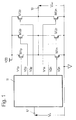
- a known output buffer which reduces the rate of transition of the output signal is illustrated in Figure 1.
- the buffer is constituted by three pairs of complementary MOS transistors (M1n, M1p; M2n, M2p; M3n, M3p) which are connected in a push-pull arrangement between two supply terminals, indicated by the ground symbol and +VDD, and which have their drain electrodes connected together to an output terminal 10.
- the gate electrode of each transistor is connected to a separate terminal of a generator 11 for generating phase-shifted voltages.
- the input 12 of the generator is also the input of the buffer.
- the input signal Vin changes from a low logic state to a high logic state
- a potential is thus established at the gate electrodes of the p-channel transistors such as to make the transistors M1p, M2p, M3p conductive one after another whilst the transistors M1n, M2n, M3n remain non-conductive.
- the object of the present invention is to provide an output buffer which can provide a digital output signal with edges having shallower slopes than the edges of the digital input signal and in which the slopes can be set precisely.
- FIG. 2 shows an inverter INV1 to which a digital input signal Vin is applied and which emits a corresponding output signal in the form of a current Ibi, a current-adding node A which adds a regulating current -If to the current Ibi coming from the inverter INV1, and a low-pass filter 20 which is constituted by a resistor R and by a capacitor C and which receives the current sum Idr as an input and supplies a voltage Vdr to the input of a second inverter INV2.
- the output 21 of the inverter INV2 is the output of the buffer and is connected to a circuit block 22 which can produce the differential of the output voltage Vout and multiply it by a constant K to produce the regulating current -If.
- the input 23 of the adder A may be considered as the true input of the buffer and the current Ibi as the electrical quantity input into the buffer.
- the electrical output quantity is the voltage Vout.
- the block 22 performs a measurement of the slope of the edge of the output signal and supplies it to the adder as a current If with the opposite sign to the sign of the input current Ibi.
- the resulting current Idr is applied to the low-pass filter 20 the output voltage of which is the input Vdr of the second inverter INV2.
- the circuit block 22 establishes a negative feedback which has the effect of stabilizing the slope of the edges of the output voltage and reducing its dependence on variations due to the process and to the supply and, partially, on variations due to the load and to the temperature.
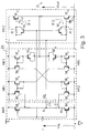
- circuit diagram of Figure 3 shows a practical embodiment of the buffer according to the invention. Although a precise identification of the blocks of the diagram of Figure 2 in the circuit diagram of Figure 3 is not possible, for reasons which will become clear from the following description, various parts of the circuit are enclosed by broken lines and indicated by the symbols and the reference numbers used in Figure 2 to show how the block diagram and the circuit diagram correspond.
- the inverter INV1 is constituted by two complementary MOS transistors M1 (n-channel) and M2 (p-channel) which are connected between the supply terminals, indicated +VDD and by the ground symbol, and which have their gate electrodes connected together to the input terminal of the circuit and their drain electrodes connected together to the input 23 of the buffer.
- the inverter INV2 is constituted by two complementary MOS transistors, that is, an n-channel MOS transistor M15 and a p-channel MOS transistor M16 connected in a push-pull arrangement between the supply terminals.
- the transistors M15 and M16 have their drain electrodes connected together to the output terminal 21 of the buffer and their gate electrodes connected to the input 23 of the buffer, each via a resistive unit identified R1, R2, respectively.
- the unit R1 is constituted by a resistor R1' and by a p-channel MOS transistor M13 connected in parallel with the resistor and the unit R2 is constituted by a resistor R2' and by an n-channel MOS transistor M14 connected in parallel with the resistor.
- the gate electrodes of the transistors M13 and M14 are connected together to the input of the inverter INV1.
- resistive units R1 and R2 are included in the block indicated as the inverter INV2, they form part of the low-pass filter indicated 20 in Figure 2.
- the parasitic input capacitances Cp and Cn of the transistors M16 and M15, which also form part of the low-pass filter 20 (and correspond to the capacitor C of Figure 2), are included in the same block.
- the differentiating circuit 22 is constituted by two capacitive elements formed, in this embodiment, by the gate-channel capacitances of two MOS transistors, a p-channel MOS transistor M10 and an n-channel MOS transistor M11, and by two capacitance multipliers constituted by four current mirrors MR1, MR2, MR3, MR4 having a predetermined gain, for example, of 2, connected as shown in the diagram of Figure 3.
- the transistor M1 of the inverter INV1 becomes conductive and the transistor M2 becomes non-conductive.
- the transistor M15 becomes non-conductive and transistor M16 becomes conductive.
- the output Vout of the inverter INV2, that is, the output of the buffer has the same sign as the input Vin but the slope of the leading edge is less than that of the input signal because the switching of the transistor M16 of the inverter INV2 which changes from non-conduction to conduction, is slowed by the charging of the input capacitance Cp through the resistive element R1.
- the resistance of the resistive element R1 depends on the conduction state of the transistor M13; in the embodiment described above, the gate electrode of the transistor M13 changes from a low level to a high level so that the transistor M13 becomes non-conductive and the resistance of the resistive element R1 is, in practice, that of the resistor R1'.
- the transistor M14 of the resistive element R2 which is an n-channel transistor, is made conductive by the same signal which controls the transistor M13.
- the transistor M14 thus becomes conductive so that the resistance of the resistive element R2 is practically zero (the resistance of the transistor M14 when it is conductive); this has the effect of a rapid switching of the transistor M15 (from conduction to non-conduction) so that the effect of slowing of the transition of the signal from the low level to the high level caused by the charging of the capacitance Cp through the resistor R1' is not affected.
- the operation of the circuit when the signal Vin has a transition from the high level to the low level is exactly the same but with the opposite sign.
- a current If of a magnitude dependent on the transition time is added, in the adding node A, to the input current Ibi supplied by one or other of the transistors M1, M2 of the inverter INV1 (in this example by M1).
- the sign of this current is always the opposite of that of the input current, owing to the crossed connection of the current mirrors.
- the current mirrors MR3 and MR2 constitute the path between the capacitance of M11 and the input and the current mirrors MR4 and MR1 constitute the path between the capacitance of M10 and the input.
- the buffer according to the invention not only enables the slope of the edges of the digital signal to be regulated automatically and precisely, rendering it substantially independent of variations due to the process by which the integrated circuit is produced and to environmental operating conditions, but can also be produced in a smaller area than is required by a known buffer with known regulation, such as that shown in Figure 1.
- resistors of constant resistance could be used instead of the resistive units R1 and R2, the resistance of which is dependent on the input signal, and true capacitors could be used instead of the capacitive units constituted by MOS transistors and capacitance multipliers.
Landscapes
- Physics & Mathematics (AREA)
- Engineering & Computer Science (AREA)
- Computer Hardware Design (AREA)
- Computing Systems (AREA)
- General Engineering & Computer Science (AREA)
- Mathematical Physics (AREA)
- Logic Circuits (AREA)
Priority Applications (2)
| Application Number | Priority Date | Filing Date | Title |
|---|---|---|---|
| EP99830634A EP1091492A1 (fr) | 1999-10-08 | 1999-10-08 | Tampon de sortie pour signaux numériques |
| US09/684,157 US6545503B1 (en) | 1999-10-08 | 2000-10-06 | Output buffer for digital signals |
Applications Claiming Priority (1)
| Application Number | Priority Date | Filing Date | Title |
|---|---|---|---|
| EP99830634A EP1091492A1 (fr) | 1999-10-08 | 1999-10-08 | Tampon de sortie pour signaux numériques |
Publications (1)
| Publication Number | Publication Date |
|---|---|
| EP1091492A1 true EP1091492A1 (fr) | 2001-04-11 |
Family
ID=8243619
Family Applications (1)
| Application Number | Title | Priority Date | Filing Date |
|---|---|---|---|
| EP99830634A Withdrawn EP1091492A1 (fr) | 1999-10-08 | 1999-10-08 | Tampon de sortie pour signaux numériques |
Country Status (2)
| Country | Link |
|---|---|
| US (1) | US6545503B1 (fr) |
| EP (1) | EP1091492A1 (fr) |
Cited By (3)
| Publication number | Priority date | Publication date | Assignee | Title |
|---|---|---|---|---|
| WO2003073451A3 (fr) * | 2002-02-21 | 2003-10-16 | Broadcom Corp | Procedes et systemes permettant de realiser une commande de courant de sortie adaptee a la charge |
| EP1880469A4 (fr) * | 2005-05-13 | 2008-06-11 | Packet Digital | Regulation de pics de courant transitoire |
| CN108563276A (zh) * | 2018-06-01 | 2018-09-21 | 电子科技大学 | 一种带有交叉耦合滤波网络的高速参考电压缓冲器 |
Families Citing this family (3)
| Publication number | Priority date | Publication date | Assignee | Title |
|---|---|---|---|---|
| US7521975B2 (en) * | 2005-01-20 | 2009-04-21 | Advanced Micro Devices, Inc. | Output buffer with slew rate control utilizing an inverse process dependent current reference |
| DE102005028173B4 (de) * | 2005-06-17 | 2007-03-08 | Texas Instruments Deutschland Gmbh | Integrierte CMOS-Tastverhältnis-Korrekturschaltung für ein Taktsignal |
| US10958271B1 (en) | 2020-07-07 | 2021-03-23 | Micron Technology, Inc. | Output buffer having supply filters |
Citations (4)
| Publication number | Priority date | Publication date | Assignee | Title |
|---|---|---|---|---|
| US5041741A (en) * | 1990-09-14 | 1991-08-20 | Ncr Corporation | Transient immune input buffer |
| WO1991020129A1 (fr) * | 1990-06-12 | 1991-12-26 | Robert Bosch Gmbh | Circuit pour la limitation de la vitesse de montee des signaux de sortie de circuits integres |
| US5111076A (en) * | 1990-09-05 | 1992-05-05 | Min Ming Tarng | Digital superbuffer |
| EP0678983A1 (fr) * | 1994-04-22 | 1995-10-25 | STMicroelectronics S.r.l. | Circuit intégré pour commander la vitesse de montée de courant d'un tampon de sortie |
Family Cites Families (4)
| Publication number | Priority date | Publication date | Assignee | Title |
|---|---|---|---|---|
| JPH07245546A (ja) * | 1994-03-03 | 1995-09-19 | Nippon Motorola Ltd | アクティブローパスフィルタ |
| US5543753A (en) * | 1994-06-22 | 1996-08-06 | Carver Corporation | Audio frequency power amplifiers with actively damped filter |
| US5805020A (en) * | 1996-06-27 | 1998-09-08 | Harris Corporation | Silent start class D amplifier |
| JP3745123B2 (ja) * | 1998-08-24 | 2006-02-15 | 三菱電機株式会社 | デューティ比補正回路及びクロック生成回路 |
-
1999
- 1999-10-08 EP EP99830634A patent/EP1091492A1/fr not_active Withdrawn
-
2000
- 2000-10-06 US US09/684,157 patent/US6545503B1/en not_active Expired - Lifetime
Patent Citations (4)
| Publication number | Priority date | Publication date | Assignee | Title |
|---|---|---|---|---|
| WO1991020129A1 (fr) * | 1990-06-12 | 1991-12-26 | Robert Bosch Gmbh | Circuit pour la limitation de la vitesse de montee des signaux de sortie de circuits integres |
| US5111076A (en) * | 1990-09-05 | 1992-05-05 | Min Ming Tarng | Digital superbuffer |
| US5041741A (en) * | 1990-09-14 | 1991-08-20 | Ncr Corporation | Transient immune input buffer |
| EP0678983A1 (fr) * | 1994-04-22 | 1995-10-25 | STMicroelectronics S.r.l. | Circuit intégré pour commander la vitesse de montée de courant d'un tampon de sortie |
Cited By (5)
| Publication number | Priority date | Publication date | Assignee | Title |
|---|---|---|---|---|
| WO2003073451A3 (fr) * | 2002-02-21 | 2003-10-16 | Broadcom Corp | Procedes et systemes permettant de realiser une commande de courant de sortie adaptee a la charge |
| US6690199B2 (en) | 2002-02-21 | 2004-02-10 | Broadcom Corporation | Methods and systems for providing load-adaptive output current drive |
| US6859069B2 (en) | 2002-02-21 | 2005-02-22 | Broadcom Corporation | Methods and systems for providing load-adaptive output current drive |
| EP1880469A4 (fr) * | 2005-05-13 | 2008-06-11 | Packet Digital | Regulation de pics de courant transitoire |
| CN108563276A (zh) * | 2018-06-01 | 2018-09-21 | 电子科技大学 | 一种带有交叉耦合滤波网络的高速参考电压缓冲器 |
Also Published As
| Publication number | Publication date |
|---|---|
| US6545503B1 (en) | 2003-04-08 |
Similar Documents
| Publication | Publication Date | Title |
|---|---|---|
| KR100231091B1 (ko) | 레벨 시프터 회로 | |
| US6642769B1 (en) | High speed voltage level shifter with a low input voltage | |
| KR20000070254A (ko) | 지연이 없는 슬루율 제어된 출력 버퍼 | |
| EP0129580A1 (fr) | Circuit de mise en forme d'impulsions d'horloge | |
| JP3338758B2 (ja) | 遅延回路 | |
| US4785262A (en) | Pulse generator producing pulses having a width free from a power voltage and a threshold voltage of an inverter used therein | |
| JP2743878B2 (ja) | 入力バッファ回路 | |
| US4617477A (en) | Symmetrical output complementary buffer | |
| JP4477705B2 (ja) | 差動増幅回路 | |
| US6937085B1 (en) | Sense amplifier based voltage comparator | |
| EP0015554B1 (fr) | Circuit comparateur | |
| EP0069444B1 (fr) | Générateur d'impulsions de commande | |
| EP1091492A1 (fr) | Tampon de sortie pour signaux numériques | |
| US4472645A (en) | Clock circuit for generating non-overlapping pulses | |
| KR20000028857A (ko) | 지연 회로 | |
| US6850100B2 (en) | Output buffer circuit | |
| US6346835B1 (en) | Power-on reset signal preparing circuit | |
| EP0845862A2 (fr) | Circuit servant à soustraire les composantes de bruit d'un oscillateur | |
| US20020180505A1 (en) | Pulsed signal transition delay adjusting circuit | |
| US4837463A (en) | Three-state complementary field effect integrated circuit | |
| EP1292031A2 (fr) | Circuit intégré et méthode pour ajuster la capacité d'un noeud de circuit intégré | |
| EP0720296A2 (fr) | Circuit tampon et circuit de polarisation | |
| WO1988008228A2 (fr) | Procede et appareil pour attenuer les bruits occasionnels dans les circuits integres | |
| KR20010004448A (ko) | 고전압 출력 인버터 | |
| KR100430973B1 (ko) | 2개의전기값을비교하기위한회로 |
Legal Events
| Date | Code | Title | Description |
|---|---|---|---|
| PUAI | Public reference made under article 153(3) epc to a published international application that has entered the european phase |
Free format text: ORIGINAL CODE: 0009012 |
|
| AK | Designated contracting states |
Kind code of ref document: A1 Designated state(s): DE FR GB IT |
|
| AX | Request for extension of the european patent |
Free format text: AL;LT;LV;MK;RO;SI |
|
| 17P | Request for examination filed |
Effective date: 20010918 |
|
| AKX | Designation fees paid |
Free format text: DE FR GB IT |
|
| GRAP | Despatch of communication of intention to grant a patent |
Free format text: ORIGINAL CODE: EPIDOSNIGR1 |
|
| STAA | Information on the status of an ep patent application or granted ep patent |
Free format text: STATUS: THE APPLICATION IS DEEMED TO BE WITHDRAWN |
|
| 18D | Application deemed to be withdrawn |
Effective date: 20080219 |