EP0720296A2 - Circuit tampon et circuit de polarisation - Google Patents
Circuit tampon et circuit de polarisation Download PDFInfo
- Publication number
- EP0720296A2 EP0720296A2 EP95308445A EP95308445A EP0720296A2 EP 0720296 A2 EP0720296 A2 EP 0720296A2 EP 95308445 A EP95308445 A EP 95308445A EP 95308445 A EP95308445 A EP 95308445A EP 0720296 A2 EP0720296 A2 EP 0720296A2
- Authority
- EP
- European Patent Office
- Prior art keywords
- node
- terminal
- transistor
- terminal connected
- source
- Prior art date
- Legal status (The legal status is an assumption and is not a legal conclusion. Google has not performed a legal analysis and makes no representation as to the accuracy of the status listed.)
- Granted
Links
- 230000000295 complement effect Effects 0.000 claims description 6
- 238000004519 manufacturing process Methods 0.000 description 8
- 230000008859 change Effects 0.000 description 5
- 230000004044 response Effects 0.000 description 5
- 230000007423 decrease Effects 0.000 description 4
- 230000009467 reduction Effects 0.000 description 3
- 230000008901 benefit Effects 0.000 description 2
- 238000010586 diagram Methods 0.000 description 2
- 230000005669 field effect Effects 0.000 description 2
- 238000012986 modification Methods 0.000 description 2
- 230000004048 modification Effects 0.000 description 2
- 239000004065 semiconductor Substances 0.000 description 2
- 230000003247 decreasing effect Effects 0.000 description 1
- 238000000034 method Methods 0.000 description 1
- 230000008569 process Effects 0.000 description 1
- 230000000630 rising effect Effects 0.000 description 1
- 239000000758 substrate Substances 0.000 description 1
Images

Classifications
-
- H—ELECTRICITY
- H03—ELECTRONIC CIRCUITRY
- H03K—PULSE TECHNIQUE
- H03K19/00—Logic circuits, i.e. having at least two inputs acting on one output; Inverting circuits
-
- G—PHYSICS
- G05—CONTROLLING; REGULATING
- G05F—SYSTEMS FOR REGULATING ELECTRIC OR MAGNETIC VARIABLES
- G05F3/00—Non-retroactive systems for regulating electric variables by using an uncontrolled element, or an uncontrolled combination of elements, such element or such combination having self-regulating properties
- G05F3/02—Regulating voltage or current
- G05F3/08—Regulating voltage or current wherein the variable is DC
- G05F3/10—Regulating voltage or current wherein the variable is DC using uncontrolled devices with non-linear characteristics
- G05F3/16—Regulating voltage or current wherein the variable is DC using uncontrolled devices with non-linear characteristics being semiconductor devices
- G05F3/20—Regulating voltage or current wherein the variable is DC using uncontrolled devices with non-linear characteristics being semiconductor devices using diode- transistor combinations
- G05F3/24—Regulating voltage or current wherein the variable is DC using uncontrolled devices with non-linear characteristics being semiconductor devices using diode- transistor combinations wherein the transistors are of the field-effect type only
- G05F3/242—Regulating voltage or current wherein the variable is DC using uncontrolled devices with non-linear characteristics being semiconductor devices using diode- transistor combinations wherein the transistors are of the field-effect type only with compensation for device parameters, e.g. channel width modulation, threshold voltage, processing, or external variations, e.g. temperature, loading, supply voltage
-
- G—PHYSICS
- G05—CONTROLLING; REGULATING
- G05F—SYSTEMS FOR REGULATING ELECTRIC OR MAGNETIC VARIABLES
- G05F3/00—Non-retroactive systems for regulating electric variables by using an uncontrolled element, or an uncontrolled combination of elements, such element or such combination having self-regulating properties
- G05F3/02—Regulating voltage or current
- G05F3/08—Regulating voltage or current wherein the variable is DC
- G05F3/10—Regulating voltage or current wherein the variable is DC using uncontrolled devices with non-linear characteristics
- G05F3/16—Regulating voltage or current wherein the variable is DC using uncontrolled devices with non-linear characteristics being semiconductor devices
- G05F3/20—Regulating voltage or current wherein the variable is DC using uncontrolled devices with non-linear characteristics being semiconductor devices using diode- transistor combinations
- G05F3/24—Regulating voltage or current wherein the variable is DC using uncontrolled devices with non-linear characteristics being semiconductor devices using diode- transistor combinations wherein the transistors are of the field-effect type only
-
- H—ELECTRICITY
- H03—ELECTRONIC CIRCUITRY
- H03K—PULSE TECHNIQUE
- H03K19/00—Logic circuits, i.e. having at least two inputs acting on one output; Inverting circuits
- H03K19/003—Modifications for increasing the reliability for protection
- H03K19/00369—Modifications for compensating variations of temperature, supply voltage or other physical parameters
- H03K19/00384—Modifications for compensating variations of temperature, supply voltage or other physical parameters in field effect transistor circuits
-
- H—ELECTRICITY
- H03—ELECTRONIC CIRCUITRY
- H03K—PULSE TECHNIQUE
- H03K19/00—Logic circuits, i.e. having at least two inputs acting on one output; Inverting circuits
- H03K19/0175—Coupling arrangements; Interface arrangements
- H03K19/0185—Coupling arrangements; Interface arrangements using field effect transistors only
- H03K19/018507—Interface arrangements
- H03K19/018521—Interface arrangements of complementary type, e.g. CMOS
- H03K19/018528—Interface arrangements of complementary type, e.g. CMOS with at least one differential stage
Definitions
- This invention relates particularly to a buffer circuit and a bias circuit both of which electrically process signals such as small amplitude signals (each corresponding to a signal in which the difference between a voltage level indicative of a high logical level and a voltage level indicative of a low logical level is small, such as a signal whose amplitude is of 200mV with a substantially central level between a ground potential and 2V as the center when a source potential level is of 2V).
- signals such as small amplitude signals (each corresponding to a signal in which the difference between a voltage level indicative of a high logical level and a voltage level indicative of a low logical level is small, such as a signal whose amplitude is of 200mV with a substantially central level between a ground potential and 2V as the center when a source potential level is of 2V).
- This type of buffer circuit includes a transistor provided on the signal input side and a transistor provided on the signal output side.
- a small amplitude signal having a voltage level in the vicinity of a threshold voltage of a transistor thereof is inputted to the signal input side transistor.
- a small amplitude signal having a voltage level in the vicinity of a threshold voltage of a transistor provided within an external circuit for receiving the output of the buffer circuit therein is outputted from the signal output side transistor.
- the buffer circuit which electrically handles the small amplitude signals referred to above, can transfer signals at high speed as compared with a buffer circuit composed of transistors whose switching operations are performed in the saturation region.
- the buffer circuit is used particularly in an electronic circuit that needs a high-speed operation.
- a typical buffer circuit comprising a first transistor having a first terminal connected to a current source, a second terminal connected to a first node and a control electrode connected to a first input terminal for receiving a first input signal; a second transistor having a first terminal connected to the current source, a second terminal connected to a second node and a control electrode connected to a second input terminal for receiving a second input signal; a third transistor having a first terminal connected to a first source node supplied with a first source potential level, a second terminal connected to the first node and a control electrode connected to a first output terminal; a fourth transistor having a first terminal connected to the first source node, a second terminal connected to the second node and a control electrode connected to a second output terminal; a fifth transistor having a first terminal connected to the first output terminal, a second terminal connected to the first source node and a control electrode connected to the first node; and a sixth transistor having a
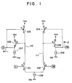
- Fig. 1 is a circuit diagram showing one embodiment of a buffer circuit according to the present invention.
- the buffer circuit inputs and outputs small amplitude signals and is composed of field effect transistors (hereinafter called simply "MOS transistors") formed on a semiconductor substrate.
- the buffer circuit inputs complementary small amplitude signals received at input terminals D and DB and outputs complementary small amplitude signals corresponding to the small amplitude signals from output terminals O and OB without being affected by variations in threshold voltages of the MOS transistors.
- each of the small amplitude signals shows a signal in which the difference between a voltage level indicative of a high logical level and a voltage level indicative of a low logical level is small.
- the small amplitude signal means a signal whose amplitude is of 200mV with a substantially central level between a ground potential and 2V as the center.
- the buffer circuit includes NMOSs 101 and 102 to which the complementary small amplitude signals are inputted, and a current source 108.
- the NMOSs 101 and 102 have the same dimension (which is defined by a gate length W and a gate width L, for example).
- the NMOS 101 has a gate G electrically connected to the input terminal D supplied with one of the complementary signals, a drain D electrically connected to a node 110 and a source S electrically connected to the current source 108.
- the NMOS 102 has a gate G electrically connected to the input terminal DB supplied with the other of the complementary signals, a drain D electrically connected to a node 111 and a source S electrically connected to the current source 108.
- the current source 108 is electrically connected between the sources S of the NMOSs 101 and 102 and the ground potential V ss .
- the buffer circuit further includes negative feedback controlled PMOSs 103 and 104.
- the PMOSs 103 and 104 have the same dimension (which is defined by a gate length W and a gate width L, for example).
- the PMOS 103 has a source S electrically connected to a source potential V cc , a drain D electrically connected to the node 110 and a gate G electrically connected to a node ⁇ 1-1 connected to the output terminal O.
- the PMOS 104 has a source S electrically connected to the source potential V cc , a drain D electrically connected to the node 111 and a gate G electrically connected to a node ⁇ 1-2 connected to the output terminal OB.
- the value of a resistance between the source S and drain D of the PMOS 103 is controlled by a potential which appears at the node ⁇ 1-1.
- the value of a resistance between the source S and drain D of the PMOS 104 is controlled by a potential which appears at the node ⁇ 1-2.
- the buffer circuit includes NMOSs 105 and 106, a current source 107 and a current source 109.
- the NMOSs 105 and 106 have the same dimension (which is defined by a gate length W and a gate width L, for example).
- the NMOS 105 has a drain D electrically connected to the source potential V cc , a source S electrically connected to the node ⁇ 1-1 and a gate G electrically connected to the node 110.
- the NMOS 106 has a drain D electrically connected to the source potential V cc , a source S electrically connected to the node ⁇ 1-2 and a gate G electrically connected to the node 111.
- the current source 107 is electrically connected between the source S of the NMOS 105 and the ground potential V ss .
- the current source 109 is electrically connected between the source S of the NMOS 106 and the ground potential V ss .
- the potential at the node 110 is reduced.
- the potential applied to the gate G of the NMOS 105 is reduced.
- the value of a resistance between the source S and drain D of the NMOS 105 increases.
- the potential at the node ⁇ 1-1 becomes a potential determined by the current source 107. Namely, the voltage at the output node ⁇ 1-1 is also reduced in response to the potential at the node 110.
- the resistance between the source S and drain D of the PMOS 103 is reduced.
- a current that flows between the source S and drain D of the PMOS 103 increases.
- the resistance between the source S and drain D of the PMOS 103 is lowered, the potential at the node 110 tends to rise.
- the NMOS 105 provides negative feedback to avoid an excessive reduction in potential at the output node ⁇ 1-1. It is thus possible to output a stable small amplitude signal from the output terminal O.
- the potential at the input terminal DB is low at this time, the potential applied to the gate G of the NMOS 102 becomes lower than that applied to the gate G of the NMOS 101. As a result, the current that flows between the source S and drain D of the NMOS 102 decreases. Thus, since the potential at the node 111 rises and the potential of the gate G of the NMOS 106 is raised, a current that flows between the source S and drain D of the NMOS 106, increases. Accordingly, the potential at the output node ⁇ 1-2 is also increased in response to the potential at the node 111.
- the present embodiment Since the potential at the gate G of the PMOS 104 activated as a variable resistor in the non-saturation region rises as the potential at the output node ⁇ 1-2 increases, a current which flows between the source S and drain D of the PMOS 104, is reduced. When the current is decreased, the potential at the node 111 tends to drop. In response to the drop in potential at the node 111, the NMOS 106 provides negative feedback to avoid an excessive rise in potential at the output node ⁇ 1-2.
- a small amplitude signal stable toward a variation in threshold voltage of each transistor can be obtained from the output terminal OB.
- the negative feedback is provided after the level of the output node has varied. Namely, the present embodiment is capable of operating at quicker speed because it is not affected by initial variations in levels of the nodes 110 and 111.
- each of threshold voltages of transistors is deviate from a target value (design value).
- a target value design value
- the threshold voltages of the transistors are deviate from the target value.
- the first case may be mentioned a case where the threshold voltage V tp of the PMOS 103 included in a portion on the left side of the circuit shown in Fig. 1 becomes greater than the target value and the potential at the node 110 becomes lower than the target value. Since the potential at the output node ⁇ 1-1 is also lower than the target value at this time, more current flows in the PMOS 103. As a result, the potential at the node 110 can be prevented from dropping.
- the PMOS 104 included in a portion on the right side of the circuit shown in Fig. 1 is also activated in a manner similar to the PMOS 103.
- the second case corresponds to a case in which the threshold voltage V tp of the PMOS 103 included in the portion on the left side of the circuit shown in Fig. 1 becomes lower than the target value and the potential at the node 110 becomes higher than the target value. Since the potential at the output node ⁇ 1-1 also rises at this time, the current that flows through the PMOS 103 is restricted so that a rise in potential applied to the node 110 can be suppressed. Further, the PMOS 104 included in the portion on the right side of the circuit shown in Fig. 1 is also activated in a manner similar to the PMOS 103.
- the third case shows a case where the threshold voltage V tn of the NMOS 101 included in the portion on the left side of the circuit shown in Fig. 1 becomes lower than the target value and the potential at the output node ⁇ 1-1 becomes lower than the target value.
- V tn of the NMOS 101 included in the portion on the left side of the circuit shown in Fig. 1 becomes lower than the target value and the potential at the output node ⁇ 1-1 becomes lower than the target value.
- more current flows through the PMOS 103 so that the potential at the node 110 is increased.
- the NMOS 105 tends to turn on easier as the potential at the node 110 increases, the potential applied to the output node ⁇ 1-1 can be prevented from dropping.
- the NMOS 102 included in the portion on the right side of the circuit shown in Fig. 1 is also activated in the same manner as described above.
- the fourth case shows a case where the threshold voltage V tn of the NMOS 101 included in the portion on the left side of the circuit shown in Fig. 1 becomes higher than the target value and the potential applied to the output node ⁇ 1-1 becomes greater than the target value.
- the current that flows through the PMOS 103 is restricted so that the potential at the node 110 is reduced.
- the NMOS 105 tends to turn off easier as the potential at the node 110 decreases, a rise in potential applied to the output node ⁇ 1-1 can be suppressed.
- the NMOS 102 included in the portion on the right side of the circuit shown in Fig. 1 is also activated in the same manner as described above.
- the threshold voltages (V tn and V tp ) of the transistors are deviate from the target value, it is possible to compensate for the current that flows in each of the nodes 110 and 111. Therefore, the potential of the small amplitude signal outputted from each of the output terminals O and OB has a less deviation from the target value.
- the negative feedback is provided so as to prevent the level of each output node from excessively rising and dropping. Since the negative feedback is provided after the level of each output node has varied, the buffer circuit can be activated at quicker speed.
- the values of the resistances between the source S and drain D of the PMOS 103 and between the source S and drain D of the PMOS 104 are suitably adjusted so as to compensate for the deviations.
- the potentials applied to the gates G of the NMOSs 105 and 106 can be adjusted so that influences exerted on the small amplitude signals outputted from the output terminals O and OB are less provided.
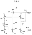
- Fig. 2 shows a bias circuit 10 according to the present invention.
- the bias circuit 10 also includes a negative feedback circuit thereinside.
- the bias circuit 10 is of a bias circuit provided with an output terminal VRPG for outputting a bias voltage independent on variations in threshold voltages of transistors and an output terminal VRNG for outputting a bias voltage independent on a source potential V cc .
- the bias circuit 10 is composed of a PMOS 201, NMOSs 202 through 206 and a resistor 208.
- the PMOS 201 has a source S electrically connected to the source potential V cc , a drain D electrically connected to a node 207 and a gate G electrically connected to the output terminal VRPG through an output node ⁇ 2-1.
- the NMOSs 202 and 203 are of transistors identical in dimension to each other and whose drains D and gates G are respectively electrically connected to the source potential V cc and the node 207.
- the NMOS 202 has a source S electrically connected to a drain D of the NMOS 204 through the resistor 208.
- the NMOS 203 has a source S electrically connected to a drain D of the NMOS 206 and the output node ⁇ 2-1 so that the PMOS 201 is controlled under negative feedback. Since the PMOS 201 and the NMOS 203 are electrically connected in the above-described manner, the bias voltage to be outputted from the output terminal VRPG can be outputted as a voltage independent on threshold voltages of these PMOS 201 and NMOS 203.
- the NMOSs 204 and 206 are of transistors identical in dimension to each other.
- the NMOSs 204 and 206 respectively have sources S electrically connected to a ground potential V ss and gates G electrically connected to the output terminal VRNG through an output node ⁇ 2-2. Further, the gate G of the NMOS 204 is also electrically connected to its own drain D.
- the NMOS 205 has a source S electrically connected to the ground potential Vss, a drain D electrically connected to the node 207 and a gate G electrically connected to the output terminal VRNG through the output node ⁇ 2-2.
- a threshold voltage Vt of a PMOS or NMOS is deviate from a target value.
- the first case may be mentioned a case where the absolute value of a threshold voltage V tp of the PMOS 201 becomes higher than the target value.
- a conducting state of the PMOS 201 becomes weak as compared with the time when the threshold voltage V tp is of the target value. Therefore, the potential at the node 207 is reduced as compared with the time when the threshold voltage V tp is of the target value.
- the potential applied to the gate G of the NMOS 203 becomes lower than the target value, the level of the potential applied to the output node ⁇ 2-1 is also reduced.
- the second case shows a case in which the absolute value of the threshold voltage V tp of the PMOS 201 becomes lower than the target value and the potential level of the node 207 becomes higher than the target value.
- negative feedback is provided for increasing the potential level of the output node ⁇ 2-1 and restricting the flow of the current through the PMOS 21 so as to suppress a rise in potential level of the node 207.
- the third case shows a case where a threshold voltage Vtn of the NMOS 203 becomes lower than the target value and the potential level of the output node ⁇ 2-1 becomes higher than the target value.
- negative feedback is provided for reducing the potential level of the node 207 and suppressing a rise in potential level of the output node ⁇ 2-1.
- the fourth case shows a case in which the threshold voltage V tn of the NMOS 203 becomes higher than the target value and the potential level of the output node ⁇ 2-1 becomes lower than the target value.
- negative feedback is provided for increasing the potential level of the node 207 and preventing the potential level of the output node ⁇ 2-1 from reduction.
- the output node ⁇ 2-1 is less affected by ⁇ V tp and ⁇ V tn defined in a range of variations in threshold voltages of the transistors owing to the negative feedback provided for the PMOS 201. It is therefore possible to output a constant voltage insensitive to the variations in threshold voltages of the transistors from the output terminal VRPG.
- a current iR that flows through the output node ⁇ 2-1 is equal to a current iL that flows through the output node ⁇ 2-2.
- iL iR
- V s of a voltage applied to a node s is equal to a value V rpg of a voltage applied to the output node ⁇ 2-1.
- V s V rpg
- the voltage value V rpg is equal to a voltage obtained by subtracting a voltage drop V no developed across the NMOS 203 from the source potential V cc .
- V rpg V cc - V no
- V ro R*iL
- V rng V cc (1 - kR) - V no
- V rng V cc (1 - kR) - V no
- a reference level Vrpg less affected by ⁇ V tp and ⁇ V tn can be obtained by electrically connecting the gate G of the PMOS 201 to the drain D of the NMOS 203 and electrically connecting the drain D of the PMOS 201 and the gate G of the NMOS 203 to each other.
- Fig. 3 is a circuit diagram showing a second embodiment of a bias circuit.
- the bias circuit is of a bias circuit provided with an input/output terminal VRN and an output terminal VRNN.
- the present bias circuit is composed of the bias circuit 10 shown in Fig. 2 and transistors of NMOSs 301 and 302.
- the input/output terminal VRN is electrically connected to the output terminal VRNG of the bias circuit 10.
- the NMOS 301 has a gate G electrically connected to the input/output terminal VRN, a drain D electrically connected to the output terminal VRNN and a source S electrically connected to a ground potential V ss .
- the NMOS 302 has a drain D and a gate G both electrically connected to a source potential V cc and a source S electrically connected to the output terminal VRNN.
- the voltage applied to the drain D of the NMOS 204 rises as the threshold voltage V tn of the NMOS 204 shown in Fig. 2 becomes greater than a target value. Therefore, the voltage at the input/output terminal VRNG is also raised in response to the voltage rise referred to above. Accordingly, the voltage at the input/output terminal VRN is also increased.
- the NMOS 301 is also placed under the influence of a variation in manufacture or a change in temperature characteristic, which is similar to the threshold voltage V tn of the NMOS 204.
- the state of conduction of the NMOS 301 is substantially equivalent to that at the time that the threshold voltage V tn is of the target value.
- a current, which flows between the source S and drain D of the NMOS 301 remains unchanged.
- a voltage V GS of the NMOS 302 becomes large as the threshold voltage V tn increases. Since a voltage V g applied to the gate G of the NMOS 302 is of V cc , the output terminal VRNN is supplied with a reference level reduced by ⁇ V tn when the threshold voltage V tn rises.
- the reference level reduced by the rise in threshold voltage V tn when the threshold voltage V tn becomes higher than the target value can be obtained at the output terminal VRNN by electrically connecting the input/output terminal VRN to the output terminal VRNG of the bias circuit 10, electrically connecting the gate G of the NMOS 301 to the input/output terminal VRN, electrically connecting the drain D of the NMOS 301 to the source S of the NMOS 302 and electrically connecting a node between both the drain D thereof and the source S thereof to the output terminal VRNN.
- the dependence of the central potential between the potentials of the small amplitude signals outputted from the nodes ⁇ 1-1 and ⁇ 1-2 on the threshold voltage V tn can be reduced by applying the reference level having a negative dependence on the variation in threshold voltage V tn to each of the current sources 107 and 109 in the buffer circuit shown in Fig. 1 by way of example.
- Fig. 4 shows a third embodiment of a bias circuit.
- the bias circuit comprises the bias circuit 10 shown in Fig. 2, an NMOS 401 and a PMOS 402.
- the PMOS 402 has a source S electrically connected to a source potential V cc , a gate G electrically connected to the output terminal VRPG of the bias circuit 10 and a drain D electrically connected to an output terminal VRN.
- the NMOS 401 has a source S electrically connected to a ground potential V ss and a drain D and a gate G both electrically connected to the output terminal VRN.
- a reference level at the output terminal VRPG of the bias circuit 10 does not depend on the threshold voltages V tn and V tp of the transistors that form the bias circuit 10.
- a current that flows through the PMOS 402 is reduced.
- a reference level at the output terminal VRN is lowered by a change in threshold voltage V tp .
- the threshold voltage V tn becomes higher than the target value, the value of a resistance between the source S and drain D of the NMOS 401 becomes great.
- the reference level at the output terminal VRN is increased by a change in threshold voltage Vtn.
- the gate G of the PMOS 402 is electrically connected to the output terminal VRPG of the bias circuit 10 and the drain D of the PMOS 402 and the drain D and gate G of the NMOS 401 are respectively electrically connected to the output terminal VRN, the reference level reduced by the change in threshold voltage V tp of the PMOS transistor can be obtained as the level of the output terminal VRN when the threshold voltage V tp thereof rises and the reference level increased by the change in threshold voltage V tn of the NMOS transistor can be obtained as the level of the output terminal VRN when the threshold voltage V tn thereof increases.
- the bias circuits shown in Figs. 2, 3 and 4 can be used to control the current source or the like of the buffer circuit shown in Fig. 1. However, the influence of an output against the deviations form the threshold voltages due to variations in manufacture and variations in temperature characteristics can be reduced by using the bias circuits to control current sources such as a voltage control type delay cell, etc.
- the signal having the potential level which approximates to the target value can be outputted even when the threshold voltage varies due to the variations in manufacture or the like.
- the stable small amplitude signal can be outputted by performing the control of the negative feedback over the potential on the output side.
- the stable bias voltage can be outputted by performing the control of the negative feedback over the potential on the output side.
- the bias voltage independent on the variation in source potential can be outputted by setting the resistance value of the resistor to the sufficient large value.
Landscapes
- Engineering & Computer Science (AREA)
- Physics & Mathematics (AREA)
- Microelectronics & Electronic Packaging (AREA)
- Computer Hardware Design (AREA)
- Computing Systems (AREA)
- Mathematical Physics (AREA)
- General Engineering & Computer Science (AREA)
- Nonlinear Science (AREA)
- Electromagnetism (AREA)
- General Physics & Mathematics (AREA)
- Radar, Positioning & Navigation (AREA)
- Automation & Control Theory (AREA)
- Logic Circuits (AREA)
- Amplifiers (AREA)
Applications Claiming Priority (3)
| Application Number | Priority Date | Filing Date | Title |
|---|---|---|---|
| JP322327/94 | 1994-12-26 | ||
| JP32232794 | 1994-12-26 | ||
| JP32232794A JP3158000B2 (ja) | 1994-12-26 | 1994-12-26 | バイアス回路 |
Publications (3)
| Publication Number | Publication Date |
|---|---|
| EP0720296A2 true EP0720296A2 (fr) | 1996-07-03 |
| EP0720296A3 EP0720296A3 (fr) | 1997-04-16 |
| EP0720296B1 EP0720296B1 (fr) | 2001-08-16 |
Family
ID=18142406
Family Applications (1)
| Application Number | Title | Priority Date | Filing Date |
|---|---|---|---|
| EP95308445A Expired - Lifetime EP0720296B1 (fr) | 1994-12-26 | 1995-11-24 | Circuit tampon et circuit de polarisation |
Country Status (6)
| Country | Link |
|---|---|
| US (2) | US5648734A (fr) |
| EP (1) | EP0720296B1 (fr) |
| JP (1) | JP3158000B2 (fr) |
| KR (1) | KR100363139B1 (fr) |
| DE (1) | DE69522196T2 (fr) |
| TW (1) | TW453023B (fr) |
Families Citing this family (7)
| Publication number | Priority date | Publication date | Assignee | Title |
|---|---|---|---|---|
| US5909127A (en) * | 1995-12-22 | 1999-06-01 | International Business Machines Corporation | Circuits with dynamically biased active loads |
| US7173474B1 (en) | 1999-09-15 | 2007-02-06 | Linear Technology Corporation | Load-generated drive, no quiescent current, techniques and circuits for high speed switching of transistors |
| US6531909B1 (en) * | 1999-09-15 | 2003-03-11 | Linear Technology Corporation | Load-generated drive, substantially no quiescent current, techniques and circuits for high speed switching of transistors |
| DE60123062T2 (de) * | 2000-07-03 | 2007-04-19 | Broadcom Corp., Irvine | Vorspannungsschaltung zum erzeugung von mehreren vorspannungen |
| US6522174B2 (en) * | 2001-04-16 | 2003-02-18 | Intel Corporation | Differential cascode current mode driver |
| US6791356B2 (en) * | 2001-06-28 | 2004-09-14 | Intel Corporation | Bidirectional port with clock channel used for synchronization |
| CN1311628C (zh) * | 2001-08-16 | 2007-04-18 | 皇家飞利浦电子股份有限公司 | 差分环形振荡器级 |
Family Cites Families (23)
| Publication number | Priority date | Publication date | Assignee | Title |
|---|---|---|---|---|
| US3970875A (en) * | 1974-11-21 | 1976-07-20 | International Business Machines Corporation | LSI chip compensator for process parameter variations |
| JPS562017A (en) * | 1979-06-19 | 1981-01-10 | Toshiba Corp | Constant electric current circuit |
| NL8001560A (nl) * | 1980-03-17 | 1981-10-16 | Philips Nv | Stroomstabilisator opgebouwd met veldeffekttransistor van het verrijkingstype. |
| GB2093303B (en) * | 1981-01-20 | 1985-05-22 | Citizen Watch Co Ltd | Voltage sensing circuit |
| US4450371A (en) * | 1982-03-18 | 1984-05-22 | Rca Corporation | Speed up circuit |
| JPS59191936A (ja) * | 1983-04-15 | 1984-10-31 | Nec Corp | 高速論理回路 |
| US4570084A (en) * | 1983-11-21 | 1986-02-11 | International Business Machines Corporation | Clocked differential cascode voltage switch logic systems |
| US4616189A (en) * | 1985-04-26 | 1986-10-07 | Triquint Semiconductor, Inc. | Gallium arsenide differential amplifier with closed loop bias stabilization |
| JPS62234705A (ja) * | 1986-04-03 | 1987-10-15 | Toyota Motor Corp | 自動車の懸架装置 |
| JP2559032B2 (ja) * | 1986-09-13 | 1996-11-27 | 富士通株式会社 | 差動増幅回路 |
| JPS63234705A (ja) * | 1987-03-24 | 1988-09-30 | Matsushita Electric Ind Co Ltd | 差動増幅器 |
| US4994688A (en) * | 1988-05-25 | 1991-02-19 | Hitachi Ltd. | Semiconductor device having a reference voltage generating circuit |
| DE3884620T2 (de) * | 1988-06-30 | 1994-02-03 | Alcatel Nv | Elektronische anordnungen und signalvergleichsvorrichtung, die diese verwendet. |
| KR910001068B1 (ko) * | 1988-07-11 | 1991-02-23 | 삼성전자 주식회사 | 메모리장치의 공급전압 안정화회로 |
| US5045807A (en) * | 1988-11-21 | 1991-09-03 | Nippon Telegraph And Telephone Corporation | Amplifier circuit using feedback load |
| EP0397408A1 (fr) * | 1989-05-09 | 1990-11-14 | Advanced Micro Devices, Inc. | Générateur de tension de référence |
| JPH05167427A (ja) * | 1991-12-13 | 1993-07-02 | Toshiba Corp | レベルシフト回路 |
| US5309039A (en) * | 1992-09-29 | 1994-05-03 | Motorola, Inc. | Power supply dependent input buffer |
| US5486778A (en) * | 1993-03-10 | 1996-01-23 | Brooktree Corporation | Input buffer for translating TTL levels to CMOS levels |
| US5488321A (en) * | 1993-04-07 | 1996-01-30 | Rambus, Inc. | Static high speed comparator |
| JP2531104B2 (ja) * | 1993-08-02 | 1996-09-04 | 日本電気株式会社 | 基準電位発生回路 |
| US5399960A (en) * | 1993-11-12 | 1995-03-21 | Cypress Semiconductor Corporation | Reference voltage generation method and apparatus |
| US5654665A (en) * | 1995-05-18 | 1997-08-05 | Dynachip Corporation | Programmable logic bias driver |
-
1994
- 1994-12-26 JP JP32232794A patent/JP3158000B2/ja not_active Expired - Fee Related
-
1995
- 1995-11-24 DE DE69522196T patent/DE69522196T2/de not_active Expired - Lifetime
- 1995-11-24 EP EP95308445A patent/EP0720296B1/fr not_active Expired - Lifetime
- 1995-11-24 TW TW084112533A patent/TW453023B/zh not_active IP Right Cessation
- 1995-12-04 US US08/566,955 patent/US5648734A/en not_active Expired - Lifetime
- 1995-12-26 KR KR1019950056727A patent/KR100363139B1/ko not_active Expired - Fee Related
-
1997
- 1997-03-03 US US08/810,284 patent/US5739719A/en not_active Expired - Lifetime
Non-Patent Citations (1)
| Title |
|---|
| None |
Also Published As
| Publication number | Publication date |
|---|---|
| JPH08181549A (ja) | 1996-07-12 |
| KR100363139B1 (ko) | 2003-02-11 |
| JP3158000B2 (ja) | 2001-04-23 |
| EP0720296B1 (fr) | 2001-08-16 |
| DE69522196T2 (de) | 2002-04-18 |
| EP0720296A3 (fr) | 1997-04-16 |
| KR960027331A (ko) | 1996-07-22 |
| DE69522196D1 (de) | 2001-09-20 |
| US5739719A (en) | 1998-04-14 |
| TW453023B (en) | 2001-09-01 |
| US5648734A (en) | 1997-07-15 |
Similar Documents
| Publication | Publication Date | Title |
|---|---|---|
| US4952818A (en) | Transmission line driver circuits | |
| US4894561A (en) | CMOS inverter having temperature and supply voltage variation compensation | |
| EP0110701B1 (fr) | Circuit tampon d'entrée | |
| US4275313A (en) | Current limiting output circuit with output feedback | |
| EP0405319B1 (fr) | Circuit de retard présentant un retard stable | |
| US4380710A (en) | TTL to CMOS Interface circuit | |
| US20050270077A1 (en) | Method and apparatus for providing a power-on reset signal | |
| JPH06204838A (ja) | 基準電圧発生器及び基準電圧の発生方法 | |
| JPH0119297B2 (fr) | ||
| US4071784A (en) | MOS input buffer with hysteresis | |
| EP0121793B1 (fr) | Circuits CMOS comportant un régulateur de tension adapté à un paramètre | |
| US4369381A (en) | CMOS Schmitt-trigger circuit | |
| US6236195B1 (en) | Voltage variation correction circuit | |
| EP0720296B1 (fr) | Circuit tampon et circuit de polarisation | |
| US6985014B2 (en) | System and method for compensating for the effects of process, voltage, and temperature variations in a circuit | |
| EP0438706A2 (fr) | Circuit d'attaque CMOS à haute vitesse de commutation | |
| JPH06230840A (ja) | バイアス回路 | |
| US6975168B2 (en) | Drive circuit | |
| US20100073037A1 (en) | Output impedance control circuit | |
| US6175267B1 (en) | Current compensating bias generator and method therefor | |
| EP0417985A2 (fr) | Amplificateur inverseur à amplitude stabilisée | |
| US5963076A (en) | Circuit with hot-electron protection and method | |
| US5296754A (en) | Push-pull circuit resistant to power supply and temperature induced distortion | |
| EP0499645A1 (fr) | Circuit amplificateur differentiel dans un amplificateur operationnel | |
| JPH02177724A (ja) | 出力バッファ回路 |
Legal Events
| Date | Code | Title | Description |
|---|---|---|---|
| PUAI | Public reference made under article 153(3) epc to a published international application that has entered the european phase |
Free format text: ORIGINAL CODE: 0009012 |
|
| AK | Designated contracting states |
Kind code of ref document: A2 Designated state(s): DE FR GB NL |
|
| PUAL | Search report despatched |
Free format text: ORIGINAL CODE: 0009013 |
|
| AK | Designated contracting states |
Kind code of ref document: A3 Designated state(s): DE FR GB NL |
|
| 17P | Request for examination filed |
Effective date: 19970731 |
|
| 17Q | First examination report despatched |
Effective date: 19990706 |
|
| GRAG | Despatch of communication of intention to grant |
Free format text: ORIGINAL CODE: EPIDOS AGRA |
|
| GRAG | Despatch of communication of intention to grant |
Free format text: ORIGINAL CODE: EPIDOS AGRA |
|
| GRAH | Despatch of communication of intention to grant a patent |
Free format text: ORIGINAL CODE: EPIDOS IGRA |
|
| GRAH | Despatch of communication of intention to grant a patent |
Free format text: ORIGINAL CODE: EPIDOS IGRA |
|
| GRAA | (expected) grant |
Free format text: ORIGINAL CODE: 0009210 |
|
| AK | Designated contracting states |
Kind code of ref document: B1 Designated state(s): DE FR GB NL |
|
| REF | Corresponds to: |
Ref document number: 69522196 Country of ref document: DE Date of ref document: 20010920 |
|
| ET | Fr: translation filed | ||
| REG | Reference to a national code |
Ref country code: GB Ref legal event code: IF02 |
|
| PLBE | No opposition filed within time limit |
Free format text: ORIGINAL CODE: 0009261 |
|
| STAA | Information on the status of an ep patent application or granted ep patent |
Free format text: STATUS: NO OPPOSITION FILED WITHIN TIME LIMIT |
|
| 26N | No opposition filed | ||
| REG | Reference to a national code |
Ref country code: GB Ref legal event code: 732E Free format text: REGISTERED BETWEEN 20090416 AND 20090422 |
|
| REG | Reference to a national code |
Ref country code: FR Ref legal event code: TP |
|
| PGFP | Annual fee paid to national office [announced via postgrant information from national office to epo] |
Ref country code: DE Payment date: 20091119 Year of fee payment: 15 |
|
| PGFP | Annual fee paid to national office [announced via postgrant information from national office to epo] |
Ref country code: NL Payment date: 20091114 Year of fee payment: 15 |
|
| PGFP | Annual fee paid to national office [announced via postgrant information from national office to epo] |
Ref country code: GB Payment date: 20091118 Year of fee payment: 15 Ref country code: FR Payment date: 20091123 Year of fee payment: 15 |
|
| REG | Reference to a national code |
Ref country code: NL Ref legal event code: V1 Effective date: 20110601 |
|
| GBPC | Gb: european patent ceased through non-payment of renewal fee |
Effective date: 20101124 |
|
| REG | Reference to a national code |
Ref country code: FR Ref legal event code: ST Effective date: 20110801 |
|
| PG25 | Lapsed in a contracting state [announced via postgrant information from national office to epo] |
Ref country code: NL Free format text: LAPSE BECAUSE OF NON-PAYMENT OF DUE FEES Effective date: 20110601 |
|
| REG | Reference to a national code |
Ref country code: DE Ref legal event code: R119 Ref document number: 69522196 Country of ref document: DE Effective date: 20110601 Ref country code: DE Ref legal event code: R119 Ref document number: 69522196 Country of ref document: DE Effective date: 20110531 |
|
| PG25 | Lapsed in a contracting state [announced via postgrant information from national office to epo] |
Ref country code: DE Free format text: LAPSE BECAUSE OF NON-PAYMENT OF DUE FEES Effective date: 20110531 |
|
| PG25 | Lapsed in a contracting state [announced via postgrant information from national office to epo] |
Ref country code: FR Free format text: LAPSE BECAUSE OF NON-PAYMENT OF DUE FEES Effective date: 20101130 |
|
| PG25 | Lapsed in a contracting state [announced via postgrant information from national office to epo] |
Ref country code: GB Free format text: LAPSE BECAUSE OF NON-PAYMENT OF DUE FEES Effective date: 20101124 |