EP1092145B1 - Systeme et procede d'analyse des caracteristiques topologiques d'une surface - Google Patents
Systeme et procede d'analyse des caracteristiques topologiques d'une surface Download PDFInfo
- Publication number
- EP1092145B1 EP1092145B1 EP99930207A EP99930207A EP1092145B1 EP 1092145 B1 EP1092145 B1 EP 1092145B1 EP 99930207 A EP99930207 A EP 99930207A EP 99930207 A EP99930207 A EP 99930207A EP 1092145 B1 EP1092145 B1 EP 1092145B1
- Authority
- EP
- European Patent Office
- Prior art keywords
- pattern
- far field
- region
- diffracted
- light
- Prior art date
- Legal status (The legal status is an assumption and is not a legal conclusion. Google has not performed a legal analysis and makes no representation as to the accuracy of the status listed.)
- Expired - Lifetime
Links
- 238000000034 method Methods 0.000 title claims abstract description 111
- 239000004065 semiconductor Substances 0.000 claims abstract description 24
- 230000008569 process Effects 0.000 claims description 49
- 239000000758 substrate Substances 0.000 claims description 36
- 238000005286 illumination Methods 0.000 claims description 27
- 230000001066 destructive effect Effects 0.000 claims description 10
- 230000001427 coherent effect Effects 0.000 claims description 5
- 238000001914 filtration Methods 0.000 claims description 4
- 238000002447 crystallographic data Methods 0.000 claims 1
- 230000002950 deficient Effects 0.000 abstract description 5
- 235000012431 wafers Nutrition 0.000 description 36
- 230000003287 optical effect Effects 0.000 description 16
- 239000010410 layer Substances 0.000 description 15
- 238000009826 distribution Methods 0.000 description 12
- 238000005259 measurement Methods 0.000 description 12
- 238000003384 imaging method Methods 0.000 description 10
- 230000008901 benefit Effects 0.000 description 9
- 238000013461 design Methods 0.000 description 9
- 238000007689 inspection Methods 0.000 description 9
- 230000007547 defect Effects 0.000 description 8
- 230000000694 effects Effects 0.000 description 7
- 230000035945 sensitivity Effects 0.000 description 7
- 238000003491 array Methods 0.000 description 6
- 230000008859 change Effects 0.000 description 6
- 238000005530 etching Methods 0.000 description 6
- 238000004519 manufacturing process Methods 0.000 description 6
- 230000005855 radiation Effects 0.000 description 6
- 238000004458 analytical method Methods 0.000 description 5
- 238000012545 processing Methods 0.000 description 5
- 210000001747 pupil Anatomy 0.000 description 5
- 238000013459 approach Methods 0.000 description 4
- 238000010586 diagram Methods 0.000 description 4
- 238000011156 evaluation Methods 0.000 description 4
- 239000002245 particle Substances 0.000 description 4
- 230000010287 polarization Effects 0.000 description 4
- 238000004088 simulation Methods 0.000 description 4
- 238000000992 sputter etching Methods 0.000 description 4
- 238000001514 detection method Methods 0.000 description 3
- 230000002829 reductive effect Effects 0.000 description 3
- 230000002238 attenuated effect Effects 0.000 description 2
- 238000000576 coating method Methods 0.000 description 2
- 238000005094 computer simulation Methods 0.000 description 2
- 239000005350 fused silica glass Substances 0.000 description 2
- 229910052736 halogen Inorganic materials 0.000 description 2
- 150000002367 halogens Chemical class 0.000 description 2
- 230000000670 limiting effect Effects 0.000 description 2
- 239000000463 material Substances 0.000 description 2
- 238000013178 mathematical model Methods 0.000 description 2
- 238000001465 metallisation Methods 0.000 description 2
- 238000000399 optical microscopy Methods 0.000 description 2
- 229910021420 polycrystalline silicon Inorganic materials 0.000 description 2
- 229920005591 polysilicon Polymers 0.000 description 2
- 238000012552 review Methods 0.000 description 2
- 238000004626 scanning electron microscopy Methods 0.000 description 2
- 238000012360 testing method Methods 0.000 description 2
- 229930091051 Arenine Natural products 0.000 description 1
- VYPSYNLAJGMNEJ-UHFFFAOYSA-N Silicium dioxide Chemical compound O=[Si]=O VYPSYNLAJGMNEJ-UHFFFAOYSA-N 0.000 description 1
- 230000000903 blocking effect Effects 0.000 description 1
- 239000011248 coating agent Substances 0.000 description 1
- 238000012937 correction Methods 0.000 description 1
- 238000010219 correlation analysis Methods 0.000 description 1
- 230000003247 decreasing effect Effects 0.000 description 1
- 238000000151 deposition Methods 0.000 description 1
- 230000008021 deposition Effects 0.000 description 1
- 238000002050 diffraction method Methods 0.000 description 1
- 238000010894 electron beam technology Methods 0.000 description 1
- 238000001493 electron microscopy Methods 0.000 description 1
- 238000009472 formulation Methods 0.000 description 1
- 230000006870 function Effects 0.000 description 1
- 239000005337 ground glass Substances 0.000 description 1
- CPBQJMYROZQQJC-UHFFFAOYSA-N helium neon Chemical compound [He].[Ne] CPBQJMYROZQQJC-UHFFFAOYSA-N 0.000 description 1
- 238000003780 insertion Methods 0.000 description 1
- 230000037431 insertion Effects 0.000 description 1
- 230000003993 interaction Effects 0.000 description 1
- 230000004807 localization Effects 0.000 description 1
- 230000007257 malfunction Effects 0.000 description 1
- 238000013507 mapping Methods 0.000 description 1
- 239000002184 metal Substances 0.000 description 1
- 239000000203 mixture Substances 0.000 description 1
- 238000012986 modification Methods 0.000 description 1
- 230000004048 modification Effects 0.000 description 1
- 238000012544 monitoring process Methods 0.000 description 1
- 238000000879 optical micrograph Methods 0.000 description 1
- 238000009304 pastoral farming Methods 0.000 description 1
- 230000010363 phase shift Effects 0.000 description 1
- 238000000206 photolithography Methods 0.000 description 1
- 229920002120 photoresistant polymer Polymers 0.000 description 1
- 230000002028 premature Effects 0.000 description 1
- 230000003449 preventive effect Effects 0.000 description 1
- 238000003908 quality control method Methods 0.000 description 1
- 238000001878 scanning electron micrograph Methods 0.000 description 1
- 239000000126 substance Substances 0.000 description 1
- 239000002344 surface layer Substances 0.000 description 1
- 238000012546 transfer Methods 0.000 description 1
- 230000007704 transition Effects 0.000 description 1
- 238000013519 translation Methods 0.000 description 1
- 238000011179 visual inspection Methods 0.000 description 1
- 230000003442 weekly effect Effects 0.000 description 1
Images




Classifications
-
- G—PHYSICS
- G01—MEASURING; TESTING
- G01N—INVESTIGATING OR ANALYSING MATERIALS BY DETERMINING THEIR CHEMICAL OR PHYSICAL PROPERTIES
- G01N21/00—Investigating or analysing materials by the use of optical means, i.e. using sub-millimetre waves, infrared, visible or ultraviolet light
- G01N21/84—Systems specially adapted for particular applications
- G01N21/88—Investigating the presence of flaws or contamination
- G01N21/95—Investigating the presence of flaws or contamination characterised by the material or shape of the object to be examined
- G01N21/9501—Semiconductor wafers
-
- G—PHYSICS
- G01—MEASURING; TESTING
- G01N—INVESTIGATING OR ANALYSING MATERIALS BY DETERMINING THEIR CHEMICAL OR PHYSICAL PROPERTIES
- G01N21/00—Investigating or analysing materials by the use of optical means, i.e. using sub-millimetre waves, infrared, visible or ultraviolet light
- G01N21/84—Systems specially adapted for particular applications
- G01N21/88—Investigating the presence of flaws or contamination
- G01N21/95—Investigating the presence of flaws or contamination characterised by the material or shape of the object to be examined
- G01N21/956—Inspecting patterns on the surface of objects
- G01N21/95607—Inspecting patterns on the surface of objects using a comparative method
-
- G—PHYSICS
- G01—MEASURING; TESTING
- G01N—INVESTIGATING OR ANALYSING MATERIALS BY DETERMINING THEIR CHEMICAL OR PHYSICAL PROPERTIES
- G01N21/00—Investigating or analysing materials by the use of optical means, i.e. using sub-millimetre waves, infrared, visible or ultraviolet light
- G01N21/84—Systems specially adapted for particular applications
- G01N21/88—Investigating the presence of flaws or contamination
- G01N21/95—Investigating the presence of flaws or contamination characterised by the material or shape of the object to be examined
- G01N21/956—Inspecting patterns on the surface of objects
- G01N21/95623—Inspecting patterns on the surface of objects using a spatial filtering method
-
- G—PHYSICS
- G03—PHOTOGRAPHY; CINEMATOGRAPHY; ANALOGOUS TECHNIQUES USING WAVES OTHER THAN OPTICAL WAVES; ELECTROGRAPHY; HOLOGRAPHY
- G03F—PHOTOMECHANICAL PRODUCTION OF TEXTURED OR PATTERNED SURFACES, e.g. FOR PRINTING, FOR PROCESSING OF SEMICONDUCTOR DEVICES; MATERIALS THEREFOR; ORIGINALS THEREFOR; APPARATUS SPECIALLY ADAPTED THEREFOR
- G03F7/00—Photomechanical, e.g. photolithographic, production of textured or patterned surfaces, e.g. printing surfaces; Materials therefor, e.g. comprising photoresists; Apparatus specially adapted therefor
- G03F7/70—Microphotolithographic exposure; Apparatus therefor
- G03F7/70483—Information management; Active and passive control; Testing; Wafer monitoring, e.g. pattern monitoring
- G03F7/70605—Workpiece metrology
- G03F7/70616—Monitoring the printed patterns
- G03F7/7065—Defects, e.g. optical inspection of patterned layer for defects
-
- G—PHYSICS
- G01—MEASURING; TESTING
- G01N—INVESTIGATING OR ANALYSING MATERIALS BY DETERMINING THEIR CHEMICAL OR PHYSICAL PROPERTIES
- G01N21/00—Investigating or analysing materials by the use of optical means, i.e. using sub-millimetre waves, infrared, visible or ultraviolet light
- G01N21/17—Systems in which incident light is modified in accordance with the properties of the material investigated
- G01N21/47—Scattering, i.e. diffuse reflection
- G01N21/4788—Diffraction
-
- G—PHYSICS
- G01—MEASURING; TESTING
- G01N—INVESTIGATING OR ANALYSING MATERIALS BY DETERMINING THEIR CHEMICAL OR PHYSICAL PROPERTIES
- G01N21/00—Investigating or analysing materials by the use of optical means, i.e. using sub-millimetre waves, infrared, visible or ultraviolet light
- G01N21/84—Systems specially adapted for particular applications
- G01N21/88—Investigating the presence of flaws or contamination
- G01N21/95—Investigating the presence of flaws or contamination characterised by the material or shape of the object to be examined
- G01N21/956—Inspecting patterns on the surface of objects
- G01N21/95692—Patterns showing hole parts, e.g. honeycomb filtering structures
Definitions
- This invention relates to a method and apparatus for evaluating surface features such as those on a partially fabricated integrated circuit. More specifically, the invention relates to methods and apparatus for using the far-field pattern of scattered and diffracted light from the surface features to evaluate the quality or condition of the features.
- a via is under etched (not sufficiently deep), there may be no contact between an upper level metallization line and a lower level metallization. If a via is etched too narrowly, the current density in the resulting interconnect may be too high, possibly resulting in premature failure.
- a few techniques do exist for evaluating the condition of topologic features on a reticle or integrated circuit. The simplest of these involves a casual visual inspection by a technician of a wafer held in white light and examined to determine whether there is any variation in the appearance of the various dies fabricated on the wafer. Ideally, each die should have the same appearance when moved about under a white light. If there is any variation in the appearance of one or more of the dies on the wafer, then it can be assumed the dies are not structurally identical and some problem exists.
- a related technique simply involves performing optical microscopy (e.g., bright field or dark field imaging) on the various dies of a wafer. Any variation in the image of the individual die indicates that there is a problem in at least that die.
- optical microscopy e.g., bright field or dark field imaging
- ion milling may be employed to evaluate the condition of a section of an integrated circuit. Ion milling cuts through the circuit creating a cross section at a location of interest, possibly an area where vias are suspected of being defective. Subsequently, a scanning electron micrograph images the cross section. From this, over etching, under etching, defective profiles, etc. in the vias can be visualized. Unfortunately, this technique destroys the integrated circuit.
- scanning electron microscopy or a similar electron beam technique is employed to image the surface of a die (as opposed to a cross section). While this technique does not necessarily destroy the integrated circuit, the electrons may damage the substrate surface. Further, both ion milling and scanning electron microscopy are currently very slow processes and therefore unsuitable for regular use in the normal process flow of an integrated circuit fabrication facility.
- US-5,506,676 describes a system and method for pattern and defect detection in patterned devices using analog optical computing. Illumination and optics allow the Fourier transform of the image of a device under test to be formed. The Fourier transform components of an ideal pattern are compared to the Fourier transform components of a measured pattern, and differences in relative intensities of the spatial components indicate a defect. A spatial separator located at the Fourier plane is used to direct different components of the Fourier transform in different directions for parallel, simultaneous measurement and analysis.
- US-5,270,794 describes an apparatus and a method for evaluating the pattern structure of a fine structure, and the presence of foreign particles.
- An object having a fine structure is scanned with a light beam, or the spot size of the light beam projected onto the object is changed, and extreme values in light scattered by the object are detected.
- the fine structure is evaluated according to changes in the positions, the number, the intensities of the extreme values. Evaluation can be based on the distribution characteristics of the extreme values caused by the scanning or the changes in the spot size of the light beam.
- the present invention provides a method and apparatus of using far-field scattered and diffracted light to determine whether a collection of topological features on a surface (e.g., a semiconductor wafer) conforms to an expected condition or quality. This determination can be made by comparing the far-field pattern (at the Fourier plane) of a surface under consideration with a corresponding far-field pattern (a "baseline"). If the far-field patterns vary by more than a prescribed amount, it is assumed that some aspect of the surface features is defective. In one embodiment, this invention is implemented using a die-to-die comparison of far-field patterns of two or more dies on a semiconductor wafer.
- the portion of the far-field scattered and diffracted light sensitive to a relevant condition or quality can also be imaged to obtain an improved signal-to-noise ratio for detecting the condition of interest over so called nuisance defects which do not impact the fabrication process.
- One aspect of the present invention provides a method for analyzing the condition of a surface of an electronic device, the surface having a defined pattern, the method comprising: (a) illuminating a first region of the surface such that light is scattered and diffracted off a plurality of repeating topological features of the surface; (b) detecting far field scattered and diffracted light from the first region of the surface produced by the illumination of the first region of the surface, wherein the far field scattered and diffracted light is detected at the Fourier plane; (c) comparing the pattern of bright and dark regions of constructive and destructive interference of a far field diffraction pattern of the far field scattered and diffracted light to the pattern of bright and dark regions of constructive and destructive interference of a baseline diffraction pattern of light diffracted from a baseline region having a condition corresponding to an expected condition of the first region; (d) determining that the first region is unacceptable when it is determined that the pattern of bright and dark regions of the far field diffracted pattern from the first region significantly deviates from the pattern of bright
- the baseline information may be obtained from a variety of sources. For example, it may be calculated according to a method which predicts a pattern of scattered and diffracted light. Alternatively, it may be measured far-field data taken from light scattered and diffracted off a surface having a known condition. In some instances, the baseline information may be selected from a database which stores a collection of far-field patterns (e.g., patterns for a nominal surface and a plurality of surfaces with vary from a nominal image for the first region).
- a collection of far-field patterns e.g., patterns for a nominal surface and a plurality of surfaces with vary from a nominal image for the first region.
- the scattered and diffracted light that is detected may be any portion of the far-field pattern. In some cases, it will include multiple diffraction orders or regions. In other cases, it will include only one or a few diffraction orders or regions. This depends on what information is required and how much of that information is contained in one or a small group of diffraction orders or particular regions. If a manufacturer is concerned only with changes in the depth of its vias, it may detect only those diffraction orders or regions that vary significantly with depth changes. By limiting detection to only those diffraction orders or regions that contain important information, the signal-to-noise ratio and speed of the method improves.
- the surface is a dielectric layer on a semiconductor wafer and the openings are contact holes or vias in the dielectric layer.
- the first portion is a region of a first die on a semiconductor wafer and the second portion is a region located at the same relative position of a second die on the semiconductor wafer.
- the first portion is a die on a semiconductor wafer and the second portion is a stored representation for that location.
- Yet another aspect of the invention provides an apparatus for evaluating the condition of topological features on a substrate surface, the apparatus comprising: a light source arranged to direct light onto the substrate surface such that the light is scattered and diffracted by a plurality of repeating topological features on the substrate surface; a sensor configured to capture and transmit a far field diffraction pattern of constructive and destructive interference of the light scattered and diffracted by the substrate surface, wherein the far field diffraction pattern is detected at the Fourier plane; and a computer configured to (i) compare the far field diffraction pattern from the substrate surface with a baseline diffraction pattern of constructive and destructive interference of light scattered and diffracted from a baseline surface having a condition corresponding to an expected condition of the substrate surface, (ii) when it is determined that the far field diffracted pattern from the first region significantly deviates from the baseline diffraction pattern, determine that the first region is unacceptable, and (iii) when it is determined that the far field diffracted pattern from the first region does not significantly deviate from
- the light source is a coherent light source such as a laser.
- the sensor may be a camera or other detector such as a charge coupled device, CMOS photodiode array, or a single element detector.
- the apparatus may include optics to capture light scattered and diffracted from the substrate surface and direct it onto the sensor.
- the optics are capable of capturing diffraction angles from normal to near 85 degrees.
- the optics can also support illumination of the substrate surface at the desired angles.
- the optics may also be configured to produce a pupil plane that can support Fourier filtering.
- a Fourier filter or aperture can be used to block or attenuate one or more regions of the diffraction pattern from the substrate surface.
- the design and orientation of the Fourier filter or aperture allows portions of the diffraction pattern relevant to the problem at hand to pass to the sensor while blocking or attenuating other less relevant portions of the diffraction pattern thereby improving signal-to-noise ratio for detecting changes critical to device fabrication.
- the apparatus may optionally include other optical elements such as optics comprising a microscope for providing spatial imaging of the substrate surface.
- the apparatus also includes a memory device coupled to the computer or being a component of the computer.
- the memory device will store at least one baseline diffraction pattern.
- the memory device is a database storing a plurality of baseline diffraction patterns for multiple expected conditions of the substrate surface and for different locations on the surface.
- the present invention provides a method and apparatus for comparing far-field patterns of scattered and diffracted light from surface features to reference far-field information (also referred to as a "baseline” or “baseline information”) to identify errors or changes in the surface features.
- reference far-field information also referred to as a "baseline” or “baseline information”
- the term far-field refers to the optical far-field of diffraction theory which is well known to anyone skilled in optics.
- the far-field patterns of scattered and diffracted light should be identical for two surfaces with identical features. However, if one of the surfaces has features that deviate even slightly, then the far-field patterns of scattered and diffracted light will vary in observable ways. By comparing the far-field pattern of the surface features of interest with real or simulated far-field patterns, one can determine whether the surface has the desired condition or quality.
- Scattering arises when light strikes a surface that is not perfectly smooth. Thus, scattering can be caused by a particle on a surface, the edges of a feature, a topological variation on a surface, or material transitions on a surface. If the surface has a repeating collection of similar topological variations, then light incident on that surface will simultaneously scatter or diffract from the multiple topological variations to produce bright and dark regions of constructive and destructive interference in the far-field.
- this invention applies to detecting errors in any surface features that produce a far-field pattern by scattering and diffracting incident illumination. Errors in the surface features will redistribute the intensity, phase, and polarization of the far-field pattern. In some cases, very small errors in surface features will give rise to large changes the far-field pattern.
- Bright field imaging can only detect surface features that are within the resolution limit of the imaging system.
- the resolution limit is about half the wavelength of the illuminating light.
- Bright field imaging also has limited sensitivity for detecting variations in the depth of small, high aspect ratio structures such as contacts, vias, and deep trenches.
- far-field scattered and diffracted light is very sensitive to changes in the depth of high aspect ratio surface features.
- this invention may evaluate various parameters characterizing such openings. For example, the invention may detect variations in opening diameter, depth, and angle. Thus, it may detect whether a via or contact is over etched, under etched, too wide, too narrow, too conical, angled too far from the surface normal, etc. It may also detect the presence of residue left in such openings.
- Figs. 1a and 1b show measurements of diffracted components from a die containing good vias with a 0.35-micron diameter and Fig. 1b shows measurements from a die containing under etched vias with a 0.35-micron diameter.
- a 543-nm, s-polarized laser at an incident angle of 60 degrees from the surface normal was used to illuminate the vias.
- Each diffracted order was then measured using an energy meter.
- each circle represents a measurement of the relative energy level contained in a diffracted order.
- Fig. 1b The re-distribution of the diffracted energy due to the under etch error is shown in Fig. 1b . Note the decrease in energy of the diffracted orders near the incident beam. The magnitude of the re-distribution varies with both the depth of the vias and the slope of via walls. This re-distribution of diffracted energy can be used to detect these errors by doing a comparison between the two far-field diffraction patterns. This significant energy change in the high order diffracted light can be useful for high sensitivity, high speed error inspection. The shapes of the vias that created these far-field diffraction patterns were verified by SEM profile measurements.
- Fig. 2 shows an example graph comparing the total far-field diffraction signal (the x-axis) to the high-order component of the far-field diffraction signal (the y-axis) for contact holes with a known diameter and formed with a known etch time.
- the total far-field signal represents all the scattered and diffracted light.
- the high-order component of the diffraction signal represents the intensity of only the higher diffraction orders.
- Fig. 2 shows that this technique allows for changes in both diameter and etch time of contact holes to be estimated.
- three contact diameters (0.25 micrometers, 0.35 micrometers, and 0.5 micrometers) are each formed by etching at three different etch times (45 minutes, 80 minutes, and 135 minutes).
- increasing the etch time (increasing contact depth) generally corresponds to decreasing the high-order components of the far-field diffraction signal
- increasing the diameter corresponds to an increasing total far-field diffraction signal.
- Fig. 3 illustrates a comparison between two hypothetical far-field patterns of scattered and diffracted light 10 and 12 taken from two regions 14 and 16 on a given wafer 18.
- Light from incident beam 20 strikes regions 14 and 16 (typically at different times) which is scattered and diffracted by the surface features of these regions to produce scattered and diffracted radiation 22 and 24.
- Far-field patterns 10 and 12 are recorded at the Fourier plane of the illuminated regions.
- the term Fourier plane refers to the optical Fourier plane which is well known to anyone skilled in optics.
- These locations ideally would have identical surface topologies, but through non-uniform processing, reticle errors, or other fabrication problems have some slight differences in topology.
- their surfaces may contain a collection of vias, some of which have slightly different etch depths, etch diameters, or etch angles in two different die.
- Far-field patterns 10 and 12 are two dimensional distributions of the light intensity. Bright regions are illustrated as circles in Fig. 3 . The spatial distribution and intensity of the bright regions varies depending upon such features as the wavelength of the incident beam, the angles of the incident beam and the imaged region of the Fourier plane with respect to the wafer surface, and the surface features on die 14 and 16. Given the same measurement conditions, then variations in such topology from region-to-region will be reflected as variations in the diffraction patterns 10 and 12.
- the hypothetical far-field patterns illustrated in Fig. 3 consist of nine diffraction orders.
- each corresponding order has the same spatial location and only small changes in intensity except for the top-right order.
- the center orders each have an intensity of 500 microwatts
- the right middle orders each have an intensity of 299-300 microwatts
- the top right order in pattern 10 has an intensity of 8 microwatts
- the top right order in pattern 12 has an intensity of 16 microwatts.
- the significance of the deviation in the top-right order depends on the physical surface feature(s) that it corresponds to and the tolerance of the measurement. Possibly, it corresponds to a small difference in etch depth. This difference in etch depth may be well within the tolerance allowed for the semiconductor fabrication process employed. The deviation may indicate some process equipment is beginning to operate improperly, but at the moment the problem is not serious. Alternatively, the deviation might correspond to a large error in the etch angle. This could give the manufacturer sufficient cause for concern that it discontinues processing, at least temporarily, to carefully evaluate its process equipment.
- Fig. 4 is a schematic of a relatively simple apparatus for implementing the present invention.
- a light source 402 emits a light beam 404 which may be polarized, collimated, or otherwise shaped by optics 406.
- Light beam 404 is incident upon a layer 408 having a plurality of topological features. In this example, these features are a plurality of vias or contact holes 410.
- these features are a plurality of vias or contact holes 410.
- the scattered and diffracted light 412 is captured and focused by a lens system 414. Scattered and diffracted light 412 is then directed to optional analyzing optics 416 which can improve the sensitivity of the apparatus.
- elements in analyzing optics 416 include apertures for selecting portions of the far-field pattern, Fourier filters, and polarizers. Multiple optical systems comprising 414 and 416 may be implemented in one apparatus to facilitate high speed inspection.
- a pattern of scattered and diffracted light 412 at the Fourier plane is captured by a sensor 418 which may be a camera or other radiation sensor. Multiple sensors 418 may be implemented in one apparatus to facilitate high speed inspection.
- the far-field diffraction pattern captured by sensor 418 is provided to a computer 420 which can conduct the appropriate analysis, such as comparisons with other known far-field patterns or other far-field information to determine whether there is a problem with the surface of layer 408.
- Computer 420 may also include logic for classifying errors on the surface of layer 408 as evidenced by variations between the current far-field pattern and other known far-field patterns.
- the system performance can be optimized by adjusting the illumination wavelength, polarization, incident angle, and adjusting the analyzing optics.
- the angle of illumination is often chosen close to grazing incidence in order to produce high order scattered and diffracted components. These high order components frequently have the highest sensitivity to process variations.
- the high order scattered and diffracted signals can be collected by properly positioning the sensor 418.
- speckle the resulting far-field pattern of scattered and diffracted light is typically referred to as speckle.
- speckle pattern is very sensitive to the structure of surface layer 408. Thus it can accurately measure process variations such as under etched vias and residue in the bottom of deep trenches.
- Light source 402 may be any source of radiation having good coherence.
- preferred light sources are lasers such as ion lasers, Helium Neon lasers, excimer lasers, tunable wavelength lasers, multiple wavelength lasers, diode lasers, etc.
- Tunable wavelength lasers or multiple wavelength lasers offer the advantage that different wavelengths are selectable to optimize the system performance.
- Other sources might include a LED or high intensity lamp with a narrow band pass filter.
- Possible lamps include Hg-Xe lamps, Xe lamps, Excimer lamps, D 2 lamps, halogen lams, etc.
- a light source should be chosen with a wavelength appropriate for the features to be evaluated. Generally, smaller features (or features separated by shorter distances) require shorter wavelength illumination. Shorter wavelengths give diffraction signals with smaller angles between diffraction orders, thereby allowing more of the scattered and diffracted orders to be captured by the system optics. For example, consider small features with a spacing of 0.5 ⁇ m which are illuminated by light at a 30 degree angle to the surface normal. If the light has a 0.5 ⁇ m wavelength the angle between the zero and first diffracting orders is 60 degrees, where as if the light has a wavelength of 0.25 ⁇ m the angle between the zero and first diffracting orders is 30 degrees.
- the light source may include a scanner allowing it to scan surface features.
- the scanner could move an illuminating spot or line across the region of interest.
- One embodiment of this type of system employs a line scanner for high speed inspection.
- a bright line light source can be used for this purpose.
- the light source can illuminate a line on the region of interest with a length from one micron to the full diameter of a semiconductor wafer.
- longer illumination lines have the capability for faster inspection speeds with reduced defect localization compared to shorter lines.
- the line should be significantly wide as to cover several repeating features. This will increase the stability of the far-field pattern as the illumination line is scanned across the region of interest. As the line is scanned, the far-field pattern is monitored.
- the far-field pattern should not change as the illumination line is scanned across the region. Changes to the far-field pattern as the wafer is scanned may indicate errors in the surface features.
- a light source 422 may also illuminate the surface through the capturing optics using an auxiliary mirror or beam splitter 423.
- This light source can be the same type as 402 or it can be a different type such as those described above.
- Light source 402 can also be redirected and used as light source 422.
- Using a light source that illuminates through the capturing optics has the advantage that it is easy to change the illumination angle, simply by changing the position of the beam through the capturing optics. In this way, illumination at angles from normal up to the maximum capturing angle of the optics is possible.
- This illumination technique has the disadvantage that multiple reflections from the surfaces of the lenses can reach the sensor 418 and reduce the signal-to-noise ratio.
- the specular reflection from the surface can return through the capturing optics. This specular reflection is generally much greater than the other scattered and diffracted orders and may need to be blocked or attenuated to prevent saturation of the sensor or to improve the signal-to-noise ratio of the measurement.
- Polarizing optics 406 may be used to impart a desired polarization to incident beam 404. This can enhance the signal to noise ratio of the errors of interest. For example, the via errors in figures 1a and 1b show a greater signal-to-noise ratio when using S-polarized light, compared to P-polarized light.
- Capturing optics 414 should capture scattered and diffracted radiation over a sufficiently large angular range to record radiation from many different diffraction orders. Because the features being evaluated are quite small, the far-field region begins rather close to the substrate.
- the capturing optics may include one or more lenses (including holographic or diffractive surfaces) and possibly a screen such as a ground glass element on which the diffraction pattern appears. The screen could be a diffuse surface or volume scatterer, a fluorescent surface, or a phosphorescent surface. If a screen is employed, additional optics may be required to transfer this image to sensor 418.
- wafer 408 is mounted on an X-Y translation stage 409 which moves the wafer surface relative to the incident light beam 404, without affecting the relative positions of collection optics 414 and light source 402.
- the diffraction signals of a first die associated with a first position of X-Y stage 409 are stored in computer 420 and then compared with the diffraction signals of a second die associated with a second position of X-Y stage 409. Misalignment of the dies only changes the phase in scattered and diffracted signal, not the intensity. Thus, doing comparisons in the Fourier domain has the additional benefit of being insensitive to alignment errors between the two different positions. This allows the use of a less expensive, lower precision stage.
- the stage can also be used in a scanning mode similar to the concept described previously on scanning illumination. For example, repeating features on a wafer can be illuminated by a line. The stage can then move in a direction perpendicular to the line. If there are no changes in the repeating features, the far-field pattern will not change.
- Sensor 418 should be able to record the diffraction pattern at the Fourier plane with a high resolution. Preferably, it will output the diffraction pattern as electronic signals which has been predigitized or may be easily digitized by an analog-to-digital converter. Examples of suitable sensors include CCD arrays, CMOS photodiode arrays, photogate arrays, TDI arrays, etc. In some cases, one or more single channel sensors may be employed. An example of this is when a system is optimized to monitor a particular type of error.
- an optional auxiliary sensor or sensors 424 may also be used to capture scattered and diffracted light that is missed by the capturing optics 414. In some situations it may not be possible or practical to have capturing optics 414 that collect the highest angle diffraction. This could be a potential problem if some of the high angle scattering and diffraction contains information about the errors of interest. In this case, auxiliary sensors 424 can be positioned to capture the scattering and diffraction that escapes the collecting optics 414.
- Computer 420 may be any suitable system having an appropriate CPU and memory for storing far-field data and program instructions for implementing the necessary comparisons of the two or more diffraction patterns. Examples include workstations, personal computers, embedded systems, etc.
- Fig. 5 is another schematic of an apparatus for implementing the present invention.
- This apparatus includes many of the same features as the Fig. 4 apparatus.
- like reference numbers refer to like features.
- light 404 from a light source 402 diffracts when it illuminates the surface of layer 408.
- Light 552 from light source 422 may also be used to illuminate the region of the layer.
- Scattered and diffracted light 412 is provided to analyzing optics 416 and ultimately to sensor 418.
- the apparatus includes lenses 516 and 518. These lenses are used to provide a field plane that can be used to limit the area of interest on the wafer and an additional Fourier plane for analyzing optics 526.
- the analyzing optics at 416 and 526 could be an aperture or Fourier filter that blocks or attenuates scattered and diffracted far-field light to improve the signal-to-noise ratio.
- an aperture may be employed to increase the signal to noise ratio of the signal provided in the top-right spot in the diffraction patterns 10 and 12.
- aperture 526 in Fig. 5 may be inserted in or near the Fourier plane and in front of the detectior which is arranged at the Fourier plane. This aperture will block or attenuate the high intensity far-field light which may not be relevant to the evaluation of interest (assuming that the top-right order is the only order containing the information of relevance).
- the aperture may block the center and middle-right orders in diffraction patterns 10 and 12.
- the aperture may also be used to block the so called zero order specular reflection from the surface being illuminated.
- the Fourier filters employed in this invention will be made to block diffraction orders from repeating surface features known to be of little relevance to an application at hand.
- the filters will include opaque regions of the approximate sizes, shapes, and locations of the diffraction orders to be filtered. The remainder of the filter is transparent, thereby allowing diffraction orders of interest to be recorded by the detector.
- Another type of Fourier filter selectively attenuates bright regions so that the far-field pattern can be easily measured by one sensor. This approach has the advantage that no information is lost from the far-field pattern. The extra information collected from the attenuated regions can allow for improved measurements and comparisons.
- Suitable Fourier filter designs are known in the art and are described in US Patent . No. 6,020,957 filed on April 30, 1998 , naming Eliezer Rosengaus and Steven R. Lange as inventors, and titled A SYSTEM AND METHOD FOR INSPECTING SEMICONDUCTOR WAFERS.
- the apparatus of Fig. 5 also includes an optional memory or database 528 of stored baseline information coupled to computer 420. These baseline information may be obtained empirically or by simulation. In one specific embodiment, the baseline information is actual data for surface features that have a known error (e.g., over etched vias). This particular error may have been identified in the past when the process equipment was known to be malfunctioning.
- a known error e.g., over etched vias
- the apparatus of Fig. 5 also includes a subsystem for generating a spatial image of the wafer from the scattered and diffracted light.
- This subsystem includes a beam splitter 540 which splits scattered and diffracted light beam 412 at a location downstream from lens 518. Beam splitter 540 splits beam 412 into a reduced intensity continuation of beam 412 and a separated beam 541.
- a lens 542 focuses light beam 541 onto a sensor 544 which may be a camera or other sufficiently high resolution detector which can record a spatial image of layer 408. This spatial image may be used to align layer 408 and review the effect of the Fourier filter or aperture 526 on the image, for example.
- the apparatus of Fig. 5 also includes a light microscope subsystem which allows the user to perform optical microscopy on layer 408.
- a light source provides light to a layer 408 via various optics.
- This light source 566 could be any of those mentioned earlier for light source 402.
- this light has a bandwidth greater than 50 nm to minimize interference effects, such as the light produced by a Halogen lamp.
- the light source is the same as light source 402 or 422.
- the light then reflects, scatters, and diffracts off the wafer through the capturing optics to a mirror or beam splitter 540.
- the beam splitter or mirror 540 directs the beam through lens 542 which produces a light microscope image of the wafer on sensor 418.
- Fig. 6 shows one embodiment of an optical system that can support the apparatus previously described.
- This optical system is described in US Patent No. 6,064,517 filed on March 24, 1998 naming Yung-Ho Chuang, et. al. as inventors, and titled HIGH NA SYSTEM FOR MULTIPLE MODE IMAGING.
- the design uses all fused silica glass with a 0.98 NA, 2.0 mm field size, a 7.653 mm focal length, and 0.75 millimeter working distance. It is optimized for use at a wavelength of 0.266 micrometers where the index of fused silica is 1.499776.
- This embodiment of the optical system allows simultaneous illumination of the substrate surface and capturing the scattered and diffracted light at angles from near normal up to 79 degrees. This is due to the high numerical aperture (NA) of the design and the unique illumination through the dome shaped spherical reflector.
- NA numerical aperture
- Other designs are disclosed in the above reference that extend the angular range up to 85 degrees.
- the light 552 first passes through an aperture 625 in the dome shaped reflector 606.
- the light 552 then passes through both surfaces of element 605 and illuminates the surface 604.
- the specular reflection 627 zero order then passes through element 605 again and through another aperture 626 in the dome shaped spherical mirror and escapes from the system.
- These apertures in the dome shaped reflector 606 may be in the form of stripes in the reflective coating on the spherical reflector 606 allowing many different illumination angles to be easily chosen.
- Unique illumination through the dome shaped reflector 606 is a significant advantage in this design.
- the illumination 552 only passes through two surfaces, limiting the possibility of reduced signal-to-noise from multiple reflections.
- the optical design uses a series of lenses and mirrors 605-622 to provide an external pupil plane 623 conjugate to the internal pupil plane of the objective as shown in Fig. 5 .
- This pupil plane 623 will exactly correspond to the Fourier plane of the sample surface 604 because it is also in the collimated range of the objective.
- This external pupil plane 623 allows for improved access to the Fourier plane for Fourier filtering and aperturing.
- An additional varifocal tube lens shown in Fig 7 can be used to produce an optical image of surface 604.
- This tube lens uses a series of lenses 702-712 to collect light from the Fourier plane 623 of the lens system in Fig. 6 and form an optical image of surface 604 at image plane 714. This imaging can be done in combination with the Fourier filtering and aperturing to increase the signal-to-noise for the defect types of interest. This makes these optical systems ideally suited for the apparatus described in Figs. 4 and 5 .
- a method 800 begins at a point 802 and in a step 804, the system identifies a region on the substrate for evaluation. This region may be a die or zone on a semiconductor substrate, a portion of a reticle, etc. In the case of die-to-die comparison, it may simply be a region in the next successive die in a series of dies to be evaluated on a wafer.
- the system illuminates the region selected in step 804 with radiation from source 402 or 422.
- the topological variations on the selected region cause some of the incident light to diffract.
- the scattered and diffracted light is then detected in the far field (see step 808) via detector 418 for example.
- the system can compare the far-field pattern of the selected region with baseline information (see step 810).
- the baseline information can come from various sources. For example, it could be a simulated pattern of scattered and diffracted light. It could also be a previously recorded far-field pattern taken from similar surface features or it could be a far-field pattern of another zone or die taken from the same substrate.
- These baseline diffraction patterns can be stored in a baseline database 528 or temporarily stored in memory. In order to improve the speed of the operation, the steps in Fig. 8 may be performed partially or fully in parallel.
- Comparison step 810 may be performed with the aid of computer 420. It identifies any potentially relevant differences between the current and baseline diffraction patterns. Differences in location and intensity of far-field patterns are noted. Next, the system determines whether any differences are in fact relevant at a step 812; i.e., are there significant changes between the baseline information and current far-field pattern? If not, the system denotes the surface region as acceptable at a step 814.
- the process could conclude. However, it is possible that observed differences in the baseline information and current far-field pattern are due to noise. Therefore, in some embodiments, it may be desirable to take further images in which the signal to noise ratio is improved. Thus, should the system determine that there are significant differences between the baseline information and current far-field patterns (step 812 is answered in the affirmative), then the system may next determine whether the detection portion of the system should be modified to improve signal to noise ratio (step 816). If so, the system re-images the selected region at a step 818. Various techniques may be employed to improve the signal-to-noise ratio. One such technique is the insertion of an aperture, Fourier filter, or other analyzing optic (as described above) at or near the Fourier plane.
- the substrate region is designated as acceptable (step 814) and the method concludes at 826.
- step 816 is answered in the negative and the system designates the selected region as unacceptable (step 820).
- an unacceptable designation may indicate to the manufacturer that the current substrate should not be processed further. In the context of process monitoring, such designation may indicate that the process equipment or conditions are failing, at least temporarily.
- the system can then determine if error classification is required (step 822). If error classification is not required, the method concludes at 826. If error classification is required then a comparison can be made between the current diffraction pattern and other known baseline diffraction patterns stored in memory or a database (step 824). Algorithms can also be implemented to search for signatures which are characteristic of common defects such as scratches and additional information on defects such as orientation can be recovered. After error classification, the method concludes at 826.
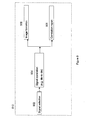
- Figure 9 shows a general image processing flow suitable for some embodiments of this invention. This flow may correspond to step 810 of Figure 8 .
- the baseline diffraction pattern is selected.
- correlation between the current far-field pattern and the baseline information is performed at a step 904. This may include least squares fitting and cross-correlation analysis of the diffraction spots in the diffraction signals.
- the result can provide real time error statistics (output 906) for in-line inspection or generate an image (output 908) for off-line review.
- the baseline information that is selected (step 902) may take several different forms. In one instance, it is information from an adjacent pattern or cell on the same die. This is a cell-to-cell comparison in which similar regions of the same die are illuminated and compared. In another instance, it is information from a die on a semiconductor wafer, similar to the die currently being evaluated. This is a die-to-die comparison in which the same region of multiple dies are illuminated and compared. In yet another instance, it is information from a die on a different semiconductor wafer, similar to the die currently being evaluated. This is a wafer-to-wafer comparison in which the same region of a die on different wafers are illuminated and compared.
- the baseline information can be a stored far-field pattern for a similar surface having known characteristics (e.g., via depth, diameter, and tilt), or it is from a known good surface.
- the stored baseline far-field pattern may have been generated earlier from a sample having such known characteristics.
- the baseline far-field pattern may be generated by a mathematical simulation of the far-field pattern for a surface having specified features.
- Principles underlying effective modeling of diffraction patterns from arbitrary surfaces are described by L. Li in "New formulation of the Fourier modal method for crossed surface-relief gratings" Journal of the Optical Society of America A, vol. 14, No. 10, pp. 2758-67 (1997 ), and in Li, "Modal Method by Fourier expansion for modeling crossed gratings," SPIE proceedings, vol. 3010, pp. 18-29 (1997 ).
- the type of baseline information selected may depend on the information the comparison will provide. For example, in the semiconductor industry problems with a reticle will typically be limited to specific features on one of multiple dies on the reticle. Thus, a die-to-die comparison may be most appropriate for reticle evaluation. In the case of a process problem such as an over aggressive etch, all die may suffer from the same problem (e.g., vias cut too deeply into the substrate). When this occurs, a die-to-die comparison may not be appropriate, as it would only show a discrepancy between the different dies on the same wafer (all die would suffer from the same problem). In this case, the baseline might be a far-field pattern for a die known to have vias of the proper depth, diameter, and tilt. Alternatively, the same section of a wafer or die can be monitored from wafer-to-wafer to get trend data and statistics useful for diagnosing future process excursions.
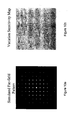
- Figs 10a and 10b An example of this type of computer simulation is shown in Figs 10a and 10b.
- Fig. 10a is a simulation of the expected far-field pattern produced by an array of vias.
- Fig. 10b shows the relative change in each of the orders due to the process error. The more the process variation effects a particular order, the darker or brighter the order will appear compared to the background gray level. Fig 10b shows the orders farther from the specular reflection are more sensitive to the process variation.
- the orders that contain desirable information can be used to improve the computer correlation in one example embodiment. For example, with repeating via arrays, a correlation of the diffraction orders among dies may be performed to identify surface locations with errors. With non-repeating via distributions, Fourier plane zone to zone correlation among dies may be performed.
- modifications to the apparatus that enhance the measurement of the diffraction patterns can be considered. For example, a manufacturer concerned about under etching may want to focus on those regions of the far-field containing the most information about via depth. But it may not know how to identify the spots actually containing that information.
- An accurate mathematical model can provide the identity of such orders for a given apparatus set up and expected via layout. The model could also show how changes in the apparatus set up or via layout will affect the diffraction pattern. Then, the detector orientation, illumination source and angle, and filter configuration (if any) can be chosen to increase the signal-to-noise ratio of those far-field regions containing the information of interest.
- Figure 11 shows a general error classification flow suitable for some embodiments of this invention. This flow may correspond to step 822 of Figure 8 .
- the method of error classification is chosen. Error classification in this invention may be employed in several ways. Some of these are process excursion identification (step 1104), heuristic analysis of specific process errors (step 1106), comparison analysis of specific process errors (step 1108), and search for common defect signatures (step 1110). After error classification is finished, a error classification report can be generated in step 1112.
- One simple approach to classification is to identify when a given die or region of a surface has a diffraction pattern that does not match the expected pattern. This notifies the operator of a potential process excursion without specifying what type of problem it might be (step 1104). Further testing using techniques (e.g., electron microscopy or ion milling) other than those described herein may then be employed to classify the type of error.
- techniques e.g., electron microscopy or ion milling
- a system may classify errors by correlating at least some portion of the far-field pattern with particular errors. For example, an increased intensity in a particular cluster of diffraction orders may indicate there are under etched vias.
- a system suitable for classifying errors according to this technique will contain heuristics for classifying different types of deviations from the baseline information (step 1106).
- An example of this type of classification is shown in the die-to-die comparison in Figs. 12a and 12b.
- Figs. 12a and 12b show a comparison of high angle diffracted orders for a die with known good vias to dies on wafers with unknown via profiles.
- Fig. 12a shows that all the dies on this wafer very closely match the known good die, so this wafer is acceptable.
- Fig. 12b shows the center dies on this wafer do not match the known good die and suffer from under etching.
- a system may classify errors by comparing the far-field pattern of the currently evaluated region against information stored in a baseline database (step 1108).
- the far-field patterns or data about the sensitivity of different far-field regions stored in the baseline database will be associated with various surface conditions. If the current far-field pattern does not accurately match the expected far-field pattern, then the system may compare the current far-field pattern against each of the other relevant far-field patterns in the baseline database. The one that most closely resembles the current far-field pattern effectively classifies the surface error as being that type associated with the matched pattern. The technique may not find an exact match. Nevertheless, it can indicate a likely form and magnitude of the process excursion. On example of such a classification is to compare the process excursion to the previous process history.
- Trends in process data can identify process excursions before they become critical and suggest preventive correction.
- a hypothetical example is shown in Fig 13 .
- a weekly process excursion chart shows that when a filter is due for replacement, an unacceptable process excursion occurs.
- the solution to this problem may be to replace the filter when the data indicates a similar unacceptable process excursion is about to occur.
- the optional memory or baseline database 528 of stored diffraction patterns is coupled to computer 420 as shown in Figure 5 .
- the baseline database may also contain the far-field patterns of surfaces having variations in one or more parameters.
- the database includes the expected far-field patterns for a perfectly formed surface, a surface in which only the opening depth varies from nominal, a surface in which only the opening diameter varies from the nominal, and a surface in which only the opening tilt varies from the nominal.
- the diffraction patterns in the database represent only minor deviations from the nominal surface features.
- the database will also include other far-field patterns to more specifically characterize the deviation from nominal.
- the database may include one far-field pattern for openings having a greater than nominal diameter and another far-field pattern for openings having a less than nominal diameter.
- the deviating far-field patterns will have a certain "signature" of variation in intensity from the nominal case. If a surface under consideration contains the same signature in the specified orders, that surface can be classified as having the variation indicated by the database far-field pattern that it best matches.
Landscapes
- Physics & Mathematics (AREA)
- General Physics & Mathematics (AREA)
- General Health & Medical Sciences (AREA)
- Chemical & Material Sciences (AREA)
- Analytical Chemistry (AREA)
- Biochemistry (AREA)
- Life Sciences & Earth Sciences (AREA)
- Health & Medical Sciences (AREA)
- Immunology (AREA)
- Pathology (AREA)
- Investigating Materials By The Use Of Optical Means Adapted For Particular Applications (AREA)
- Testing Or Measuring Of Semiconductors Or The Like (AREA)
- Length Measuring Devices By Optical Means (AREA)
Abstract
Claims (25)
- Procédé (800) pour analyser l'état d'une surface (14, 16, 604) d'un appareil électronique (408), la surface ayant un motif défini, le procédé comprenant :(a) éclairer (806) une première région de la surface de sorte que de la lumière est diffusée et diffractée sur une pluralité de caractéristiques topologiques répétitives de la surface ;(b) détecter (808) la lumière diffusée et diffractée dans le champ lointain de la première région de la surface produite par l'éclairage de la première région de la surface, la lumière diffusée et diffractée dans le champ lointain étant détectée dans le plan de Fourier ;(c) comparer (810, 902, 904) le motif de régions brillantes et sombres d'interférences constructives et destructives d'un motif de diffraction de champ lointain de la lumière diffusée et diffractée dans le champ lointain, au motif de régions brillantes et sombres d'interférences constructives et destructives d'un motif de diffraction de base d'une lumière diffractée par une région de base ayant un état correspondant à un état attendu de la première région ;(d) déterminer (820) que la première région est inacceptable lorsque l'on détermine (812) que le motif des régions brillantes et sombres du motif diffracté dans le champ lointain de la première région dévie considérablement du motif des régions brillantes et sombres du motif de diffraction de base ;(e) déterminer (814) que la première région est acceptable lorsque l'on détermine (812) que le motif des régions brillantes et sombres du motif diffracté dans le champ lointain de la première région ne dévie pas considérablement du motif des régions brillantes et sombres du motif de diffraction de base, et caractérisé en ce que le procédé comprend en outre :simuler un motif de champ lointain attendu produit par une erreur de traitement particulière ; etidentifier les ordres de diffraction du motif de champ lointain attendu qui sont plus sensibles à l'erreur de traitement particulière, les ordres identifiés étant utilisés pour améliorer la comparaison (c).
- Procédé selon la revendication 1, dans lequel la lumière diffusée et diffractée dans le champ lointain par la première région de la surface forme un motif de diffraction dans le champ lointain dont un seul point de lumière est reproduit en image.
- Procédé selon la revendication 1, dans lequel l'éclairage est réalisé en utilisant une source de lumière cohérente monochromatique (402).
- Procédé selon la revendication 3, dans lequel la source de lumière cohérente monochromatique (402) est un laser.
- Procédé selon la revendication 1, dans lequel la surface (14, 16, 604) est une surface de plaquette semi-conductrice, la première région est une première puce ou zone sur la plaquette semi-conductrice, et la région de base est une seconde puce ou zone sur la plaquette semi-conductrice.
- Procédé selon la revendication 1, dans lequel le motif de diffraction de base est fait de données de diffraction extraites d'une surface ayant l'état attendu de la première région.
- Procédé selon la revendication 1, comprenant en outre les étapes de sélectionner le motif de base à partir d'une base de données de motifs, la base de données de motifs comprenant des motifs de diffraction de régions qui varient par rapport à un motif nominal pour la première région.
- Procédé selon la revendication 1, comprenant en outre :filtrer ou polariser un motif de diffraction dans le champ lointain avant de détecter la lumière diffusée et diffractée dans le champ lointain par la première région de la surface.
- Procédé selon la revendication 1, dans lequel la première région comprend une première partie d'ouvertures (410) dans un film (408) sur ladite surface et le motif de diffraction de base est obtenu à partir d'une seconde partie d'ouvertures (410) dans ledit film (408) sur ladite surface, dans lequel la comparaison est réalisée pour déterminer s'il existe des variations dans ladite première partie d'ouvertures (410) et la seconde partie d'ouvertures (410).
- Procédé selon la revendication 9, dans lequel le film (408) est une couche diélectrique sur une plaquette semi-conductrice.
- Procédé selon la revendication 10, dans lequel les ouvertures (410) sont des trous de contact ou d'interconnexion dans la couche diélectrique.
- Procédé selon la revendication 9, dans lequel la première partie est une première puce sur une plaquette semi-conductrice (408) et dans lequel la seconde partie est une seconde puce sur la plaquette semi-conductrice (408).
- Procédé selon la revendication 9, dans lequel la détection de la lumière diffusée et diffractée dans le champ lointain produite par l'éclairage de la première partie et de la seconde partie comprend l'étape de détecter la lumière diffusée et diffractée dans le champ lointain dans le plan de Fourier.
- Procédé selon la revendication 9, dans lequel la détection de la lumière diffusée et diffractée dans le champ lointain produite par l'éclairage de la première partie et de la seconde partie comprend l'étape de détecter de multiples ordres d'éclairage diffracté.
- Appareil pour évaluer l'état de caractéristiques topologiques sur une surface de substrat, l'appareil comprenant :une source de lumière (402) conçue pour diriger une lumière (404) sur la surface de substrat (408) de sorte que la lumière (412) est diffusée et diffractée par une pluralité de caractéristiques topologiques répétitives (410) sur la surface de substrat ;un détecteur (418) configuré pour capturer et transmettre un motif de diffraction dans le champ lointain d'interférences constructives et destructives de la lumière diffusée et diffractée par la surface de substrat, dans lequel le motif de diffraction dans le champ lointain est détecté dans le plan de Fourier ; etun ordinateur (420) configuré pour (i) comparer le motif de diffraction dans le champ lointain provenant de la surface de substrat avec un motif de diffraction de base d'interférences constructives et destructives de la lumière diffusée et diffractée par une surface de base ayant un état correspondant à un état attendu de la surface de substrat, (ii) lorsque l'on détermine que le motif diffracté dans le champ lointain par la première région dévie considérablement du motif de diffraction de base, déterminer que la première région est inacceptable, et (iii) lorsque l'on détermine que le motif diffracté dans le champ lointain par la première région ne dévie pas considérablement du motif de diffraction de base, déterminer que la première région est acceptable, caractérisé en ce que l'ordinateur est également configuré pour :simuler un motif de champ lointain attendu produit par une erreur de traitement particulière ; etidentifier les ordres de diffraction du motif de champ lointain attendu qui sont plus sensibles à l'erreur de traitement particulière, dans lequel les ordres identifiés sont utilisés pour améliorer la comparaison (i).
- Appareil selon la revendication 15, comprenant en outre des composants optiques (414) alignés pour capturer la lumière diffusée et diffractée par la surface de substrat et pour la diriger sur le détecteur.
- Appareil selon la revendication 15, comprenant en outre :un dispositif de mémoire pour mémoriser le motif de diffraction de base, le appareil de mémoire étant couplé à l'ordinateur (420) ou étant un composant de l'ordinateur.
- Appareil selon la revendication 17, dans lequel l'appareil de mémoire est une base de données (528) mémorisant une pluralité de motifs de diffraction de base pour de multiples états attendus de la surface de substrat.
- Appareil selon la revendication 15, dans lequel la source de lumière (402) est une source de lumière cohérente.
- Appareil selon la revendication 19, dans lequel la source de lumière (402) est un laser.
- Appareil selon la revendication 15, dans lequel le détecteur (418) est une caméra.
- Appareil selon la revendication 15, dans lequel le détecteur (418) est un appareil à couplage de charge ou un réseau de photodiodes.
- Appareil selon la revendication 15, comprenant en outre un filtre de Fourier (526) orienté pour bloquer une ou plusieurs régions du motif de diffraction dans le champ lointain provenant de la surface de substrat.
- Appareil selon la revendication 15, comprenant également des composants optiques comprenant un microscope pour fournir des vues de la surface de substrat.
- Appareil selon la revendication 15, le appareil étant configuré pour ne détecter qu'une partie de la lumière diffusée et diffractée, laquelle partie est sensible à un état de surface particulier.
Applications Claiming Priority (3)
| Application Number | Priority Date | Filing Date | Title |
|---|---|---|---|
| US09/107,391 US6137570A (en) | 1998-06-30 | 1998-06-30 | System and method for analyzing topological features on a surface |
| US107391 | 1998-06-30 | ||
| PCT/US1999/013150 WO2000000817A1 (fr) | 1998-06-30 | 1999-06-10 | Systeme et procede d'analyse des caracteristiques topologiques d'une surface |
Publications (3)
| Publication Number | Publication Date |
|---|---|
| EP1092145A1 EP1092145A1 (fr) | 2001-04-18 |
| EP1092145A4 EP1092145A4 (fr) | 2002-10-02 |
| EP1092145B1 true EP1092145B1 (fr) | 2009-01-14 |
Family
ID=22316409
Family Applications (1)
| Application Number | Title | Priority Date | Filing Date |
|---|---|---|---|
| EP99930207A Expired - Lifetime EP1092145B1 (fr) | 1998-06-30 | 1999-06-10 | Systeme et procede d'analyse des caracteristiques topologiques d'une surface |
Country Status (6)
| Country | Link |
|---|---|
| US (1) | US6137570A (fr) |
| EP (1) | EP1092145B1 (fr) |
| JP (1) | JP3922885B2 (fr) |
| AU (1) | AU4679199A (fr) |
| DE (1) | DE69940315D1 (fr) |
| WO (1) | WO2000000817A1 (fr) |
Cited By (1)
| Publication number | Priority date | Publication date | Assignee | Title |
|---|---|---|---|---|
| DE102012022966A1 (de) * | 2012-11-21 | 2014-05-22 | Friedrich-Schiller-Universität Jena | Verfahren zur Auswertung von durch schmalbandige, kurzwellige, kohärente Laserstrahlung erzeugten Streubildern von Objektiven, insbesondere zur Verwendung in der XUV-Mikroskopie |
Families Citing this family (92)
| Publication number | Priority date | Publication date | Assignee | Title |
|---|---|---|---|---|
| US6612676B1 (en) | 1998-11-17 | 2003-09-02 | Pitney Bowes Inc. | Apparatus and method for real-time measurement of digital print quality |
| US6350006B1 (en) * | 1998-11-17 | 2002-02-26 | Pitney Bowes Inc. | Optical ink drop detection apparatus and method for monitoring operation of an ink jet printhead |
| WO2000035002A1 (fr) * | 1998-12-04 | 2000-06-15 | Semiconductor 300 Gmbh & Co. Kg | Dispositif et procede de controle optique de processus de fabrication de surfaces microstructurees dans la production de semi-conducteurs |
| WO2000054325A1 (fr) * | 1999-03-10 | 2000-09-14 | Nova Measuring Instruments Ltd. | Procede et appareil pour le controle d'un procede de planarisation chimico-mecanique applique a des objets a motif a base de metal |
| US6369888B1 (en) * | 1999-11-17 | 2002-04-09 | Applied Materials, Inc. | Method and apparatus for article inspection including speckle reduction |
| US6429943B1 (en) * | 2000-03-29 | 2002-08-06 | Therma-Wave, Inc. | Critical dimension analysis with simultaneous multiple angle of incidence measurements |
| US7136159B2 (en) * | 2000-09-12 | 2006-11-14 | Kla-Tencor Technologies Corporation | Excimer laser inspection system |
| JP3266602B1 (ja) * | 2000-10-30 | 2002-03-18 | 洋一 奥寺 | アドレス照会システム、コンピュータプログラム製品及びその方法 |
| US6433878B1 (en) | 2001-01-29 | 2002-08-13 | Timbre Technology, Inc. | Method and apparatus for the determination of mask rules using scatterometry |
| US6898037B2 (en) | 2001-02-20 | 2005-05-24 | Seagate Technology Llc | Optical equipment assemblies and techniques |
| US7515279B2 (en) | 2001-03-02 | 2009-04-07 | Nanometrics Incorporated | Line profile asymmetry measurement |
| KR100536646B1 (ko) * | 2001-03-02 | 2005-12-14 | 액센트 옵티칼 테크놀로지스 인코포레이티드 | 산란 측정법을 이용한 라인 프로파일 비대칭 측정 |
| US6675118B2 (en) * | 2001-03-19 | 2004-01-06 | Hewlett-Packard Development Company, L.P. | System and method of determining the noise sensitivity characterization for an unknown circuit |
| US6597446B2 (en) * | 2001-03-22 | 2003-07-22 | Sentec Corporation | Holographic scatterometer for detection and analysis of wafer surface deposits |
| US20020177245A1 (en) * | 2001-03-29 | 2002-11-28 | Sonderman Thomas J. | Method and apparatus for controlling feature critical dimensions based on scatterometry derived profile |
| US6603541B2 (en) | 2001-06-28 | 2003-08-05 | Kla-Tencor Technologies Corporation | Wafer inspection using optimized geometry |
| US6804005B2 (en) * | 2002-05-02 | 2004-10-12 | Timbre Technologies, Inc. | Overlay measurements using zero-order cross polarization measurements |
| US6862491B2 (en) * | 2002-05-22 | 2005-03-01 | Applied Materials Israel, Ltd. | System and method for process variation monitor |
| US7155052B2 (en) * | 2002-06-10 | 2006-12-26 | Tokyo Seimitsu (Israel) Ltd | Method for pattern inspection |
| US6775015B2 (en) * | 2002-06-18 | 2004-08-10 | Timbre Technologies, Inc. | Optical metrology of single features |
| US20050122509A1 (en) * | 2002-07-18 | 2005-06-09 | Leica Microsystems Semiconductor Gmbh | Apparatus for wafer inspection |
| EP1576355A2 (fr) * | 2002-09-30 | 2005-09-21 | Applied Materials Israel Ltd. | Systeme d'eclairage pour inspection optique |
| US7123356B1 (en) | 2002-10-15 | 2006-10-17 | Kla-Tencor Technologies Corp. | Methods and systems for inspecting reticles using aerial imaging and die-to-database detection |
| US7027143B1 (en) | 2002-10-15 | 2006-04-11 | Kla-Tencor Technologies Corp. | Methods and systems for inspecting reticles using aerial imaging at off-stepper wavelengths |
| US7379175B1 (en) | 2002-10-15 | 2008-05-27 | Kla-Tencor Technologies Corp. | Methods and systems for reticle inspection and defect review using aerial imaging |
| US7133119B1 (en) | 2002-12-17 | 2006-11-07 | Kla-Tencor Technologies Corp. | Systems for simulating high NA and polarization effects in aerial images |
| US7180658B2 (en) * | 2003-02-21 | 2007-02-20 | Kla-Tencor Technologies Corporation | High performance catadioptric imaging system |
| US20040181768A1 (en) * | 2003-03-12 | 2004-09-16 | Krukar Richard H. | Model pattern simulation of semiconductor wafer processing steps |
| US7041998B2 (en) * | 2003-03-24 | 2006-05-09 | Photon Dynamics, Inc. | Method and apparatus for high-throughput inspection of large flat patterned media using dynamically programmable optical spatial filtering |
| US7327457B2 (en) * | 2003-12-19 | 2008-02-05 | N&K Technology, Inc. | Apparatus and method for optical characterization of a sample over a broadband of wavelengths while minimizing polarization changes |
| US7248364B2 (en) * | 2003-12-19 | 2007-07-24 | N&K Technology, Inc. | Apparatus and method for optical characterization of a sample over a broadband of wavelengths with a small spot size |
| US7050880B2 (en) * | 2003-12-30 | 2006-05-23 | Sc Solutions | Chemical-mechanical planarization controller |
| JP4758358B2 (ja) | 2004-01-29 | 2011-08-24 | ケーエルエー−テンカー コーポレイション | レチクル設計データにおける欠陥を検出するためのコンピュータに実装される方法 |
| USH2180H1 (en) * | 2004-03-23 | 2007-02-06 | Michael R. Brininstool | Coiled optical Bragg radiating aperture system |
| JP4904034B2 (ja) | 2004-09-14 | 2012-03-28 | ケーエルエー−テンカー コーポレイション | レチクル・レイアウト・データを評価するための方法、システム及び搬送媒体 |
| JP4645113B2 (ja) * | 2004-09-21 | 2011-03-09 | 日本電気株式会社 | 光検査方法及び光検査装置並びに光検査システム |
| US7274465B2 (en) * | 2005-02-17 | 2007-09-25 | Timbre Technologies, Inc. | Optical metrology of a structure formed on a semiconductor wafer using optical pulses |
| US20060285110A1 (en) * | 2005-02-25 | 2006-12-21 | Accent Optical Technologies, Inc. | Apparatus and method for enhanced critical dimension scatterometry |
| US7769225B2 (en) | 2005-08-02 | 2010-08-03 | Kla-Tencor Technologies Corp. | Methods and systems for detecting defects in a reticle design pattern |
| US8111374B2 (en) * | 2005-09-09 | 2012-02-07 | Nikon Corporation | Analysis method, exposure method, and device manufacturing method |
| US8041103B2 (en) | 2005-11-18 | 2011-10-18 | Kla-Tencor Technologies Corp. | Methods and systems for determining a position of inspection data in design data space |
| US7676077B2 (en) | 2005-11-18 | 2010-03-09 | Kla-Tencor Technologies Corp. | Methods and systems for utilizing design data in combination with inspection data |
| US7570796B2 (en) | 2005-11-18 | 2009-08-04 | Kla-Tencor Technologies Corp. | Methods and systems for utilizing design data in combination with inspection data |
| US7440094B2 (en) * | 2005-11-30 | 2008-10-21 | Wafermasters Incorporated | Optical sample characterization system |
| JP4760564B2 (ja) | 2006-06-20 | 2011-08-31 | 日本電気株式会社 | パターン形状の欠陥検出方法及び検出装置 |
| US7643147B2 (en) * | 2006-11-03 | 2010-01-05 | Neuropace, Inc. | Method and system for device identification |
| WO2008077100A2 (fr) | 2006-12-19 | 2008-06-26 | Kla-Tencor Corporation | Systèmes et procédés de création de procédures de contrôle |
| WO2008086282A2 (fr) | 2007-01-05 | 2008-07-17 | Kla-Tencor Corporation | Procédés et systèmes pour utiliser des informations électriques dans le cadre de la fabrication d'un dispositif sur une tranche afin d'accomplir une ou plusieurs fonctions liées à des défauts |
| US7738093B2 (en) | 2007-05-07 | 2010-06-15 | Kla-Tencor Corp. | Methods for detecting and classifying defects on a reticle |
| US7962863B2 (en) | 2007-05-07 | 2011-06-14 | Kla-Tencor Corp. | Computer-implemented methods, systems, and computer-readable media for determining a model for predicting printability of reticle features on a wafer |
| US8213704B2 (en) | 2007-05-09 | 2012-07-03 | Kla-Tencor Corp. | Methods and systems for detecting defects in a reticle design pattern |
| SG149763A1 (en) * | 2007-07-12 | 2009-02-27 | Applied Materials Israel Ltd | Method and system for evaluating an object that has a repetitive pattern |
| US7796804B2 (en) | 2007-07-20 | 2010-09-14 | Kla-Tencor Corp. | Methods for generating a standard reference die for use in a die to standard reference die inspection and methods for inspecting a wafer |
| US7711514B2 (en) | 2007-08-10 | 2010-05-04 | Kla-Tencor Technologies Corp. | Computer-implemented methods, carrier media, and systems for generating a metrology sampling plan |
| JP5425779B2 (ja) | 2007-08-20 | 2014-02-26 | ケーエルエー−テンカー・コーポレーション | 実際の欠陥が潜在的にシステム的な欠陥であるか、または潜在的にランダムな欠陥であるかを判断する、コンピューターに実装された方法 |
| IL188029A0 (en) * | 2007-12-10 | 2008-11-03 | Nova Measuring Instr Ltd | Optical method and system |
| NL1036279A1 (nl) * | 2007-12-13 | 2009-06-16 | Asml Netherlands Bv | A device for transmission image detection for use in a lithographic projection apparatus and a method for determining third order distortions of a patterning device and/or a projection system of such a lithographic apparatus. |
| US20090230199A1 (en) * | 2008-03-12 | 2009-09-17 | Lasercard Corporation | Diffractive data storage |
| US8139844B2 (en) | 2008-04-14 | 2012-03-20 | Kla-Tencor Corp. | Methods and systems for determining a defect criticality index for defects on wafers |
| US7649624B1 (en) * | 2008-07-16 | 2010-01-19 | Crystal Technology, Inc. | Systems and methods for detecting scratches on non-semiconductor wafer surfaces |
| KR101841897B1 (ko) | 2008-07-28 | 2018-03-23 | 케이엘에이-텐코어 코오포레이션 | 웨이퍼 상의 메모리 디바이스 영역에서 검출된 결함들을 분류하기 위한 컴퓨터-구현 방법들, 컴퓨터-판독 가능 매체, 및 시스템들 |
| US9625937B2 (en) * | 2008-08-18 | 2017-04-18 | Kla-Tencor Corporation | Computation efficiency by diffraction order truncation |
| US8775101B2 (en) | 2009-02-13 | 2014-07-08 | Kla-Tencor Corp. | Detecting defects on a wafer |
| TW201100787A (en) * | 2009-02-18 | 2011-01-01 | Nikon Corp | Surface examining device and surface examining method |
| US8204297B1 (en) | 2009-02-27 | 2012-06-19 | Kla-Tencor Corp. | Methods and systems for classifying defects detected on a reticle |
| US8112241B2 (en) | 2009-03-13 | 2012-02-07 | Kla-Tencor Corp. | Methods and systems for generating an inspection process for a wafer |
| KR101452852B1 (ko) * | 2009-10-13 | 2014-10-22 | 에이에스엠엘 네델란즈 비.브이. | 검사 방법 및 장치 |
| JP5216752B2 (ja) | 2009-11-18 | 2013-06-19 | 株式会社日立ハイテクノロジーズ | 欠陥検出方法及び欠陥検出装置並びにこれを備えた欠陥観察装置 |
| US8781781B2 (en) | 2010-07-30 | 2014-07-15 | Kla-Tencor Corp. | Dynamic care areas |
| JP5593209B2 (ja) * | 2010-11-30 | 2014-09-17 | 株式会社日立ハイテクノロジーズ | 検査装置 |
| WO2012115013A1 (fr) * | 2011-02-25 | 2012-08-30 | 株式会社ニコン | Appareil d'inspection et procédé de fabrication d'un dispositif semi-conducteur |
| US9170211B2 (en) | 2011-03-25 | 2015-10-27 | Kla-Tencor Corp. | Design-based inspection using repeating structures |
| US9087367B2 (en) | 2011-09-13 | 2015-07-21 | Kla-Tencor Corp. | Determining design coordinates for wafer defects |
| JP5288297B2 (ja) * | 2011-12-27 | 2013-09-11 | 新日鐵住金株式会社 | ねじ付き管の端部形状測定方法 |
| US8831334B2 (en) | 2012-01-20 | 2014-09-09 | Kla-Tencor Corp. | Segmentation for wafer inspection |
| US8826200B2 (en) | 2012-05-25 | 2014-09-02 | Kla-Tencor Corp. | Alteration for wafer inspection |
| US9189844B2 (en) | 2012-10-15 | 2015-11-17 | Kla-Tencor Corp. | Detecting defects on a wafer using defect-specific information |
| US10088345B1 (en) * | 2012-12-04 | 2018-10-02 | Kla-Tencor Corporation | Haze and defect distribution and aperture configuration in surface metrology inspectors |
| TWI470210B (zh) * | 2012-12-17 | 2015-01-21 | Taiwan Power Testing Technology Co Ltd | 顯示裝置之光學層件之缺陷檢測方法 |
| US9053527B2 (en) | 2013-01-02 | 2015-06-09 | Kla-Tencor Corp. | Detecting defects on a wafer |
| US9134254B2 (en) | 2013-01-07 | 2015-09-15 | Kla-Tencor Corp. | Determining a position of inspection system output in design data space |
| US9311698B2 (en) | 2013-01-09 | 2016-04-12 | Kla-Tencor Corp. | Detecting defects on a wafer using template image matching |
| KR102019534B1 (ko) | 2013-02-01 | 2019-09-09 | 케이엘에이 코포레이션 | 결함 특유의, 다중 채널 정보를 이용한 웨이퍼 상의 결함 검출 |
| US9865512B2 (en) | 2013-04-08 | 2018-01-09 | Kla-Tencor Corp. | Dynamic design attributes for wafer inspection |
| US9310320B2 (en) | 2013-04-15 | 2016-04-12 | Kla-Tencor Corp. | Based sampling and binning for yield critical defects |
| US10094774B2 (en) | 2015-08-12 | 2018-10-09 | Industrial Technology Research Institute | Scattering measurement system and method |
| EP3379234B1 (fr) * | 2015-11-17 | 2025-08-27 | Korea Advanced Institute of Science and Technology | Appareil permettant de détecter des propriétés d'échantillon à l'aide d'un capteur d'ondes chaotiques |
| EP3208657A1 (fr) * | 2016-02-22 | 2017-08-23 | Paul Scherrer Institut | Procédé et système d'inspection de défaut à haut rendement utilisant le contraste dans le domaine de fréquence spatiale réduite |
| EP3467483B1 (fr) * | 2016-06-02 | 2023-09-20 | The Wave Talk, Inc. | Dispositif d'inspection de structure de motif et procédé d'inspection |
| KR101971272B1 (ko) * | 2016-06-02 | 2019-08-27 | 주식회사 더웨이브톡 | 패턴 구조물 검사 장치 및 검사 방법 |
| DE102017205212A1 (de) * | 2017-03-28 | 2018-10-04 | Carl Zeiss Smt Gmbh | Verfahren zum Detektieren von Partikeln an der Oberfläche eines Objekts, Wafer und Maskenblank |
| US12222659B2 (en) | 2023-01-18 | 2025-02-11 | Applied Materials, Inc. | Metrology system for packaging applications |
Family Cites Families (33)
| Publication number | Priority date | Publication date | Assignee | Title |
|---|---|---|---|---|
| US4347001A (en) * | 1978-04-03 | 1982-08-31 | Kla Instruments Corporation | Automatic photomask inspection system and apparatus |
| US4247203A (en) * | 1978-04-03 | 1981-01-27 | Kla Instrument Corporation | Automatic photomask inspection system and apparatus |
| JPS60708B2 (ja) * | 1979-11-07 | 1985-01-09 | 株式会社東芝 | 欠陥検査装置 |
| US4448532A (en) * | 1981-03-31 | 1984-05-15 | Kla Instruments Corporation | Automatic photomask inspection method and system |
| US4926489A (en) * | 1983-03-11 | 1990-05-15 | Kla Instruments Corporation | Reticle inspection system |
| US4579455A (en) * | 1983-05-09 | 1986-04-01 | Kla Instruments Corporation | Photomask inspection apparatus and method with improved defect detection |
| US4595289A (en) * | 1984-01-25 | 1986-06-17 | At&T Bell Laboratories | Inspection system utilizing dark-field illumination |
| JPH07118440B2 (ja) * | 1986-07-09 | 1995-12-18 | 東芝機械株式会社 | 電子ビ−ム描画装置 |
| CA1242815A (fr) * | 1987-03-20 | 1988-10-04 | Pak K. Leung | Methode de detection de defauts dans les configurations de plaquettes de semiconducteur |
| US4806774A (en) * | 1987-06-08 | 1989-02-21 | Insystems, Inc. | Inspection system for array of microcircuit dies having redundant circuit patterns |
| US5131755A (en) * | 1988-02-19 | 1992-07-21 | Chadwick Curt H | Automatic high speed optical inspection system |
| JP2796316B2 (ja) * | 1988-10-24 | 1998-09-10 | 株式会社日立製作所 | 欠陥または異物の検査方法およびその装置 |
| US5241369A (en) * | 1990-10-01 | 1993-08-31 | Mcneil John R | Two-dimensional optical scatterometer apparatus and process |
| IL125217A (en) * | 1990-12-04 | 1999-10-28 | Orbot Instr Ltd | Apparatus and method for microscopic inspection of articles |
| US5177559A (en) * | 1991-05-17 | 1993-01-05 | International Business Machines Corporation | Dark field imaging defect inspection system for repetitive pattern integrated circuits |
| JP3148353B2 (ja) * | 1991-05-30 | 2001-03-19 | ケーエルエー・インストルメンツ・コーポレーション | 電子ビーム検査方法とそのシステム |
| US5410400A (en) * | 1991-06-26 | 1995-04-25 | Hitachi, Ltd. | Foreign particle inspection apparatus |
| US5539514A (en) * | 1991-06-26 | 1996-07-23 | Hitachi, Ltd. | Foreign particle inspection apparatus and method with front and back illumination |
| JP3323537B2 (ja) * | 1991-07-09 | 2002-09-09 | キヤノン株式会社 | 微細構造評価装置及び微細構造評価法 |
| US5563702A (en) * | 1991-08-22 | 1996-10-08 | Kla Instruments Corporation | Automated photomask inspection apparatus and method |
| DE69208413T2 (de) * | 1991-08-22 | 1996-11-14 | Kla Instr Corp | Gerät zur automatischen Prüfung von Photomaske |
| US5185636A (en) * | 1991-12-31 | 1993-02-09 | Corning Incorporated | Method for detecting defects in fibers |
| US5502311A (en) * | 1992-01-17 | 1996-03-26 | Nikon Corporation | Method of and apparatus for detecting plane position |
| US5276498A (en) * | 1992-05-12 | 1994-01-04 | Tencor Instruments | Adaptive spatial filter for surface inspection |
| JP3730263B2 (ja) * | 1992-05-27 | 2005-12-21 | ケーエルエー・インストルメンツ・コーポレーション | 荷電粒子ビームを用いた自動基板検査の装置及び方法 |
| JPH06109647A (ja) * | 1992-09-24 | 1994-04-22 | Nikon Corp | 欠陥検査装置 |
| US5513275A (en) * | 1993-01-12 | 1996-04-30 | Board Of Trustees Of The Leland Stanford Junior University | Automated direct patterned wafer inspection |
| US5428442A (en) * | 1993-09-30 | 1995-06-27 | Optical Specialties, Inc. | Inspection system with in-lens, off-axis illuminator |
| JP2695600B2 (ja) * | 1993-10-01 | 1997-12-24 | 浜松ホトニクス株式会社 | 光学検査装置 |
| US5530550A (en) * | 1994-12-21 | 1996-06-25 | Tencor Instruments | Optical wafer positioning system |
| US5506676A (en) * | 1994-10-25 | 1996-04-09 | Pixel Systems, Inc. | Defect detection using fourier optics and a spatial separator for simultaneous optical computing of separated fourier transform components |
| US5659390A (en) * | 1995-02-09 | 1997-08-19 | Inspex, Inc. | Method and apparatus for detecting particles on a surface of a semiconductor wafer having repetitive patterns |
| US5825043A (en) * | 1996-10-07 | 1998-10-20 | Nikon Precision Inc. | Focusing and tilting adjustment system for lithography aligner, manufacturing apparatus or inspection apparatus |
-
1998
- 1998-06-30 US US09/107,391 patent/US6137570A/en not_active Expired - Lifetime
-
1999
- 1999-06-10 EP EP99930207A patent/EP1092145B1/fr not_active Expired - Lifetime
- 1999-06-10 DE DE69940315T patent/DE69940315D1/de not_active Expired - Lifetime
- 1999-06-10 WO PCT/US1999/013150 patent/WO2000000817A1/fr not_active Ceased
- 1999-06-10 JP JP2000557139A patent/JP3922885B2/ja not_active Expired - Fee Related
- 1999-06-10 AU AU46791/99A patent/AU4679199A/en not_active Abandoned
Cited By (1)
| Publication number | Priority date | Publication date | Assignee | Title |
|---|---|---|---|---|
| DE102012022966A1 (de) * | 2012-11-21 | 2014-05-22 | Friedrich-Schiller-Universität Jena | Verfahren zur Auswertung von durch schmalbandige, kurzwellige, kohärente Laserstrahlung erzeugten Streubildern von Objektiven, insbesondere zur Verwendung in der XUV-Mikroskopie |
Also Published As
| Publication number | Publication date |
|---|---|
| US6137570A (en) | 2000-10-24 |
| AU4679199A (en) | 2000-01-17 |
| JP3922885B2 (ja) | 2007-05-30 |
| JP2002519667A (ja) | 2002-07-02 |
| DE69940315D1 (de) | 2009-03-05 |
| WO2000000817A1 (fr) | 2000-01-06 |
| EP1092145A4 (fr) | 2002-10-02 |
| EP1092145A1 (fr) | 2001-04-18 |
Similar Documents
| Publication | Publication Date | Title |
|---|---|---|
| US6137570A (en) | System and method for analyzing topological features on a surface | |
| US5555474A (en) | Automatic rejection of diffraction effects in thin film metrology | |
| US6842259B2 (en) | Analysis of isolated and aperiodic structures with simultaneous multiple angle of incidence measurements | |
| US6429943B1 (en) | Critical dimension analysis with simultaneous multiple angle of incidence measurements | |
| US7046376B2 (en) | Overlay targets with isolated, critical-dimension features and apparatus to measure overlay | |
| US7953567B2 (en) | Defect inspection apparatus and defect inspection method | |
| US8982358B2 (en) | Apparatus and method of measuring roughness and other parameters of a structure | |
| KR101506894B1 (ko) | 웨이퍼의 두 개 또는 그 초과의 특성들을 결정하기 위한 시스템들 및 방법들 | |
| US7505619B2 (en) | System and method for conducting adaptive fourier filtering to detect defects in dense logic areas of an inspection surface | |
| US20140376006A1 (en) | Optical system and method for measurement of one or more parameters of via-holes | |
| JP2007041600A (ja) | レティクル設計パターン内の欠陥を検出するための方法および装置 | |
| WO2007137261A2 (fr) | Procédés et des systèmes servant : à détecter des trous d'aiguille dans un film formé sur une tranche de semi-conducteur, et à suivre la marche d'un outil de traitement thermique. | |
| US7483133B2 (en) | Multiple angle of incidence spectroscopic scatterometer system | |
| US7436505B2 (en) | Computer-implemented methods and systems for determining a configuration for a light scattering inspection system | |
| TWI490963B (zh) | 檢查及處理半導體晶圓之方法 | |
| EP1241465A1 (fr) | Procédé et dispositif de classification de défauts, en particulier sur ou près d'une surface d'un substrat lisse | |
| US20080144034A1 (en) | Systems and methods for blocking specular reflection and suppressing modulation from periodic features on a specimen | |
| KR100684102B1 (ko) | 결함 검사 방법 및 이를 이용한 결함 검사 장치 | |
| JP3476742B2 (ja) | 基板の表面に発生する粒子の材料を識別する方法と装置 | |
| WO2005001577A1 (fr) | Systeme et procede de metrologie optique de plaquettes semi-conductrices |
Legal Events
| Date | Code | Title | Description |
|---|---|---|---|
| PUAI | Public reference made under article 153(3) epc to a published international application that has entered the european phase |
Free format text: ORIGINAL CODE: 0009012 |
|
| 17P | Request for examination filed |
Effective date: 20001212 |
|
| AK | Designated contracting states |
Kind code of ref document: A1 Designated state(s): DE FR GB |
|
| A4 | Supplementary search report drawn up and despatched |
Effective date: 20020816 |
|
| AK | Designated contracting states |
Kind code of ref document: A4 Designated state(s): DE FR GB |
|
| RIC1 | Information provided on ipc code assigned before grant |
Free format text: 7G 01N 21/00 A, 7G 01N 21/956 B |
|
| 17Q | First examination report despatched |
Effective date: 20040414 |
|
| GRAP | Despatch of communication of intention to grant a patent |
Free format text: ORIGINAL CODE: EPIDOSNIGR1 |
|
| RIC1 | Information provided on ipc code assigned before grant |
Ipc: G01N 21/956 20060101AFI20080624BHEP |
|
| GRAS | Grant fee paid |
Free format text: ORIGINAL CODE: EPIDOSNIGR3 |
|
| GRAA | (expected) grant |
Free format text: ORIGINAL CODE: 0009210 |
|
| AK | Designated contracting states |
Kind code of ref document: B1 Designated state(s): DE FR GB |
|
| REG | Reference to a national code |
Ref country code: GB Ref legal event code: FG4D |
|
| REF | Corresponds to: |
Ref document number: 69940315 Country of ref document: DE Date of ref document: 20090305 Kind code of ref document: P |
|
| PLBE | No opposition filed within time limit |
Free format text: ORIGINAL CODE: 0009261 |
|
| STAA | Information on the status of an ep patent application or granted ep patent |
Free format text: STATUS: NO OPPOSITION FILED WITHIN TIME LIMIT |
|
| 26N | No opposition filed |
Effective date: 20091015 |
|
| PGFP | Annual fee paid to national office [announced via postgrant information from national office to epo] |
Ref country code: GB Payment date: 20140627 Year of fee payment: 16 |
|
| PGFP | Annual fee paid to national office [announced via postgrant information from national office to epo] |
Ref country code: FR Payment date: 20140617 Year of fee payment: 16 |
|
| GBPC | Gb: european patent ceased through non-payment of renewal fee |
Effective date: 20150610 |
|
| REG | Reference to a national code |
Ref country code: FR Ref legal event code: ST Effective date: 20160229 |
|
| PG25 | Lapsed in a contracting state [announced via postgrant information from national office to epo] |
Ref country code: GB Free format text: LAPSE BECAUSE OF NON-PAYMENT OF DUE FEES Effective date: 20150610 |
|
| PG25 | Lapsed in a contracting state [announced via postgrant information from national office to epo] |
Ref country code: FR Free format text: LAPSE BECAUSE OF NON-PAYMENT OF DUE FEES Effective date: 20150630 |
|
| PGFP | Annual fee paid to national office [announced via postgrant information from national office to epo] |
Ref country code: DE Payment date: 20160628 Year of fee payment: 18 |
|
| REG | Reference to a national code |
Ref country code: DE Ref legal event code: R119 Ref document number: 69940315 Country of ref document: DE |
|
| PG25 | Lapsed in a contracting state [announced via postgrant information from national office to epo] |
Ref country code: DE Free format text: LAPSE BECAUSE OF NON-PAYMENT OF DUE FEES Effective date: 20180103 |
|
| P01 | Opt-out of the competence of the unified patent court (upc) registered |
Effective date: 20230525 |